Brocade-48000板卡迁移FC4-32
Brocade 48000安装与配置

Brocade 48000安装与配置(一)1 时间和所需物品2 站点准备和Brocade 48000拆箱正确安装和操作的步骤如下:1)提供一个有14U高,73.7厘米(29英寸)深和48.3厘米(19英寸)宽的机架空间。
1U等于4.45厘米(1.75英寸)。
2)计划安装的导向器的背面朝向进风口通道。
为了维护保养方便和冷却需求得到满足,导向器可以被安装朝向任一方向,3)安装设备(“管理线缆” )前,要做好线缆管理的计划。
线缆可以用各种方式被管理,如放置线缆在设备下面,通过线缆槽,或通过使用配线板,然后到设备的任一侧。
4)确保两个专用的分支电路具有如下特点:• 200-240伏交流电压,50 - 60赫兹•符合当地电气法规的带保护的断路开关•供应电路,保险丝,和线径足够与设备名牌上的电气等级匹配•位置接近设备和方便接入•接地插座的安装要求有认证的电工,兼容的电源线注意为了最大限度地提高容错能力,连接的每个电源线要求来自于独立的电源。
5)确保进风口和排风口有一个最小2英寸的空间。
6)确保在运行期间进风口一侧的空气温度是低于40摄氏度(104华氏度)。
警告移动设备时,要使用安全的提升操作注意一个全配的导向器(8 个FC4 - 48端口片,384个端口)重约96公斤(216磅),需要液压千斤顶或协助提升去安装。
7)拆箱和安装导向器。
3 Brocade 48000导向器上架请参考Brocade 手册《14U Rack Mount Kit Installation Procedure》。
该部分没有客户化的内容。
4 Brocade 48000导向器包括的物品导向器标准的装备清单如下:导向器设备包括有:•控制处理插板(CP4)•端口插板和应用插板(根据客户规格指定)•插板槽填充面板 (用于没有被端口片或CP片填充的槽位)• WWN card• WWN bezel•电源•电源填充面板(少于4个电源模块时提供)•风扇组件•线缆管理托盘•机箱门配件套件包含下列项目:• Brocade 48000快速入门指南• Brocade 文档CD•接地静电带•适合该国安装标准的电源线•电源线护圈• RS-232串口线带有安装说明的14U机架安装套件(包括后部支架和底部支持导轨)从Brocade订购可选的(SFP and XFP)。
IGLOO2 FPGA 设备家族之间的设计迁移指南说明书

Application Note AC416February 20141© 2014 Microsemi CorporationMigrating Designs Between IGLOO2 M2GL025 and M2GL050 in VF400 PackageTable of ContentsIntroductionThis document describes how to migrate designs within the IGLOO ®2 field programmable gate array (FPGA) device family between the M2GL025 and M2GL050 devices within the VF400 package. It addresses restrictions and specifications that need to be considered while moving a design between the M2GL025 and M2GL050 devices. This includes pin compatibility between the devices, design and device resources evaluation, I/O banks, standards, and so on. This document also describes the software flow behavior during the migration.Design MigrationIGLOO2 family devices are architecturally compatible with each other. However, attention must be paid to some key areas while migrating a design from one device to another. The following specific points are discussed in this document:•Design and Device Evaluation •I/O Banks and Standards •Pin Migration and Compatibility•Power Supply and Board-Level Considerations •Software FlowDesign and Device EvaluationOne of the initial and main tasks while migrating a design should be to compare the available resources between the two devices. The device resources can be grouped into three different categories:•High Performance Memory Subsystem •Fabric Resources •On-Chip OscillatorsIn addition, necessary design timing analysis and simulations should be performed while migrating designs from one device to another.Each of the following sections focuses on the different aspects of the design and device evaluation categories.Introduction . . . . . . . . . . . . . . . . . . . . . . . . . . . . . . . . . . . . . . . . . . . . . . . . 1Design Migration . . . . . . . . . . . . . . . . . . . . . . . . . . . . . . . . . . . . . . . . . . . . . 1Design and Device Evaluation . . . . . . . . . . . . . . . . . . . . . . . . . . . . . . . . . . . . . . . . . . . . . . . . . . . . . . . . . . . 1I/O Banks and Standards . . . . . . . . . . . . . . . . . . . . . . . . . . . . . . . . . . . . . . . . . . . . . . . . . . . . . . . . . . . . . . . 3Pin Migration and Compatibility . . . . . . . . . . . . . . . . . . . . . . . . . . . . . . . . . . . . . . . . . . . . . . . . . . . . . . . . . . 5Power Supply and Board-Level Considerations . . . . . . . . . . . . . . . . . . . . . . . . . . . . . . . . . . . . . . . . . . . . . . 9Software Flow . . . . . . . . . . . . . . . . . . . . . . . . . . . . . . . . . . . . . . . . . . . . . . . . . . . . . . . . . . . . . . . . . . . . . . 10Conclusion . . . . . . . . . . . . . . . . . . . . . . . . . . . . . . . . . . . . . . . . . . . . . . . 13List of Changes . . . . . . . . . . . . . . . . . . . . . . . . . . . . . . . . . . . . . . . . . . . . . 13Migrating Designs Between IGLOO2 M2GL025 and M2GL050 in VF400 Package2High Performance Memory SubsystemTable1 provides a high-level summary of the differences between the M2GL025 and M2GL050 high performance memory subsystem (HPMS) blocks. Based on the different HPMS resources and features, migration from one device to another can be planned to avoid any resource conflicts or issues. Fabric ResourcesTable2 gives a high-level summary of the differences between M2GL025 and M2GL050 fabric resources. Based on the differences, effective logic count, RAM size, and number of I/Os, migration can be evaluated and planned from one device to another without any resource conflicts or issues.On-Chip OscillatorsTable3 shows the summary of IGLOO2 on-chip oscillators that are the primary sources for generating free-running clocks.Table 1 • HPMS Features Per Package or DeviceFeatureVF400 PackageM2GL025 and M2GL025T M2GL050 and M2GL050T Fabric interfaces (FIC) 1 (FIC_0) 2 (FIC_0 and FIC_1) Memory subsytem DDR (MDDR)1X181X182eNVM (Kbytes) 256256eSRAM (Kbytes)6464eSRAM (non-SECDED) (Kbytes)8080SPI, HPDMA, PDMA22SDRAM through SMC_FIC Yes YesNotes:1.DDR supports x18, x16, x9, and x8 modes2.DDR supports x18 and x16 modesTable 2 • Summary of the Fabric Features Supported Per DeviceFabric Features (Logic, DSP, and Memory)VF400 PackageM2GL025 andM2GL025TM2GL050 andM2GL050T Logic/DSP Logic Modules (4-Input LUT)27,69656,340 Mathblocks3472PLLs and CCCs66Fabric Memory LSRAM 18 K blocks3169uSRAM 1K blocks3472User I/Os MSIO (3.3 V max)11187MSIOD (2.5 V max)3232DDRIO (2.5 V max)6488Total user I/Os per package207207Table 3 • On-Chip Oscillator Support Per DeviceFeatureVF400 PackageM2GL025M2GL0501 MHz RC oscillator1150 MHz RC oscillator11Design Migration3Refer to the IGLOO2 Clocking Resources User Guide for more information.I/O Banks and StandardsIGLOO2 I/Os are partitioned into multiple I/O voltage banks. The number of banks depends on the device. There are seven(7) I/O banks in M2GL025 and eight(8) I/O banks in the M2GL050 device.Table 4 shows a summary of organization of the I/O banks between M2GL025 and M2GL050 FPGA devices.Main crystal oscillator (32 KHz - 20 MHz)11Auxiliary crystal oscillator (32 KHz - 20 MHz)1-Table 4 • Organization of the I/O Banks in IGLOO2 DevicesI/O Banks VF400 PackageM2GL025TM2GL050TBank 0DDRIO: MDDR or fabricDDRIO: MDDR or fabricBank 1MSIO: fabric MSIO: fabric Bank 2MSIO: fabric –Bank 3MSIO: JTAG MSIO: fabric Bank 4MSIO: fabricMSIO: JTAG Bank 5MSIOD: SERDES_0 or fabric DDRIO: fabricBank 6MSIOD: fabric MSIOD: SERDES_0 or fabric Bank 7MSIO: fabric MSIOD: fabric Bank 8–MSIO: fabricTable 3 • On-Chip Oscillator Support Per DeviceFeatureVF400 PackageM2GL025M2GL050Migrating Designs Between IGLOO2 M2GL025 and M2GL050 in VF400 Package4Package pins VDDIx are the bank power supplies where x indicates the bank number. For example,VDDI0 is bank0 power supply. Figure 1 and Figure 2 show the different I/O bank locations and numbers per device in the VF400 package.An MSIO bank supports 1.2 V, 1.5 V, 1.8 V, 2.5 V, or 3.3 V voltage standards. MSIOD or DDRIO bank supports 1.2 V, 1.5 V, 1.8 V, or 2.5 V voltage standards. The 3.3 V voltage standard is not supported for MSIOD or DDRIO I/Os. For more details on user I/O pins (MSIO, MSIOD, and DDRIO) and supported voltage standards, refer to the "Supported Voltage Standards" table in the IGLOO2 FPGA Fabric Architecture User Guide .Figure 1 • IGLOO2 M2GL050T VF400 I/O Bank LocationsFigure 2 • IGLOO2 M2GL025T VF400 I/O Bank LocationsDesign Migration5Pin Migration and CompatibilityAlthough the IGLOO2 devices and packaging have been designed to allow footprint compatibility for smoother migration, some of the pins have a reduced compatibility feature set between M2GL025 and M2GL050 devices in the VF400 package. This section addresses the different aspects of pin compatibility. The differences can be grouped into three categories:•Global Versus Regular Pins •Available versus No Connect Pins•I/Os Technology Compatibility Per Pin or Bank •Probe PinsGlobal Versus Regular PinsWhen migrating designs between IGLOO2 devices, it is important to evaluate the different types of pins that are available per device. The functionality of the same pin can be different between devices. This section focuses on highlighting and comparing the global pins in one device against the other devices.Therefore, migration can be evaluated and planned from one device to another without any resource conflicts or issues.•Moving from a device, where the I/O is a global pin to a device where the same I/O is a regular pin. In this case, replace the global clock (for example, CLKBUF) with a regular input buffer (for example, INBUF) and then internally promote the signal to a global resource using a CLKINT or synthesis options.•Moving from a device, where the I/O is a regular pin to a device where the same I/O is a global pin. In this case, replace the INBUF with a CLKBUF or keep the INBUF and internally promote the signal to a global using a CLKINT or synthesis options.Table 5 provides a comparison between the global pins available in M2GL025 and M2GL050 devices.The unused global pins are configured as inputs with pull-up resistors by Libero ® System-on-Chip (SoC)software.For more information, refer to the "FPGA Fabric Global Network Architecture" chapter of the IGLOO2Clocking Resources User Guide .Table 5 • Non-Equivalent Global Pins Comparison Per DevicePackage Pin VF400 Pin NamesM2GL025Bank No M2GL050Bank No A3DDRIO62PB0/MDDR_DQ_ECC10DDRIO87PB0/CCC_NW1_CLKI3/MDDR_DQ_ECC10E6DDRIO61PB0/CCC_NW1_CLKI30DDRIO88PB00R13MSIO 134PB4/VCCC_SE1_CLKI 4DDRIO 164PB5/VCCC_SE1_CLKI 5U11MSIO 125NB4/GB7/CCC_SW1_CLKI24DDRIO 152NB5/GB7/CCC_SW1_CLKI25U13MSIO 133PB4/GB15/VCCC_SE1_CLKI 4DDRIO 163PB5/GB15/VCCC_SE1_CLKI 5V11MSIO 125PB4/GB3/CCC_SW0_CLKI34DDRIO 152PB5/GB3/CCC_SW0_CLKI35V12MSIO 130PB4/VCCC_SE0_CLKI 4DDRIO 160PB5/VCCC_SE0_CLKI 5W10MSIO 120NB4/CCC_SW0_CLKI24DDRIO 147NB5/CCC_SW0_CLKI25W13MSIO 131PB4/GB11/VCCC_SE0_CLKI 4DDRIO 161PB5/GB11/VCCC_SE0_CLKI 5Y12MSIO 129PB4/CCC_SW1_CLKI34DDRIO 159PB5/CCC_SW1_CLKI35Migrating Designs Between IGLOO2 M2GL025 and M2GL050 in VF400 Package6Table6 shows the list of global pins that are similar between the two devices.Refer to the "Dedicated Global I/O Naming Conventions" section in the IGLOO2 Pin Descriptions. Table 6 • Equivalent Global Pins Per DevicePackagePinVF400 Pin NamesM2GL025BankNo M2GL050BankNo A1DDRIO65PB0/GB0/CCC_NW0_CLKI30DDRIO91PB0/GB0/CCC_NW0_CLKI3A11DDRIO49PB0/CCC_NE1_CLKI3/MDDR_DQ140DDRIO75PB0/CCC_NE1_CLKI3/MDDR_DQ14B1DDRIO65NB0/GB4/CCC_NW1_CLKI20DDRIO91NB0/GB4/CCC_NW1_CLKI2C9DDRIO52PB0/GB8/CCC_NE0_CLKI3/MDDR_DQS10DDRIO78PB0/GB8/CCC_NE0_CLKI3/MDDR_DQS1D10DDRIO50PB0/GB12/CCC_NE1_CLKI2/MDDR_DQ120DDRIO76PB0/GB12/CCC_NE1_CLKI2/MDDR_DQ12D3DDRIO66NB0/CCC_NW0_CLKI20DDRIO92NB0/CCC_NW0_CLKI20D9DDRIO53PB0/CCC_NE0_CLKI2/MDDR_DQ100DDRIO79PB0/CCC_NE0_CLKI2/MDDR_DQ10E18MSIO28PB1/GB14/VCCC_SE1_CLKI1MSIO42PB1/GB14/VCCC_SE1_CLKI1F19MSIO26PB1/CCC_NE1_CLKI11MSIO40PB1/CCC_NE1_CLKI11G1MSIO97PB7/GB2/CCC_NW0_CLKI17MSIO115PB8/GB2/CCC_NW0_CLKI18G14MSIO25PB1/CCC_NE0_CLKI11MSIO39PB1/CCC_NE0_CLKI11G17MSIO27PB1/GB10/VCCC_SE0_CLKI1MSIO41PB1/GB10/VCCC_SE0_CLKI1G2MSIO96PB7/GB6/CCC_NW1_CLKI17MSIO114PB8/GB6/CCC_NW1_CLKI18H1MSIOD100PB6/GB5/CCC_SW1_CLKI16MSIOD118PB7/GB5/CCC_SW1_CLKI17H20MSIO20NB2/GB13/VCCC_SE1_CLKI2MSIO20NB3/GB13/VCCC_SE1_CLKI3H5MSIO98PB7/CCC_NW1_CLKI07MSIO116PB8/CCC_NW1_CLKI08J19MSIO20PB2/GB9/VCCC_SE0_CLKI2MSIO20PB3/GB9/VCCC_SE0_CLKI3J2MSIOD102PB6/CCC_SW1_CLKI06MSIOD120PB7/CCC_SW1_CLKI07J4MSIOD101PB6/GB1/CCC_SW0_CLKI16MSIOD119PB7/GB1/CCC_SW0_CLKI17J7MSIO99PB7/CCC_NW0_CLKI07MSIO117PB8/CCC_NW0_CLKI08K7MSIOD103PB6/CCC_SW0_CLKI06MSIOD121PB7/CCC_SW0_CLKI07M17MSIO11NB2/CCC_NE1_CLKI02MSIO11NB3/CCC_NE1_CLKI03N16MSIO11PB2/CCC_NE0_CLKI02MSIO11PB3/CCC_NE0_CLKI03Design Migration7Available versus No Connect PinsThere are pins that have one specific function in one device while those same pins are "no connect" (NC)in the other device. Table 7 lists the summary of these pins. For example, pin Y17 functions as the VPP pin in the M2GL025 while it is an NC in the M2GL050 device.Similarly, P13 pin is an NC in the M2GL025 but it is a VREF5 pin in the M2GL050 device.When moving from a device, where the I/O is an NC pin to a device where the I/O has a defined functionality and it is not used, follow the recommended methods for connecting the unused I/Os depending on the functionality of that I/O. Refer to "Unused Pin Configurations" in the Board Design Guidelines for SmartFusion2 SoC and IGLOO2 FPGA Application Note .When moving from a device, where the I/O has a defined functionality to a device where the I/O is an NC,then the NC pins can be driven to any voltage or can be left floating with no effect on the operation of the device. NC indicates that the pin is not connected to circuitry within the device.I/Os Technology Compatibility Per Pin or BankTable 8 shows the list of I/Os that would lead to incompatibility with the different technology support while migrating between M2GL025 and M2GL050 within the VF400 package. The difference is the type of I/O technology (MSIO versus DDRIO) that is supported on those regular I/Os. Table 7 • Available versus NC PinsPackage Pin VF400 Pin NamesM2GL025M2GL050Y17VPP NC W17VPP NC P13NC VREF5R11NCVREF5Table 8 • I/O Standards Compatibility Per Device or Package Pins Package Pin VF400 Pin NamesM2GL025Bank NoM2GL050Bank NoR12MSIO 134NB44DDRIO 164NB55R13MSIO 134PB4/VCCC_SE1_C LKI4DDRIO 164PB5/VCCC_SE1_C LKI5T13MSIO 133NB44DDRIO 163NB55T14MSIO 144PB44DDRIO 184PB55T15MSIO 144NB44DDRIO 184NB55U11MSIO 125NB4/GB7/CCC_SW 1_CLKI24DDRIO 152NB5/GB7/CCC_SW 1_CLKI25U12MSIO 130NB44DDRIO 160NB55U13MSIO 133PB4/GB15/VCCC_SE1_CLKI 4DDRIO 163PB5/GB15/VCCC_S E1_CLKI 5U14MSIO 142NB44DDRIO 181NB55V11MSIO 125PB4/GB3/CCC_SW 0_CLKI34DDRIO 152PB5/GB3/CCC_SW 0_CLKI35V12MSIO 130PB4/VCCC_SE0_C LKI4DDRIO 160PB5/VCCC_SE0_C LKI5V14MSIO 142PB44DDRIO 181PB55V15MSIO 146NB44DDRIO 190NB55W10MSIO 120NB4/CCC_SW0_CL KI24DDRIO 147NB5/CCC_SW0_CL KI25Migrating Designs Between IGLOO2 M2GL025 and M2GL050 in VF400 Package8The DDRIOs do not support single ended 3.3 V I/O standards and differential LVPECL, LVDS 3.3 V, LVDS 2.5 V, RSDS BLVDS, MLVDS, and Mini-LVDS I/O standards, as shown in Table9. To migrate from M2GL025 to M2GL050 successfully, ensure that the correct VDDI power supply is used to power the equivalent banks. Only I/Os with compatible standards can be assigned to the same bank.W12MSIO121NB4/PROBE_B4DDRIO148NB5/PROBE_B5W13MSIO131PB4/GB11/VCCC_SE0_CLKI4DDRIO161PB5/GB11/VCCC_SE0_CLKI5W14MSIO131NB44DDRIO161NB55W15MSIO146PB44DDRIO190PB55Y10MSIO120PB44DDRIO147PB55Y11MSIO121PB4/PROBE_A4DDRIO148PB5/PROBE_A5Y12MSIO129PB4/CCC_SW1_CLKI34DDRIO159PB5/CCC_SW1_CLKI35Y13MSIO129NB44DDRIO159NB55Y15MSIO145PB44DDRIO187PB55Y16MSIO145NB44DDRIO187NB55Table 9 • Technology Support Difference Between Different I/O TypesI/O StandardsI/O TypesMSIO DDRIOSingle-Ended I/OLVTTL 3.3V Yes–LVCMOS 3.3V Yes–PCI Yes–LVCMOS 1.2V Yes YesLVCMOS 1.5V Yes YesLVCMOS 1.8V Yes YesLVCMOS 2.5V Yes YesVoltage-Referenced I/OHSTL 1.5V Yes YesSSTL 1.8Yes YesSSTL 2.5Yes YesSSTL 2.5 V(DDR1)Yes YesSSTL 1.8 V(DDR2)Yes YesSSTL 1.5 V (DDR3)Yes YesDifferential I/OLVPECL (input only)Yes–LVDS 3.3 V Yes–LVDS 2.5 V Yes–RSDS Yes–BLVDS Yes–Table 8 • I/O Standards Compatibility Per Device or Package Pins (continued)PackagePinVF400 Pin NamesM2GL025Bank No M2GL050Bank NoDesign Migration9Note:Even though the VDDI might be the same (for example, MSIO 2.5 V and DDRIO 2.5 V), theattributes and features supported might be different between different I/O types (MSIO versus DDRIO). Refer to the "I/O Programmable Features" section in the IGLOO2 FPGA Fabric Architecture User Guide for more information on the list of features supported per I/O type.Probe PinsProbe pins locations are compatible between the two devices. Table 10 shows the different probe I/Os location per device within the VF400 package. By default, probe pins are reserved for the probe functionality. Unreserve these pins by clearing the Reserve Pins for Probes check box in the "Device I/O Settings" under Project Setting in Libero SoC software. When the pins are not reserved, the probe I/Os can be used as regular I/Os.Note:Different I/O technologies are supported on these pins (MSIO versus DDRIO). Refer to "I/OsTechnology Compatibility Per Pin or Bank" on page 7 for more information.Power Supply and Board-Level ConsiderationsI/O power supply requirements are one of the key aspects to consider for design migrations. Since the migration is within the IGLOO2 family, there is no issue regarding the core voltage (VDD), charge pumps voltage (VPP), and analog sense circuit supply of the eNVM voltage (VPPNVM). The ground pins (VSS)are also equivalent between M2GL025 and M2GL050 devices. Refer to the IGLOO2 Pin Descriptions for more details. The bank supply voltages VDDI pins must be connected appropriately. Refer to the "Recommendation for Unused Bank Supplies" connections table in the Board Design Guidelines for SmartFusion2 SoC and IGLOO2 FPGA Application Note for more information in case where the specific banks are not used. An MSIO bank supports 1.2 V, 1.5 V, 1.8 V, 2.5 V, or 3.3 V voltages and an MSIOD and DDRIO bank supports 1.2 V, 1.5 V, 1.8 V, or 2.5 V voltages. For more details on user I/O pins (MSIO,MSIOD, and DDRIO) and supported voltage standards, refer to the "Supported Voltage Standards" table in the IGLOO2 FPGA Fabric Architecture User Guide .The banks have dedicated supplies. Therefore, only I/Os with compatible voltage standards can be assigned to the same I/O voltage bank. The correct bank supply must be used when migrating between the different devices per the appropriate voltages (I/O Standards) selected for the bank. Table 11 shows the different banks power supply compatibility per device in the VF400 package.MLVDS Yes –Mini-LVDSYes–Table 10 • Probe Pins Per DevicePackage Pin VF400 Pin NamesM2GL025Bank No M2GL050Bank No W12MSIO 121NB4/PROBE_B 4DDRIO 148NB5/PROBE_B 5Y11MSIO 121PB4/PROBE_A4DDRIO 148PB5/PROBE_A5Table 11 • Power Supply Compatibility Per DevicePackage PinVF400 Pin NamesM2GL025M2GL050F2VDDI7VDDI8G5VDDI7VDDI8H18VDDI2VDDI3J1VDDI6VDDI7 J8VDDI7VDDI8Table 9 • Technology Support Difference Between Different I/O Types (continued)I/O Standards I/O TypesMSIO DDRIOMigrating Designs Between IGLOO2 M2GL025 and M2GL050 in VF400 Package10For the other bank supplies that are equivalent, refer to the provided recommendations in the IGLOO2 Pin Descriptions.Any other board-level considerations are common among the three devices. Refer to the Board Design Guidelines for SmartFusion2 SoC and IGLOO2 FPGA Application Note for more details.Software FlowThe Libero® SoC Software provides the option of reserving pins for moving between different devices within the IGLOO2 family where pins within the current device that are not bonded in the destination device can be automatically reserved. This option is available in I/O Constraints Editor which can be accessed from the Design Flow window as shown in Figure3. This is done in the early stages of the design cycle.Follow the procedure given below to reserve pins:K4VDDI6VDDI7L17VDDI2VDDI3L8VDDI6VDDI7M20VDDI2VDDI3N14VDDI2VDDI3N3VDDI6VDDI7P16VDDI2VDDI3R14VDDI3VDDI4R19VDDI2VDDI3R3VDDI5VDDI6T12VDDI4VDDI5U15VDDI4VDDI5V18VDDI2VDDI3W11VDDI4VDDI5Y14VDDI4VDDI5Table 11 • Power Supply Compatibility Per Device (continued)Package PinVF400 Pin NamesM2GL025M2GL050Design Migration111.After finishing the Compile process, select the I/O Constraints option from the Design Flowwindow as shown in Figure 3.2.Select the Reserve Pins for Device Migration option from the Tools menu. The window shownbelow in Figure 4 is displayed.Figure 3 • I/O Constraint Editor Option part of the Design FlowMigrating Designs Between IGLOO2 M2GL025 and M2GL050 in VF400 Package12The first option shows the device that is currently being used in the Libero SoC project. From thedrop-down list, select the device that eventually will be migrated to as the target device. Refer to the Libero Soc software online help for more details on this window and other options.The Libero SoC software provides the option of moving between different devices within the IGLOO2family by changing the device selection using the Project Settings option in the Libero SoC software.Upon changing the device, Libero SoC software validates the features that are used within the design against the supported features within the new targeted device and package. Feedback messages are provided as part of the Libero SoC software flow listing the different actions taken by Libero SoC and the action required.The first step that Libero SoC performs upon changing the device is to invalidate the original design components and the design flows. The message is displayed as shown in Figure 5.Figure 4 • Reserve Pins for Device MigrationFigure 5 • Invalidating Component and Design Flow MessageConclusion 13As part of re-running the design flow, Libero SoC checks the different steps needed to be performed for completing and updating the design flow. Furthermore, Libero SoC converts the HPMS configurations to be compatible with the selected device and package combination.As part of the HPMS conversion, any changes that were made automatically to be compatible with the device and package selected will be printed to the log window. Libero SoC disables or defaults to different options if the current selected options are not supported in the new targeted device and package.After the HPMS configuration conversion is done, HPMS must be regenerated. To regenerate the HPMS component, open the HPMS component from Libero SoC Design Hierarchy Flow window and proceed through the different HPMS pages to complete the generation.ConclusionThis application note describes the design migration among IGLOO2 family devices focusing on migration between M2GL025 and M2GL050 within the VF400 package. IGLOO2 family devices share many common architectural features. During design migration, architecture differences between devices should be kept in mind to ensure seamless migration flow. Additionally, a key requirement is to run the functional simulation and timing analysis before and after the migration using Microsemi tools.List of ChangesThe following table lists critical changes that were made in the current version of the document. RevisionChanges PageRevision 1(February 2014)First version51900284-1/02.14© 2014 Microsemi Corporation. All rights reserved. Microsemi and the Microsemi logo are trademarks of Microsemi Corporation. All other trademarks and service marks are the property of their respective owners.Microsemi Corporation (NASDAQ: MSCC) offers a comprehensive portfolio of semiconductor solutions for: aerospace, defense and security; enterprise and communications; and industrial and alternative energy markets. Products include high-performance, high-reliability analog and RF devices, mixed signal and RF integrated circuits, customizable SoCs, FPGAs, and complete subsystems. Microsemi is headquartered in Aliso Viejo, Calif. Learn more at .Microsemi Corporate HeadquartersOne Enterprise, Aliso Viejo CA 92656 USAWithin the USA: +1 (949) 380-6100Sales: +1 (949) 380-6136Fax: +1 (949) 215-4996。
Atmel ATxmega128A1U 64A1U迁移指南说明书

Atmel AVR1019: Migration fromATxmega128A1/64A1 to ATxmega1281U/64A1UFeatures• Enhancements and added functions • Reset sources • I/O ports• DAC – digital to analog converter •AC – analog comparator1 IntroductionThis application note is a guide to assist users of ATxmega128A1/64A1 in converting designs to Atmel ATxmega128A1U/64A1U. For complete device details, always refer to the most recent version of the ATxmega128A1U/64A1U datasheet and the Atmel ® AVR ® XMEGA ® AU manual. Errata differences between ATxmega128A1/64A1 and ATxmega128A1U/64A1U are not listed in this document, only in the device datasheet.In addition to the differences described in this document, other typical characteristics could be different. Please check the latest datasheet for details. ATxmega128A1U/64A1U also includes new configuration options and functions. As far as possible these are implemented as a superset of existing ATxmega128A1/64A1 functions, so existing code for these devices will work on the new devices without changing existing configuration or enabling new functions. The new options and functions are listed in the application note for customers who in addition to a pure migration also wish to see an overview to consider use of the new functions.8-bit AtmelMicrocontrollersApplication NoteRev. 8415A-AVR-07/112Atmel AVR10198415A-AVR-07/112 Enhancements and added functionsIn this section, we summarize the enhancements or added features in Atmel ATxmega128A1U/64A1U compared with Atmel ATxmega128A1/64A1. For pure migration, you can skip the section and start from the next section.2.1 USB• One USB 2.0 full speed (12Mbps) and low speed (1.5Mbps) device compliant interface is added2.2 Clock system• A divide-by-two option for the PLL output that enables output frequency down to 10MHz• PLL lock failure detection with optionally Non-Maskable Interrupt (NMI), for improved safety and robustness• Non-prescaled Real Time Counter clock source options: External clock from TOSC1, 32.768kHz from TOSC, and the 32.768kHz from the 32.768kHz Internal Oscillator• The 32MHz Internal Oscillator can be tuned to run at any frequency between 30MHz and 55MHz2.3 I/O ports• Alternate pin locations for Timer/Counter 0 Compare Channels, USART0 and SPI • Alternate pin locations for the Peripheral Clock and Event output functions2.4 Analog to digital converter• Automatic input channel scan • VCC/2 voltage reference option• 1/2x (divide by two) gain stage setting•Internal ground can be used as negative input in differential mode (with gain)2.5 Analog comparator• A constant current source2.6 CRC16/CRC32 generator• A CRC16/CRC32 Generator Module that supports CRC16 (RC-CCITT) and CRC-32 (IEEE 802.3)2.7 16-bit timer/counter0• Split mode that enable two 8-bit Timer/Counters with 4PWM channels each2.8 High resolution extension• Hi-Res+ option to allow PWM resolution to be increased with 8x (3-bit)Atmel AVR10193 8415A-AVR-07/112.9 Power management•Possibility to enable sequential start of the components used for analog modulesADC and Analog Comparator in order to reduce start-up current4Atmel AVR10198415A-AVR-07/113 Reset sources3.1 Brown-out detectionThe programmable BODLEVEL settings are different in Atmel ATxmega128A1U/64A1U. See Table 3-1 below for details. Please refer to the device datasheet regarding tolerance for the Brown-out levels. Table 3-1. Brown-out levels.BODLEVELVBOT – XMEGA AUVBOT – XMEGA A111 1.6V 1.6V 110 1.8V 1.9V 101 2.0V 2.1V 011 2.4V 2.6V 010 2.6V 2.9V 000 3.0V 3.4VAtmel AVR10195 8415A-AVR-07/114 I/O portsThe I/O port pins are LVTTL and LVCMOS compatible for AtmelATxmega128A1U/64A1U devices. The minimum “Input High Voltage” is never higherthan 2.0V for VCC > 2.7V.In Atmel ATxmega128A1/64A1, the minimum “Input High Voltage” is 0.7VCC, andcould be higher than 2.0V for VCC>2.86V.6Atmel AVR10198415A-AVR-07/115 DAC – digital to analog converterThe Atmel ATxmega128A1U/64A1U DAC has two continuous output channels, and not a sample and hold circuit as Atmel ATxmega128A1/64A1 devices. This gives continuous time output and higher sample rate for each channel. There is separate calibration (offset/gain) for each DAC channel in ATxmega128A1U/64A1U.When DACA0OFFCAL (in Production Signature Row) is written to CH0OFFSETCAL in DACA, CH1OFFSETCAL is also written with this value. The details of this operation are shown below. The first step,• read DACA0OFFCAL from production signature row • write DACA0OFFCAL to DACA.CH0OFFSETCAL This will result in:• DACA.CH0OFFSETCAL = DACA0OFFCAL • DACA.CH1OFFSETCAL = DACA0OFFCAL The second step,• read DACA1OFFCAL from production signature row • write DACA1OFFCAL to DACA.CH1OFFSETCAL This will result in:• DACA.CH1OFFSETCAL = DACA1OFFCALAfter that, any further writing to DACA.CH0OFFSELCAL does not change DACA.CH1OFFSELCAL until the next reset. The same is implemented for both OFFSET and GAIN calibration registers in DACA and DACB. This ensure that customers using the ATxmega128A1/64A1 DAC can continue and use the same calibration sequence and still calibrate both channels.TIMCTRL register does not exist in ATxmega128A1U/64A1U, so there are no timing constraints on DAC operation.Atmel AVR10197 8415A-AVR-07/116 AC – analog comparatorIn Atmel ATxmega128A1U/64A1U, there is a two-cycle delay from writing a new MUXsetting until it takes effect.8Atmel AVR10198415A-AVR-07/117 Registers7.1 Removed registers and bitsThe below table lists register bits, which exist in Atmel ATxmega128A1/64A1 but not in Atmel ATxmega128A1U/64A1U.Table 7-1. Register bits and functionality that does not exist in ATxmega128A1U/64A1U.Register nameRegister bit FunctionFUSEBYTE2 BODACT[1:0](1)BOD functionality when in active mode CONINTVAL[2:0]DAC Conversion IntervalTIMCTRL REFRESH[3:0]DAC Channel Refresh Timing ControlNote:1. BODACT fuses are now located in FUSEBYTE5 for all devices.Atmel AVR10199 8415A-AVR-07/118 Table of contentsFeatures (1)1 Introduction (1)2 Enhancements and added functions (2)2.1 USB (2)2.2 Clock system (2)2.3 I/O ports (2)2.4 Analog to digital converter (2)2.5 Analog comparator (2)2.6 CRC16/CRC32 generator (2)2.7 16-bit timer/counter0 (2)2.8 High resolution extension (2)2.9 Power management (3)3 Reset sources (4)3.1 Brown-out detection (4)4 I/O ports (5)5 DAC – digital to analog converter (6)6 AC – analog comparator (7)7 Registers (8)7.1 Removed registers and bits (8)8 Table of contents (9)8415A-AVR-07/11Atmel Corporation 2325 Orchard Parkway San Jose, CA 95131 USATel: (+1)(408) 441-0311 Fax: (+1)(408) 487-2600 Atmel Asia Limited Unit 01-5 & 16, 19FBEA Tower, Milennium City 5 418 Kwun Tong Road Kwun Tong, Kowloon HONG KONGTel: (+852) 2245-6100 Fax: (+852) 2722-1369Atmel Munich GmbH Business Campus Parkring 4D-85748 Garching b. Munich GERMANYTel: (+49) 89-31970-0 Fax: (+49) 89-3194621Atmel Japan9F, Tonetsu Shinkawa Bldg. 1-24-8 ShinkawaChou-ku, Tokyo 104-0033 JAPANTel: (+81) 3523-3551 Fax: (+81) 3523-7581© 2011 Atmel Corporation. All rights reserved .Atmel ®, Atmel logo and combinations thereof, AVR ®, XMEGA ®, and others are registered trademarks or trademarks of Atmel Corporation or its subsidiaries. Other terms and product names may be trademarks of others.Disclaimer: The information in this document is provided in connection with Atmel products. No license, express or implied, by estoppel or otherwise, to any intellectual property right is granted by this document or in connection with the sale of Atmel products. EXCEPT AS SET FORTH IN THE ATMEL TERMS AND CONDITIONS OF SALES LOCATED ON THE ATMEL WEBSITE, ATMEL ASSUMES NO LIABILITY WHATSOEVER AND DISCLAIMS ANY EXPRESS, IMPLIED OR STATUTORY WARRANTY RELATING TO ITS PRODUCTS INCLUDING, BUT NOT LIMITED TO, THE IMPLIED WARRANTY OF MERCHANTABILITY, FITNESS FOR A PARTICULAR PURPOSE, OR NON-INFRINGEMENT. IN NO EVENT SHALL ATMEL BELIABLE FOR ANY DIRECT, INDIRECT, CONSEQUENTIAL, PUNITIVE, SPECIAL OR INCIDENTAL DAMAGES (INCLUDING, WITHOUT LIMITATION, DAMAGES FOR LOSS AND PROFITS, BUSINESS INTERRUPTION, OR LOSS OF INFORMATION) ARISING OUT OF THE USE OR INABILITY TO USE THIS DOCUMENT, EVEN IF ATMEL HAS BEEN ADVISED OF THE POSSIBILITY OF SUCH DAMAGES. Atmel makes no representations or warranties with respect to the accuracy or completeness of the contents of this document and reserves the right to make changes to specifications and product descriptions at any time without notice. Atmel does not make any commitment to update the information contained herein. Unless specifically provided otherwise, Atmel products are not suitable for, and shall not be used in, automotive applications. Atmel products are not intended, authorized, or warranted for use as components in applications intended to support or sustain life.。
宝德GS-5016系列磁盘阵列用户手册(V1.1)

深圳市宝德计算机系统有限公司
宝德 GStore 5016 系列磁盘阵列用户手册
公告
本手册中所描述的产品特性和规格可能随时改变,恕不另行通知。 本产品制造商不会对由于按照手册中包含信息执行或使用本手册包含信息所造成的任何损害
前面距离76cm后面距离61cm总的前后距离应该在230cm以上方可图415机柜安置空间范围要求示意图宝德gstore5016系列磁盘阵列用户手册简体中文413432温湿度要求对于温湿度的要求需要先了解各模块的气流走向因为温度的限制和气流的设计有很大的关系
宝德 GStore 5016 系列磁盘阵列用户手册
第 3 章 – 存储设备开箱检验............................................................... 3—6 3.1 检验磁盘阵列........................................................................ 3—6 3.2 检验磁盘套件........................................................................ 3—6 3.3 检验电源线.......................................................................... 3—6
第 4 章 – 磁盘阵列安装................................................................... 4—7 4.1 前视图及后视图...................................................................... 4—7 4.2 模块组件 ............................................................................ 4—8 4.2.1 磁盘托架........................................................................ 4—8 4.2.2 RAID 控制器..................................................................... 4—9 4.2.3 DIMM 模块...................................................................... 4—10 4.2.4 电源模块....................................................................... 4—10 4.2.5 散热模块....................................................................... 4—11 4.2.6 背板........................................................................... 4—11 4.2.7 IO 模块........................................................................ 4—11 4.2.8 MUX 套件....................................................................... 4—12 4.3 环境要求........................................................................... 4—12 4.3.1 空间要求 ...................................................................... 4—12 4.3.2 温湿度要求 .................................................................... 4—13 4.3.3 电源要求 ...................................................................... 4—13 4.4 工具准备........................................................................... 4—13 4.5 确认准备工作....................................................................... 4—13 4.6 上架安装 ........................................................................... 4—14 4.7 安装磁盘驱动器 ..................................................................... 4—15 4.8 连接主机端口 ....................................................................... 4—17 4.8.1 配置存储区域网络............................................................... 4—17 4.8.2 配置直连存储................................................................... 4—18 4.8.3 配置 JBOD 扩充.................................................................. 4—18 4.9 串口电缆连接 ....................................................................... 4—20 4.10 加电关机 .......................................................................... 4—20 4.10.1 加电前检查.................................................................... 4—20 4.10.2 加电顺序...................................................................... 4—20
Lenovo Brocade 6505和6510 FC SAN 交换机产品指南(已撤销产品)说明书
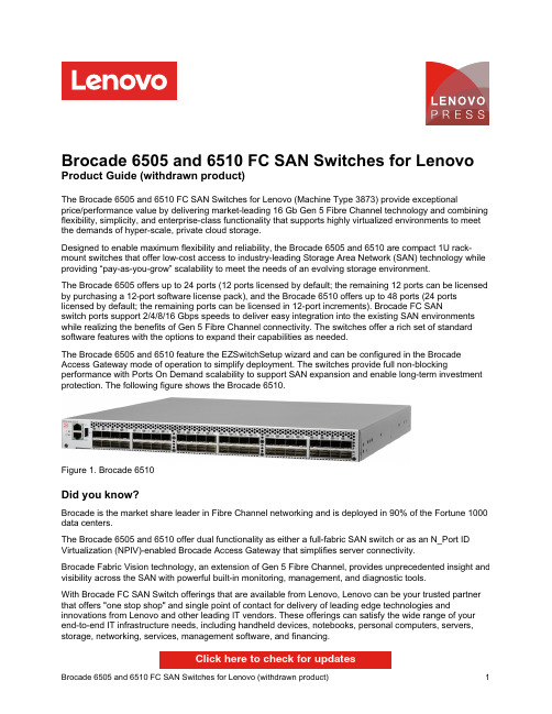
Brocade 6505 and 6510 FC SAN Switches for Lenovo Product Guide (withdrawn product)The Brocade 6505 and 6510 FC SAN Switches for Lenovo (Machine Type 3873) provide exceptionalprice/performance value by delivering market-leading 16 Gb Gen 5 Fibre Channel technology and combining flexibility, simplicity, and enterprise-class functionality that supports highly virtualized environments to meet the demands of hyper-scale, private cloud storage.Designed to enable maximum flexibility and reliability, the Brocade 6505 and 6510 are compact 1U rack-mount switches that offer low-cost access to industry-leading Storage Area Network (SAN) technology while providing “pay-as-you-grow” scalability to meet the needs of an evolving storage environment.The Brocade 6505 offers up to 24 ports (12 ports licensed by default; the remaining 12 ports can be licensed by purchasing a 12-port software license pack), and the Brocade 6510 offers up to 48 ports (24 ports licensed by default; the remaining ports can be licensed in 12-port increments). Brocade FC SANswitch ports support 2/4/8/16 Gbps speeds to deliver easy integration into the existing SAN environments while realizing the benefits of Gen 5 Fibre Channel connectivity. The switches offer a rich set of standard software features with the options to expand their capabilities as needed.The Brocade 6505 and 6510 feature the EZSwitchSetup wizard and can be configured in the Brocade Access Gateway mode of operation to simplify deployment. The switches provide full non-blocking performance with Ports On Demand scalability to support SAN expansion and enable long-term investment protection. The following figure shows the Brocade 6510.Figure 1. Brocade 6510Did you know?Brocade is the market share leader in Fibre Channel networking and is deployed in 90% of the Fortune 1000 data centers.The Brocade 6505 and 6510 offer dual functionality as either a full-fabric SAN switch or as an N_Port ID Virtualization (NPIV)-enabled Brocade Access Gateway that simplifies server connectivity.Brocade Fabric Vision technology, an extension of Gen 5 Fibre Channel, provides unprecedented insight and visibility across the SAN with powerful built-in monitoring, management, and diagnostic tools.With Brocade FC SAN Switch offerings that are available from Lenovo, Lenovo can be your trusted partner that offers "one stop shop" and single point of contact for delivery of leading edge technologies and innovations from Lenovo and other leading IT vendors. These offerings can satisfy the wide range of your end-to-end IT infrastructure needs, including handheld devices, notebooks, personal computers, servers, storage, networking, services, management software, and financing.Click here to check for updatesFigure 2. Brocade 6505Components and connectorsThe following figure shows the port-side view of the Brocade 6505.Figure 3. Brocade 6505 port-side viewThe following figure shows the port-side view of the Brocade 6510.Figure 4. Brocade 6510 port-side viewThe following figure shows the non-port side view of the Brocade 6505 and 6510.Figure 5. Brocade 6505 and 6510 non-port-side viewThe following table lists additional POD licenses for the Brocade 6505 and 6510. Table 3. POD license optionsDescription Partnumber FeaturecodeMax qtysupportedPOD software license for the Brocade 6505Brocade 6505 12 Port Software License Pack (POD)00MT457ASK51POD software license for the Brocade 6510Brocade 6510 12 Port Software License Pack (POD)00MT459ASK62If needed, the Brocade 6505 and 6510 can be mounted in a 2-post rack cabinet by using the optional mid-mount rack kit that is listed in the following table.Table 4. Rack-mount optionsDescription Part number Featurecode Max qty supportedLenovo B65xx Mid-mount Rack Kit00MY760ASKL1The optional mid-mount rack kit for the Brocade 6505 and 6510 is shown in the following figure.Figure 6. Lenovo B65xx Mid-mount Rack KitTransceivers and cablesThe Brocade 6505 and 6510 come without SFP+ media; SFP+ transceivers must be ordered together with the switch. The following table lists the supported SFP+ options and optical cables.Table 5. Supported SFP+ transceivers and optical cablesDescription Part number Featurecode Max qty supported (6505/6510)16 Gb FC SFP+ transceiversBrocade 16Gb SW SFP+ Optical Transceiver88Y6393A22R24 / 48 Brocade 16Gb 10km LW SFP+ Transceiver00MY768ASK224 / 48 Brocade 16Gb 25km ELW SFP+ Transceiver00MY770ASK324 / 48* 8 Gb FC SFP+ transceiversBrocade 8Gb SW SFP+ Optical Transceiver88Y6416508424 / 48 Brocade 8Gb 10km LW SFP+ Transceiver00MY764ASK024 / 48 Brocade 8Gb 25km ELW SFP+ Transceiver00MY766ASK124 / 48*Optical cables for 8 Gb and 16 Gb FC SW SFP+ transceivers Lenovo 0.5m LC-LC OM3 MMF Cable 00MN498ASR524 / 48Lenovo 1m LC-LC OM3 MMF Cable 00MN502ASR624 / 48Lenovo 3m LC-LC OM3 MMF Cable 00MN505ASR724 / 48Lenovo 5m LC-LC OM3 MMF Cable 00MN508ASR824 / 48Lenovo 10m LC-LC OM3 MMF Cable 00MN511ASR924 / 48Lenovo 15m LC-LC OM3 MMF Cable 00MN514ASRA 24 / 48Lenovo 25m LC-LC OM3 MMF Cable 00MN517ASRB 24 / 48Lenovo 30m LC-LC OM3 MMF Cable00MN520ASRC24 / 48Description Part numberFeature codeMax qty supported (6505/6510)* When using ELW SFP+ transceivers over distances over 10 km, the Extended Fabric feature is required on a SAN switch to drive the maximum bandwidth over the extended links (see Table 7 for ordering information).The following table lists the cabling requirements for the switch.Table 6. Brocade 6505 and 6510 cabling requirementsTransceiver CableConnector16 Gb Fibre Channel 16 Gb FC SW SFP+ ModuleUp to 30 m with fiber optic cables supplied by Lenovo (see Table 2); 850 nm OM4 multimode fiber (up to 125 m at 16 Gbps; up to 150m at 8 Gbps; up to 400 m at 4 Gbps); 850 nm OM3 multimode fiber (up to 100 m at 16 Gbps; up to 150 m at 8 Gbps; up to 380 m at 4Gbps)LC16 Gb FC LW SFP+ Module 1310 nm single-mode fiber cable (9 µ) up to 10 km LC 16 Gb FC ELW SFP+Module1310 nm single-mode fiber cable (9 µ) up to 25 kmLC8 Gb Fibre Channel 8 Gb FC SW SFP+ ModuleUp to 30 m with fiber optic cables supplied by Lenovo (see Table 2);850 nm OM3 multimode fiber (up to 150 m at 8 Gbps; up to 380 m at 4 Gbps; up to 500 m at 2 Gbps)LC 8 Gb FC LW SFP+ Module 1310 nm single-mode fiber cable (9 µ) up to 10 km LC 8 Gb FC ELW SFP+ Module 1310 nm single-mode fiber cable (9 µ) up to 25 km LC Management ports 10/100 Mb Ethernet management port UTP Category 5, 5E, and 6 up to 100 metersRJ-45RS-232 management portDB-9/RJ-45-to-RJ-45 console cable (comes with the switch)RJ-45Power supplies and cablesThe Brocade 6505 and 6510 support up to two redundant hot-swap 150 W AC power supplies. Each power supply has an IEC 309-C14 connector.The Brocade 6505 comes standard with one power supply, and the Brocade 6510 comes standard with two power supplies. The following table lists ordering information for the optional power supply for the Brocade 6505.Table 9. Power supply for the Brocade 6505.Description Partnumber Feature codeLenovo B6505 Redundant Power Supply00MY807ASKTThe switches come standard without a power cord; one or two rack power cables or line cords must be ordered together with the switch depending on the quantity of power supplies in the switch (see the following table).Table 10. Part numbers and feature codes for ordering power cordsDescription Partnumber Feature code1.5m, 10A/100-250V, C13 to IEC 320-C14 Rack Power Cable39Y793762011.8m, 10A/100-250V, 2xC13PM to IEC 320-C14 Rack Power Cable None*65682.8m, 10A/100-250V, C13 to IEC 320-C14 Rack Power Cable None*6311 2.8m, 10A/100-250V, C13 to IEC 320-C20 Rack Power Cable39Y79386204 4.3m, 10A/100-250V, C13 to IEC 320-C14 Rack Power Cable39Y79326263 10A/125V C13 to NEMA 5-15P 4.3m line cord39Y79316207 10A/250V C13 to NEMA 6-15P 2.8m line cord46M2592A1RF Argentina 10A/250V C13 to IRAM 2073 2.8m line cord39Y79306222 Australia/NZ 10A/250V C13 to AS/NZ 3112 2.8m line cord39Y79246211 Brazil 10A/125V C13 to NBR 6147 2.8m line cord39Y79296223 China 10A/250V C13 to GB 2099.1 2.8m line cord39Y79286210 Denmark 10A/250V C13 to DK2-5a 2.8m line cord39Y79186213 European 10A/230V C13 to CEE7-VII 2.8m line cord39Y79176212 India 10A/250V C13 to IS 6538 2.8m line cord39Y79276269 Israel 10A/250V C13 to SI 32 2.8m line cord39Y79206218 Italy 10A/250V C13 to CEI 23-16 2.8m line cord39Y79216217 Japan 12A/125V C13 to JIS C-8303 2.8m line cord46M2593A1RE Korea 12A/250V C13 to KETI 2.8m line cord39Y79256219 South Africa 10A/250V C13 to SABS 164 2.8m line cord39Y79226214 Switzerland 10A/250V C13 to SEV 1011-S24507 2.8m line cord39Y79196216 Taiwan 10A/250V C13 to CNS 10917-3 2.8m line cord00CG265A53E Taiwan 15A/125V C13 to CNS 10917-3 2.8m line cord00CG267A53F United Kingdom 10A/250V C13 to BS 1363/A 2.8m line cord39Y79236215 * Available for factory-built custom configurations and solutions only.Physical specificationsFC SAN tape backup unitsThe following table lists the external backup options that are offered by Lenovo that can be used in Brocade FC SAN solutions.Table 13. External backup optionsDescription Part number External tape backup librariesIBM TS3100 Tape Library Model L2U61732ULIBM TS3200 Tape Library Model L4U61734ULFibre Channel backup drives for TS3100 and TS3200 Tape Libraries6173 LTO Ultrium 5 Fibre Channel Drive00NA1076173 LTO Ultrium 5 Half High Fibre Drive Sled00NA1136173 LTO Ultrium 6 Fibre Channel Drive00NA1156173 LTO Ultrium 6 Half High Fibre Drive Sled00NA1196173 LTO Ultrium 7 Fibre Channel Drive00WF7656173 LTO Ultrium 7 Half High Fibre Drive Sled00WF769For more information, see the list of Product Guides in the Backup Units category:/servers/options/backupPower distribution unitsThe following table lists the power distribution units (PDUs) that are offered by Lenovo that can be used in Brocade FC SAN solutions.Table 17. Power distribution unitsDescription Part number0U Basic PDUs0U 12 C19/12 C13 32A 3 Phase PDU with IEC 309 3P+N+Gnd line cord46M4143 Switched and Monitored PDUs1U 9 C19/3 C13 Switched and Monitored DPI PDU (without line cord)46M40021U 9 C19/3 C13 Switched and Monitored 60A 3 Phase PDU with IEC 309 3P+Gnd line cord46M40031U 12 C13 Switched and Monitored DPI PDU (without line cord)46M40041U 12 C13 Switched and Monitored 60A 3 Phase PDU with IEC 309 3P+Gnd line cord46M40050U 24 C13 Switched and Monitored 30A PDU with NEMA L6-30P line cord46M41160U 12 C19/12 C13 Switched and Monitored 32A 3 Phase PDU with IEC 309 3P+N+Gnd cord46M41370U 12 C19/12 C13 Switched and Monitored 50A 3 Phase PDU with CS8365L 3P+Gnd cord46M4134Ultra Density Enterprise PDUs (9x IEC 320 C13 + 3x IEC 320 C19 outlets)Ultra Density Enterprise C19/C13 PDU Module (without line cord)71762NXUltra Density Enterprise C19/C13 PDU 60A/208V/3ph with IEC 309 3P+Gnd line cord71763NUC13 Enterprise PDUs (12x IEC 320 C13 outlets)DPI C13 Enterprise PDU+ (without line cord)39M2816DPI Single Phase C13 Enterprise PDU (without line cord)39Y8941C19 Enterprise PDUs (6x IEC 320 C19 outlets)DPI Single Phase C19 Enterprise PDU (without line cord)39Y8948DPI 60A 3 Phase C19 Enterprise PDU with IEC 309 3P+G (208 V) fixed line cord39Y8923Front-end PDUs (3x IEC 320 C19 outlets)DPI 30amp/125V Front-end PDU with NEMA L5-30P line cord39Y8938DPI 30amp/250V Front-end PDU with NEMA L6-30P line cord39Y8939DPI 32amp/250V Front-end PDU with IEC 309 2P+Gnd line cord39Y8934DPI 60amp/250V Front-end PDU with IEC 309 2P+Gnd line cord39Y8940DPI 63amp/250V Front-end PDU with IEC 309 2P+Gnd line cord39Y8935 Universal PDUs (7x IEC 320 C13 outlets)DPI Universal 7 C13 PDU (with 2 m IEC 320-C19 to C20 rack power cord)00YE443DPI Universal Rack PDU with US LV and HV line cords39Y8951DPI Universal Rack PDU with CEE7-VII Europe line cord39Y8952DPI Universal Rack PDU with Denmark line cord39Y8953DPI Universal Rack PDU with Israel line cord39Y8954DPI Universal Rack PDU with Italy line cord39Y8955DPI Universal Rack PDU with South Africa line cord39Y8956DPI Universal Rack PDU with UK line cord39Y8957DPI Universal Rack PDU with AS/NZ line cord39Y8958DPI Universal Rack PDU with China line cord39Y8959DPI Universal Rack PDU (Argentina)39Y8962Description Part number DPI Universal Rack PDU (Brazil)39Y8960DPI Universal Rack PDU (India)39Y8961NEMA PDUs (6x NEMA 5-15R outlets)DPI 100-127V PDU with Fixed NEMA L5-15P line cord39Y8905Line cords for PDUs that ship without a line cordDPI 32a Line Cord (IEC 309 3P+N+G)40K9611DPI 32a Line Cord (IEC 309 P+N+G)40K9612DPI 63a Cord (IEC 309 P+N+G)40K9613DPI 30a Line Cord (NEMA L6-30P)40K9614DPI 60a Cord (IEC 309 2P+G)40K9615DPI Australian/NZ 3112 Line Cord40K9617For more information, see the list of Product Guides in the Power Distribution Units category:/servers/options/pduUninterruptible power supply unitsThe following table lists the uninterruptible power supply (UPS) units that are offered by Lenovo that can be used in Brocade FC SAN solutions.Table 18. Uninterruptible power supply unitsDescription Part number RT1.5kVA 2U Rack or Tower UPS (100-125VAC)55941AXRT1.5kVA 2U Rack or Tower UPS (200-240VAC)55941KXRT2.2kVA 2U Rack or Tower UPS (100-125VAC)55942AXRT2.2kVA 2U Rack or Tower UPS (200-240VAC)55942KXRT3kVA 2U Rack or Tower UPS (100-125VAC)55943AXRT3kVA 2U Rack or Tower UPS (200-240VAC)55943KXRT5kVA 3U Rack or Tower UPS (200-240VAC)55945KXRT6kVA 3U Rack or Tower UPS (200-240VAC)55946KXRT8kVA 6U Rack or Tower UPS (200-240VAC)55948KXRT11kVA 6U Rack or Tower UPS (200-240VAC)55949KXRT8kVA 6U 3:1 Phase Rack or Tower UPS (380-415VAC)55948PXRT11kVA 6U 3:1 Phase Rack or Tower UPS (380-415VAC)55949PXFor more information, see the list of Product Guides in the Uninterruptible Power Supply Units category: /servers/options/upsLenovo Financial ServicesLenovo Financial ServicesLenovo Financial Services reinforces Lenovo’s commitment to deliver pioneering products and services that are recognized for their quality, excellence, and trustworthiness. Lenovo Financial Services offers financing solutions and services that complement your technology solution anywhere in the world.We are dedicated to delivering a positive finance experience for customers like you who want to maximize your purchase power by obtaining the technology you need today, protect against technology obsolescence, and preserve your capital for other uses.We work with businesses, non-profit organizations, governments and educational institutions to finance their entire technology solution. We focus on making it easy to do business with us. Our highly experienced team of finance professionals operates in a work culture that emphasizes the importance of providing outstanding customer service. Our systems, processes and flexible policies support our goal of providing customers with a positive experience.We finance your entire solution. Unlike others, we allow you to bundle everything you need from hardware and software to service contracts, installation costs, training fees, and sales tax. If you decide weeks or months later to add to your solution, we can consolidate everything into a single invoice.Our Premier Client services provide large accounts with special handling services to ensure these complex transactions are serviced properly. As a premier client, you have a dedicated finance specialist who manages your account through its life, from first invoice through asset return or purchase. This specialist develops an in-depth understanding of your invoice and payment requirements. For you, this dedication provides a high-quality, easy, and positive financing experience.For your region specific offers please ask your Lenovo sales representative or your technology provider about the use of Lenovo Financial Services. For more information, see the following Lenovo website:/us/en/landingpage/lenovo-financial-servicesRelated publications and linksTrademarksLenovo and the Lenovo logo are trademarks or registered trademarks of Lenovo in the United States, other countries, or both. A current list of Lenovo trademarks is available on the Web athttps:///us/en/legal/copytrade/.The following terms are trademarks of Lenovo in the United States, other countries, or both:Lenovo®BladeCenter®Flex SystemRackSwitchSystem x®ThinkServer®Other company, product, or service names may be trademarks or service marks of others.。
HDS存储VSP用户维护手册-v1.0
HDS 存储VSP 用户维护手册(2024年5月)目录一、设备维护 (3)1.1VSP配置信息 (3)1.2VSP系统架构 (3)1.3维护常用命令 (6)1.4VSP应急方案-上下电操作 (29)1.5设备巡检 (31)二、微码升级 (35)2.1微码升级的意义 (35)2.2微码升级的策略 (36)2.3微码升级的步骤 (36)三、故障处理 (40)3.1故障处理预案 (41)四、案例 (42)4.1硬盘更换步骤 (42)4.2CHA更换步骤 (45)4.3DKA更换步骤 (50)4.4CM更换步骤 (53)一、设备维护1.1 VSP配置信息1.2 VSP系统架构1.2.1 VSP系统架构图其系统架构采用了交换式架构,如下所示。
图2-1:VSP硬件技术架构1.2.2 VSP主要部件图2-2 VSP硬件主要部件图VSP的主要部件包括:✓前端卡(CHA):负责连接外部主机或存储交换设备,如小型机;✓后端卡(DKA):负责连接内部磁盘存储设备,如硬盘;✓数据缓存卡〔CPC):CHA访问后端磁盘时的数据缓存区域;✓内存条〔CM):CM的内存条;✓PCI-Express交换卡〔ESW〕:DKC数据交换控制卡;✓处理器板卡〔MPB〕:负责前端及后端数据的处理;✓磁盘〔HDD):存储设备的磁盘;✓备份盘〔Spare Disk〕:用作备份盘的磁盘;✓电池〔Battery):系统掉电时保存数据的电池;✓电源〔PS):系统供电及交换用的电源;✓风扇〔FAN):系统冷却用的风扇;✓控制台〔SVP):系统配置和管理监控的控制台〔一台笔记本电脑〕;✓线缆〔Cable〕:连接存储内部和外部各部件间的电缆;✓光纤接头〔SFP):光纤转换接头;1.2.3 VSP存储的磁盘分布图VSP的磁盘分布按照如下进行标识:HDDxyz_dd其中:xy=Cabinet〔盘柜〕;z=HDU number〔磁盘笼编号〕dd=HDD number〔磁盘编号〕图2-3:VSP磁盘位置图1.3维护常用命令当盘机出现故障,如磁盘、控制卡、电源、内存、电池到出现异常时,会产生SIM信息,同时盘时机根据故障的严重程度,将Message或Alarm灯亮起。
博科存储网络运维指导手册
博科存储网络运维指导手册V ERSION 1.02016年7月文档修订记录文档编号:标题博科存储网络运维指导手册摘要本文档是为博科存储网络定制的运维指导手册当前版本V1.0创建日期2016-7文档作者舒磊文件名称博科存储网络维指导手册.doc修改记录日期修改人编写者摘要目录文档修订记录.................................................................................................................................... I I 目录.................................................................................................................................................. I II 前言 (1)文档目的 (1)编写环境 (1)适用人员 (1)内容范围 (1)一、网络架构描述 (2)二、主要运维场景 (4)1.端口故障 (4)具体现象 (4)故障信息确认 (4)故障处理 (7)影响范围 (14)预计处理时间 (14)验证方案 (14)2.磁盘访问故障 (15)具体现象 (15)故障信息确认 (15)故障处理 (15)影响范围 (17)预计处理时间 (17)验证方案 (17)3.端口板故障 (18)具体现象 (18)故障信息确认 (18)故障处理 (19)影响范围 (20)预计处理时间 (20)验证方案 (21)4.引擎故障 (21)具体现象 (21)故障信息确认 (21)故障处理 (22)影响范围 (24)预计处理时间 (24)验证方案 (24)5.风扇故障 (24)故障信息确认 (24)故障处理 (26)影响范围 (26)预计处理时间 (27)验证方案 (27)6.电源故障 (27)具体现象 (27)故障信息确认 (27)故障处理 (28)影响范围 (29)预计处理时间 (29)验证方案 (29)7.CR故障处理过程及方法 (29)具体现象 (29)故障信息确认 (29)故障处理 (30)影响范围 (32)预计处理时间 (33)验证方案 (33)8.边缘交换机整机故障 (33)具体现象 (33)故障信息确认 (33)故障处理 (34)影响范围 (34)预计处理时间 (34)验证方案 (34)9.核心光纤交换机整机故障 (35)具体现象 (35)故障信息确认 (35)故障处理 (35)影响范围 (36)预计处理时间 (36)验证方案 (36)三、主要变更场景 (37)1.微码升级 (37)配置备份 (38)微码升级 (38)校验微码升级 (40)微码升级常见问题 (40)2.新设备上线 (43)3.新增ZONE配置 (62)4.修改CFG、ZONE、A LIAS的名字 (64)5.删除ZONE或Z ONE的成员 (65)7.交换机扩容 (69)补充命令介绍 (71)F RAMELOG --SHOW 指令: (71)F ABRICLOG --SHOW 指令: (72)前言文档目的此文档主要用于工行博科存储网络的日常变更操作、故障处理以及存储网络的规模扩展,帮助行内博科SAN岗维护人员快速定位修复故障、熟悉日常变更操作流程,以及提高博科SAN日常运维效率。
Brocade FC交换机Firmware升级指导手册V1.0(正稿)
文档信息:Brocade FC交换机Firmware升级指导手册目录1.背景描述 (3)2.功能描述 (3)3.升级环境 (3)4.升级前的准备 (3)5.升级流程 (4)6.升级步骤 (4)6.1.架设FT P服务器 (4)6.2.测试FTP服务器的连通性 (7)6.3.检查当前交换机的Firmware版本 (7)6.4.备份交换机的配置文件 (8)6.5.升级交换机的Firmware (8)6.6.核实升级后的Firmware版本 (12)1. 背景描述目前,公司中使用FC-SAN 存储架构的项目非常多,在该架构中基本都是使用Brocade 的FC 交换机。
不少项目都存在着Brocade FC 交换机Firmware 版本过旧的问题,需要将Firmware 版本升级至新版本。
因此,研究院系统整合实验室撰写本手册,供项目相关工程师参考使用。
2. 功能描述本手册旨在指导工程师正确的升级Brocade 品牌FC 交换机的Firmware 版本。
3. 升级环境Brocade 交换机升级用主机1Gb/s Ethernet以太交换机升级工作需要一台主机(服务器、工作站均可),安装Windows Server 2003或者Windows XP 操作系统。
主机通过非屏蔽双绞线连接到以太交换机,Brocade 交换机的网络管理口也要连接到以太交换机。
4. 升级前的准备准备相关软件:下载FtpServer 软件ftp://ftp105r:6789ak@/software/Brocade/FTPServer.rar下载Brocade的新版固件ftp://ftp105r:6789ak@/software/Brocade/v6.3.1c.zip5. 升级流程6. 升级步骤6.1. 架设FT P服务器1) 设置升级主机的IP地址,需设置与FC交换机的管理IP(默认为10.77.77.77)在同一个网段之内。
本手册例中所用FC交换机管理IP为192.168.200.210,所以设置主机IP为192.168.200.10。
BROCADE NETIRON MLX-4, MLX-8, MLX-16, MLX-32 说明书
高性能运营商以太网主要特性支持4、8、16、32插槽IPv4/IPv6/•MPLS/VRF的城域路由器先进的城域以太网第2层业务•采用Brocade Direct Routing(BDR)技术•的线速IPv4、IPv6和MPLS转发非MPLS环境中通过Multi-VRF实现的虚拟•路由行业领先的以太网和POS端口密度•全分布、无阻塞式架构,单系统容量高•达3.2 Tbps(每秒钟约20亿数据包转发能力)运营商级服务质量,支持融合的多重播•放网络高可用性设计提供冗余管理模块、交换•矩阵、电源、风扇、无中断故障切换和无中断软件升级通过POS接口或10-GbE WAN PHY接口灵•活地支持SONET/SDH非常适合于城域网(MAN)、互联网边•缘/聚合路由、大型数据中心、大型企业核心和高性能计算(HPC)领域的各种高级应用多业务IP/MPLS聚合路由器产品彩页网络规划人员必须确保所选的解决方案既要具备所需的功能和性能,同时还能降低总拥有成本(TCO)。
此外,可靠、面向未来的网络设计必须能适应技术的快速变化。
融合网络的日益普及使高可用性和服务质量(QoS)成了当今众多部署项目能否成功的关键。
在选择设备时,规划人员还需要确保,将来添加新功能时无需购买额外的硬件或软件。
Brocade® NetIron® MLX系列路由器能够满足所有上述及其它需求。
NetIron MLX系列路由器采用了基于第五代网络处理器的一流架构和太比特级交换矩阵,为网络规划人员提供了丰富的高性能IPv4、IPv6、MPLS 和Multi-VRF功能以及先进的第2层交换功能。
这些先进的交换路由器提供了广泛的功能,能够满足城域网、ISP、数据中心、大型企业、政府网络、教育/研究、高性能计算(HPC)等众多环境中的多样化需求。
NetIron MLX系列包括4插槽NetIron MLX-4、8插槽NetIron MLX-8、16插槽NetIron MLX-16、32插槽NetIron MLX-32四种型号。
瑞博华 200Ksps 12 位 32 通道 AD 4 通道 DA 板 4 通道脉冲计数 8 通道数
PCI总线200Ksps/12位32通道AD4通道DA板4通道脉冲计数8通道数字输入/8通道数字输出RBH7272使用说明书北京瑞博华控制技术有限公司二00七年十月200Ksps/12位32通道AD4通道DA板4通道脉冲计数(1个旋转编码器)8通道数字输入/8通道数字输出RBH7272使用说明书一、性能特点:本板采用PCI总线接口。
本板通过采用高速高精度AD芯片、高精度的仪器放大器、高密度CPLD逻辑芯片、精细地布线以及优良的制版工艺,实现了高速、高精度实时数据采集,具有以下性能特点:1、AD高精度:综合误差小于+/-1LSB 。
2、4通道脉冲功能:第一通道脉冲与第二通道脉冲可以构成一个旋转编码器输入,实时直接给出正向与反向脉冲数;第一通道同时输出脉冲的瞬态周期,时间分辨率为1微秒;第二、第三、第四通道输出16位的计数值,输入最高脉冲频率为采样频率×255,如采样频率10000,则输入最高脉冲频率为2.55MHz。
3、开关量同步采集输入:8路开关量与4路脉冲量合成第一通道与模拟量同步采集。
便于用户对开关量的高速采集。
可以用于外部同步触发等功能。
4、DA通道数:4通道独立锁存,精度12位5、AD高速度:多通道采集速度达到200Ksps(Sample Per Second),单通道方式也能够达到70Ksps以上,特别适合于工业控制中的数据采集。
6、程控放大器功能,可以设置放大倍数为1、2、4、8或1、10、100、1000。
7、AD硬件定时:板上提供硬件定时器,可以根据需要发出定时中断,采集软件在定时中断程序中采集,从而保证准确地时间基准,适于大部分的工业实时控制和高速数据采集的应用,特别是在WINDOWS95/98/2000的环境下,由于PC系统很难提供高精度的定时,采用本板的定时器,能够提供高精度的定时,同时能够实现高精度的数据采集,因此,在WINDOWS环境下采用本板具有特别的优点。
- 1、下载文档前请自行甄别文档内容的完整性,平台不提供额外的编辑、内容补充、找答案等附加服务。
- 2、"仅部分预览"的文档,不可在线预览部分如存在完整性等问题,可反馈申请退款(可完整预览的文档不适用该条件!)。
- 3、如文档侵犯您的权益,请联系客服反馈,我们会尽快为您处理(人工客服工作时间:9:00-18:30)。
1、概述
作为西藏移动业务支撑系统的核心光纤交换机,两台Sun SE48000/brocade 48000光纤交换机,因光纤模块端口不够,需利用其它48000交换机上的板卡进行扩容。
2、设备信息
主要涉及到4台48000,板卡为FC4-32
3、前期准备工作
3.1 备份原有数据
针对4台48K光纤交换进行数据备份,包括交换机信息、机框信息、板卡信息、电源信息、zone配置等。
switchshow
configshow
zoneshow
chassisshow
slotshow
psshow
firmwareshow
3.2打线缆标记
在操作前应将所有连接线缆打标签并登记,以便查询。
3.3 登记zone配置信息
详细登记zone配置信息
3.4 准备工具
螺丝刀、防静电纸、防静电手腕、交换机插槽挡板等
4、迁移过程
4.1 将空闲板卡踢出原交换机
检查空闲板卡是否有zone配置,如果有清除相应配置并重新应用zoneconfig配置。
在交换机switch admin配置界面,选择Blade项,对需要移除空闲板卡清除“Enable Blade”勾选等。
检查交换机监控管理界面,查看slot 8和9的状态
此处slot8和9的状态显示已踢出FC交换机。
4.2 关闭板卡电源
通过命令行登录光纤交换机,使用slotpoweroff命令关闭板卡电源
通过交换机管理监控界面,查看板卡状态
此时,两块板卡已从操作系统层面均踢出。
4.3 拔出空闲板卡
准备防静电纸、防静电手腕、螺丝刀等工具,到交换机前面准备拔出板卡。
A、开启交换机门
B、检查交换机电源指示灯、交换机引擎指示灯、板卡电源指示灯、光纤模块端口指示灯等,此时空闲板卡的电源指示灯为黄色,可以进行在线板卡插拔操作
C、拔出SFP线缆并做好线缆归类、捆绑等工作
D、利用板卡上方卡扣处的电源开关将板卡电源从物理层面关闭
E、用螺丝刀将板卡上下两颗螺丝拧松,并将卡扣剥离
F、将空闲板卡拔出交换机插槽,并轻放于防静电纸上
G、将交换机插槽挡板插入刚拔出的插槽
4.4 将空闲板卡插入BASS 48K交换机
A、用螺丝刀将插槽挡板上下螺丝拧松,并将挡板取出
B、将放在防静电纸上的空闲板卡插入插槽中,轻轻推入
C、板卡快推入到底的时候,停止推入,用双手分别按住板卡上下两个卡扣,轻轻使力将板推入插槽并固定住卡扣
D、用螺丝刀将上下两个螺丝拧紧
E、用手将板卡上方卡扣处的电源开关往上拔,知道通电位置
F、检查电源指示灯、端口指示灯等,电源指示灯亮绿灯、端口指示灯快速闪烁
G、用命令行模式登入交换机,检查状态
此时显示,新加的板卡正在自检
H、等POST过程完成后,检查板卡状态
I、登录交换机管理监控界面,查看日志
J、检查板卡端口状态
5、注意事项
如果插入板卡的微码版本低于交换机的,插入之后板卡自动从CP板download firmware。