Implementation of FPGA in the design of Embedded Systems
XGBE-XGXS-O4-N2中文资料
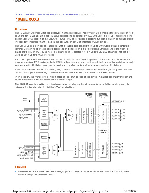
Home > Products > Intellectual Property > Lattice IP Cores > 10GbE XGXS10GbE XGXSOverviewThe 10 Gigabit Ethernet Extended Sublayer (XGXS) Intellectual Property (IP) Core enables the creation of system solutions for 10 Gigabit Ethernet (10 GbE) applications as defined by IEEE 802.3ae. This IP Core targets the pro-grammable array section of the ORCA ORT82G5 FPSC and provides a bridging function between 10 Gigabit Media Independent Interface (XGMII) and 10 Gigabit Attachment Unit Interface (XAUI) devices.The ORT82G5 is a high-speed transceiver with an aggregate bandwidth of up to 29.6 Gbits/s that is targeted towards users in need of high-speed backplane and chip-to-chip interfaces using Ethernet and Fibre-Channel based protocols. The ORT82G5 has eight channels of integrated 0.6-3.7 Gbits/s SERDES channels that can be used as 2x10 Gbits/s XAUI interfaces.XAUI is a high-speed interconnect that offers reduced pin count and is specified to drive up to 20 inches of PCB trace on standard FR-4 material. Each XAUI interface comprises four self-timed 8b/10b encoded serial lanes each operating at 3.125 Gbits/s and thus is capable of transferring data at an aggregate rate of 10 Gbits/s.XGMII is a 156MHz Double Data Rate (DDR), parallel, short-reach interconnect interface (typically less than two inches). It supports interfacing to 10Gb/s Ethernet Media Access Control (MAC) and PHY devices.In this design, the XGXS core is implemented in the FPGA portion of the device. A packet generator/checker and MDIO interface are also implemented in the FPGA logic.The XGXS IP core is provided with implementation scripts, test benches, and documentation to allow users to integrate the functions for 10 GbE LAN/WAN applications.FeaturesComplete 10Gb Ethernet Extended Sublayer (XGXS) Solution Based on the ORCA ORT82G5 0.6-3.7 Gbit/s 8b/10b Backplane Interface FPSC.IP Targeted to the ORT82G5 Programmable Array Section Implements Functionality Conforming to IEEEStandard 802.3ae, Including:10 GbE Media Independent Interface (XGMII).Slip buffers for clock domain transfer to/from the XGMII interface.Complete translation between XGMII and XAUI PCS layers, including 8b/10b encoding and decoding ofIdle, Start, Terminate, Error and Sequence code groups and sequences, and randomized Idle generation inthe XAUI transmit direction.64-bit data/8-bit control packet generator/checker on the XGMII side that supports standard compliantCRPAT and CJPAT generation and checking for XAUI interoperability testing.Standard compliant MDIO/MDC interface.Automatic initialization and synchronization of the embedded core.Interface with the high-speed SERDES block embedded in the ORT82G5 that implements a standard XAUI.XAUI Functionality Supported by the Embedded Portion of the ORT82G5, Including:Eight channels of 3.125 Gbits/s serializer/deserializer with 8b10b encoding/decoding (four SERDESchannels are used in this application).XAUI compliant lane-by-lane synchronization.Lane deskew functionality.Evaluation Configurations1 Results are generated with ispLEVER TM v.4.2 targeting ORT82G5-3, BM680. The numbers include wrapper logic.Ordering InformationPart Numbers:For ORCA 4: XGBE-XGXS-O4-N2To find out how to purchase the 10GbE XGXS IP Core, please contact your local Lattice Sales Office . Core Performance and Utilization 1Core Configuration ORCA4 PFUs LUTs Registers EBR Blocks PIO fMAX (MHz)xgbe_xgxs_o4_2_00294122475899484156。
vivado implementation策略
Vivado Implementation 策略Vivado 是由赛灵思公司(Xilinx)推出的一款集成电路开发工具,专门用于 FPGA/CPLD 的设计、仿真、调试和实现。
Vivado Implementation 策略指的是在使用 Vivado 进行 FPGA 设计时,针对不同的项目需求和目标硬件评台,制定合适的实现策略,以优化设计的性能、功耗和资源利用率。
下面我们来探讨一些常见的 Vivado Implementation 策略。
一、时序约束优化在 FPGA 设计中,时序约束的准确性对于设计的性能至关重要。
通过合理地设置时序约束,可以确保设计在目标时钟频率下能够正常工作,并且最大化地利用 FPGA 资源。
时序约束还可以帮助 Vivado 在实现过程中更好地优化逻辑综合和布局布线,进而提高设计的时序稳定性和抗干扰能力。
在进行 Vivado Implementation 时,需要仔细分析设计中的关键路径,准确设置时序约束,并根据需要进行时序优化,以达到设计的性能指标。
二、资源利用率优化在 FPGA 设计中,资源利用率优化是指在实现过程中最大化地利用FPGA 提供的逻辑单元、存储单元和 DSP 资源,以及减少设计对资源的竞争和冲突。
为此,在进行 Vivado Implementation 时,可以采取一些策略来优化资源利用率,例如合并逻辑、减少冗余逻辑、优化存储器结构、合理分配 DSP 资源等。
通过合理的资源利用率优化,可以有效降低设计的成本和功耗,提高设计的可靠性和稳定性。
三、功耗优化随着移动设备、物联网、人工智能等应用的不断发展,对于 FPGA 设计的功耗要求也越来越高。
在 Vivado Implementation 过程中,需要采取一些策略来优化设计的功耗。
可以通过减少逻辑单元、优化时钟管理、采用低功耗 IP 核等方式来降低设计的功耗。
还可以利用Vivado 提供的功耗分析工具来评估设计的功耗情况,进一步优化设计的功耗性能。
FPGA毕业设计论文英文
[1] Using FPGA technology towards the design of an adaptive fault tolerant frameworkErdogan, Sevki (University of Hawaii); Gersting, Judith L.; Shaneyfelt, Ted; Duke, Eugene L. Source: Conference Proceedings - IEEE International Conference on Systems, Man and Cybernetics, v 4, IEEE Systems, Man and Cybernetics Society, Proceedings - 2005 International Conference on Systems, Man and Cybernetics, 2005, p 3823-3827ISSN: 1062-922X CODEN: PICYE3Conference: IEEE Systems, Man and Cybernetics Society, Proceedings - 2005 International Conference on Systems, Man and Cybernetics, Oct 10-12 2005, Waikoloa, HI, United States Sponsor: IEEE Systems, Man and Cybernetics Society Publisher: Institute of Electrical and Electronics Engineers Inc.Abstract: In this paper we propose architecture for a Reconfigurable, Adaptive, Fault-Tolerant (RAFT) framework for application in real time systems with require multiple levels of redundancy and protection. Typical application environments include distributed processing, fault-tolerant computation, and mission and safety-critical systems. The framework uses Field Programmable Gate Array (FPGA) technologies with on the fly partial programmability achieving reconfiguration of a system component when the existing components fail or to provide extra reliability as required in the specification. The framework proposes the use an array of FPGA devices to implement a system that, after detecting an error caused by a fault, can adaptively reconfigure itself to achieve fault tolerance. The FPGAs that are becoming widely available at a low cost are exploited by defining a system model that allows the system user to define various levels of reliability choices, providing a monitoring layer for the system engineer. ? 2005 IEEE. (21 refs.)[2]METHOD FOR PROTECTING COMPUTER THROUGH REAL-TIME MONITORING BY PROTECTING EXECUTION FILE, AND COMPUTER AND SYSTEM PROTECTED BY THE SAMEPatent number: KR20040083409Publication date: 2004-10-01Inventor: AHN MU GYEONGApplicant: SAFEI CO LTDClassification:- international: G06F11/30; G06F11/30; (IPC1-7): G06F11/30- european:Application number: KR20040072633 20040910Priority number(s): KR20040072633 20040910View INPADOC patent familyView forward citationsReport a data error hereAbstract of KR20040083409PURPOSE: A method for protecting a computer through real-time monitoring, and the computer and a system protected by the same are provided to safely protect the computer by monitoring an interrupt or an event related to file handling and enable a user to perform setting conveniently. CONSTITUTION: A setting list(50) stores permission for changing an executable file. A detecting module(10) detects/intercepts occurrence of the interrupt or the event related to the file handling. An analysis module(20) checks the permission by comparing the interrupt or the event detected from the detecting module with the setting list after checking that the interrupt or the event is a request for changing the executable file by analyzing the interrupt or the event. A processing module(30) disuses or returns the interrupt or the event depending on an analysis result of the analysis module.[3] Method and system for protecting computer system from malicious software operationPatent number: US2004225877Publication date: 2004-11-11Inventor: HUANG ZEZHEN (US)Applicant:Classification:- International: G06F1/00; G06F11/30; G06F1/00; G06F11/30; (IPC1-7): G06F11/30 - European:Application number: US20040792506 20040303Priority number(s): US20040792506 20040303; US20030469113P 20030509View INPADOC patent familyView forward citationsAlso published as:CN1550950 (A)Report a data error hereAbstract of US2004225877A method and system for protecting a computer system from malicious software operations in real-time is disclosed. The security system combines system and user activity information to derive a user initiation attribute indicating whether or not a system operation is initiated by a computer user, and stop secrete malicious software operations that are not initiated by a computer user. The security system incorporates a plurality of attributes to support flexible security policy design, warn about potentially damaging operations by Trojan programs, and dynamically create security policies to allow trusted programs to perform trusted operations.[4]PREBOOT PROTECTION, IDENTIFICATION AND SECURITY OF A COMPUTER SYSTEMPatent number: WO0233522Publication date: 2002-04-25Inventor: TELLO JOSE ALBERTOApplicant: CODEX TECHNOLOGIES INC (CA)Classification:- international: G06F1/00; G06F21/00; G06F1/00; G06F21/00; (IPC1-7): G06F1/00; G06F9/445- european: G06F21/00N5A2D; G06F21/00N1C; G06F21/00N1V; G06F21/00N3P2 Application number: WO2000IB01659 20001017Priority number(s): WO2000IB01659 20001017; US199******** 19990104View INPADOC patent familyView forward citationsAlso published as:US6463537 (B1)Cited documents:WO0048063US5835597WO9613002US5610981WO9839701Report a data error hereAbstract of WO0233522A "personalized" computer with a unique digital signature which will not boot up or recognize any data storage or communication peripheral devices without a matching "personalized" smart card containing a complementary encrypted digital signature. A modified BIOS (Basic Input Output System) replaces the standard BIOS of a motherboard and allows a security engine microprocessor to take over preboot control of the computer from the motherboard CPU (Central Procesisng Unit), configures and operates the encryption-based security system, and enables or disables selected data storage devices and other user selectable peripherals upon start up and shut down of the computer. The enabling or disabling of peripheral devices involves the use of special enabling/disabling circuits. A modified DDL (Device Driver Layer), loaded in the hard drive of the computer as part of the resident O/S (Operating System) of the computer, and memory buffer circuits allows a real time encryption system to be in place for any communication or data storage device. A data encryption engine in the security engine microprocessor allows encryption and decryption of all data stored indata storage devices. Upon power up, reset or interrupt of the computer, the microprocessor looks for, and if present, reads from the smart card in the smart card reader which is logically connected to the security engine microprocessor. This invention can also be used to allow identification and authentication of the computer and its user in networks.[5]Temporarily authorizing the use of a computer programme protected by an electronic cartridgePatent number: GB2302968Publication date: 1997-02-05Inventor: ANTONINI PIERREApplicant: ANTONINI PIERRE (FR)Classification:- international: G06F21/00; G06F21/00; (IPC1-7): G06F1/00- european: G06F21/00N7P5HApplication number: GB199******** 19960701Priority number(s): FR199******** 19950705View INPADOC patent familyView forward citationsAlso published as:US5898778 (A1)FR2736448 (A1)DE19626972 (A1)Report a data error hereAbstract of GB2302968Use of a programme protected by an electronic cartridge in a computer system is authorised for a period limited by a number of hours or a date. So as to extend the use of a protected programme contained in the memory (103) of the computer system (100-106), the user needs to enter by means of the keyboard (105) into this system a password so as to reset the electronic cartridge (107). This electronic cartridge (107) preferably comprises a memory (108), a first counter (110), a second counter (112), a monostable element (113), an adder (114), a real time clock (109) and a cabled logic network (111). This device is connected to the outside of the computer system (100-106) by means of a connector. For renting software, this invention is able to control the use of these programmes.[6] System for computer software protectionPatent number: US5666411Publication date: 1997-09-09Inventor: MCCARTY JOHNNIE C (US)Applicant:Classification:- international: G06F1/00; G06F9/38; G06F21/00; G06F1/00; G06F9/38; G06F21/00; (IPC1-7): H04L9/00- european: G06F21/00N7P5H; G06F9/38S4L; G06F21/00N1C1Application number: US199******** 19940113Priority number(s): US199******** 19940113View INPADOC patent familyView forward citationsReport a data error hereAbstract of US5666411This system protects proprietary software from disclosure and unauthorized use, enforces license limits on number of users of the software, and prevents corruption of protected software by computer viruses. Software protected under this system may execute only on computer systems which incorporate a microprocessor capable of deciphering enciphered instructions in real time. Program files are first enciphered under control of a distribution cipher key. Prior to first use of software, program files must be customized on the user computer system. This customization procedure re-enciphers the programs, so that they are enciphered under a second cipher key. Customized programs may not execute on a computer system other than one constructed with a processor chip which incorporates a crypto microprocessor. The crypto microprocessor is capable of performing this re-encipherment, and of executing both enciphered and unenciphered programs. The customization program runs on user's computer system and normally accesses a remote Exchange database system by means of a modem to accomplish its task. Variations of customization process provide for storage of enciphered software on either a single system, a network server, or a site license repository system.[7]METHOD AND DEVICE FOR PROTECTION OF COMPUTER SYSTEM FROM ILLEGAL DISTRIBUTIONPatent number: BG48653Publication date: 1991-04-15Inventor: KOLEV VLADIMIR N (BG); MARDIROSJAN GARO KH (BG) Applicant: TS LAB KOSM IZSLEDV ANIJAClassification:- international: G06F5/00; G06F5/00; (IPC1-7): G06F5/00- european:Application number: BG198******** 19890712Priority number(s): BG198******** 19890712View INPADOC patent familyView forward citationsReport a data error hereAbstract of BG48653The invention is designed for the production and use of computer systems and their software. It provides complete protection against undesirable unauthorised copying and reproduction. The method of current real time of the computer system serves to establish a protection code combination for the software product currently used by it. The unit consists of a power supply unit (1), a quartz crystal standart (2), a real time register (3), a real time coder (4), a protection code register (5) and an interface package (6)[8]DEVICE FOR PROTECTING INFORMATION BY USING USB SECURITY MODULE ON BASIS OF PC AND CODE CHIPPatent number: KR20010048160Publication date: 2001-06-15Inventor: CHO JIN HO (KR); CHOI KWANG YUN (KR); HAN SEUNG JO (KR) Applicant: CHO JIN HO (KR); CHOI KWANG YUN (KR); HAN SEUNG JO (KR); SOFTPROTEC CO LTD (KR)Classification:- international: H04L9/00; H04L9/00; (IPC1-7): H04L9/00- european:Application number: KR199******** 19991125Priority number(s): KR199******** 19991125View INPADOC patent familyView forward citationsReport a data error hereAbstract of KR2001004816PURPOSE: A device for protecting information by using a USB security module on basis of a PC and a code chip is provided to prevent illegal copy and modification of the software or data by the illegal users on the basis of the PC and to protect the important data and information. CONSTITUTION: The device for protecting information by using a USB(Universal Serial Bus) security module on basis of a PC and a code chip includes a USB controller(10) and a code chip(100). The USB controller(10) is composed of a USB core(11) and an MCU(12). The serial data by the outer input by using the USB port are sent in the USB core(11) and are in/output serially after buffering. If all the input data are the module information request order languages, the module information is read from a PROM(103) of the code chip(100) and is output to the input step of the USB core(11) or the 17 bites are output to the input step of a buffer(101) in the code chip(100) or the 16 bites input from thebuffer(101) are input and output to the input step of the USB core(11) in the MCU(12). The code chip(100) is composed of the buffer(101), a KSE96 block(110), a controlling portion(130), a mode checker(102), a scrambler, the PROM(103) and an RSA calculating portion(140).[9] Security method for protecting a system, e.g. a computer or online system against unauthorized access, whereby a computer is used with a chip card reader, with an additional varying control question used for access authenticationPatent number: DE10218945Publication date: 2003-11-13Inventor: SCHWENK JOERG (DE); SAAR EV A (DE)Applicant: DEUTSCHE TELEKOM AG (DE)Classification:- international: G06F21/00; G07F7/10; G06F21/00; G07F7/10; (IPC1-7): G06F17/60 - european: G06F21/00N5A2D; G07F7/10D6K; G07F7/10D6PApplication number: DE20021018945 20020422Priority number(s): DE20021018945 20020422View INPADOC patent familyView forward citationsReport a data error hereAbstract of DE10218945Method for securing a system against unauthorized access, whereby an input device is used to input a value that is compared with a stored input code in order to provide access to a system. Following input of the code, e.g. a PIN, a further control question is asked via a system output unit, e.g. the monitor. The question includes information for providing the answer and the user must input the correct answer before access is granted. The invention also relates to a system for implementing the method that comprises a computer with a chip card reader. The information displayed in the additional control question changes each time an identification chip card is inserted in the reader.[10]Computer chip heat protection apparatusPatent number: US6496118Publication date: 2002-12-17Inventor: SMITH WARREN L (US)Applicant:Classification:- international: H01L23/34; H01L23/467; H01L23/34; (IPC1-7): G08B17/00- european: H01L23/34; H01L23/467Application number: US20010953001 20010911Priority number(s): US20010953001 20010911View INPADOC patent familyView forward citationsReport a data error hereAbstract of US6496118A heat protection apparatus includes a heat sink adapted for mounting to a computer chip for dissipating heat generated thereby, the heat sink having a base defining a channel peripherally thereabout. A cooling fan is mounted to the heat sink for dispersing the dissipated heat. The apparatus includes a logic circuit capable of evaluating resistance input data and capable of energizing an alarm upon a programmed condition. The apparatus includes a temperature sensitive polymeric tape spanning between a pair of conductors connected to the circuit. The conductors and polymeric tape are mounted in the channel. The circuit energizes the alarm if the resistance data indicates a temperature greater than a predetermined critical temperature parameter or if the data indicates a temperature rate of rise greater than a critical rate of rise parameter. The alarm may be audible or provide a visual indicator to a computer display.[11] Protection device for portable computersPatent number: US2005039502Publication date: 2005-02-24Inventor: A VGANIM MAIR (IL)Applicant:Classification:- international: G06F1/00; G06F21/00; G06F1/00; G06F21/00; (IPC1-7): E05B73/00 - european: G06F21/00N5A2D; G06F21/00N1Z; G06F21/00N5A2BApplication number: US20040497635 20040602Priority number(s): IL20010146897 20011204; WO2002IL00965 20021202View INPADOC patent familyView forward citationsAlso published as:WO03048907 (A3)WO03048907 (A2)AU2002365735 (A1)Report a data error hereAbstract of US2005039502A protection device (16) particularly for portable computers (10) having a Universal Serial Bus (USB) socket (12) and a standardized dedicated slot (14) formed in vicinityof the socket (12). A key or the like operable mechanism (18) is provided for rotatinga T-shaped tip member (20) which is adapted to be inserted into and locked by the slot(14). Plug (22) may be either a "demo" or part of an active device, which functions to enable/disable the operation of the computer. The device (16) may further be provided with arresting means in the form of a cable (24), which can be tied to an immovable object such as table leg (26) for protecting the computer (10) against theft.[12] Electronic system and corresponding method for protecting an access gate of a computerPatent number: EP1429226Publication date: 2004-06-16Inventor: NICCOLINI MARCELLO (IT)Applicant: INFOTRONIC SPA (IT)Classification:- international: G06F21/00; G06F21/00; (IPC1-7): G06F1/00- european: G06F21/00N1V3Application number: EP20020425770 20021213Priority number(s): EP20020425770 20021213View INPADOC patent familyView forward citationsView document in the European RegisterCited documents:EP1248179WO9743716US6009527Report a data error hereAbstract of EP1429226The invention relates to a system and a method for protected access to an input/output gate (2) of an electronic processor equipped with conventional microprocessor units, volatile and mass memory units, at least one display unit, and an operating system (4) arranged to handle the several processor units, said access gate (2) being a USB gate allowing connenction at fast receptacle to predetermined peripheral units (3) of the electronic processor that are entitled to accede to be plugged in. The method comprises the following steps: detecting, through the operating system (4), the type of any unit coupled to said USB gate (2); comparing the detected type with a stored list of the predetermined units (3) entitled to accede; disabling the USB gate (2) if the comparison gives negative result.[13]APPARATUS FOR PROTECTING COMPUTER USING FUNCTIONAL CHARACTERPatent number: WO03072451Publication date: 2003-09-04Inventor: LEE IN JA (KR)Applicant: LEE IN JA (KR)Classification:- international: B65D41/26; B65D51/24; B65D81/36; B65D41/02; B65D51/24; B65D81/00; (IPC1-7): B65D41/26- european: B65D41/26; B65D51/24L; B65D81/36D2Application number: WO2002KR00432 20020313Priority number(s): KR20020005975U 20020228View INPADOC patent familyView forward citationsAlso published as:AU2002239122 (A1)Cited documents:KR890016287UKR880016247UReport a data error hereAbstract of WO03072451The present invention relates to a apparatus for protecting computer for notifying the outside of each of operation state of virus inspection using the character apparatus connected to the computer. The present invention includes computer for generating and transmitting the USB code value corresponding to registry value inspected from each of operation state of vaccine engine, and character apparatus for inquiring and outputting the voice data corresponding to the USB code value received from the computer. Hence, the present invention has an effect on not only hearing the information to virus inspection through the voice irrespective of the time as it always surveys the vaccine engine, but also presenting a fine view around the computer and increasing the effective value of the character by forming the character apparatus as the character including a doll.[14] Multiple protecting system to protect personal computer data from burglary utilized flash memory drivePatent number: US2003079140Publication date: 2003-04-24Inventor: URA YOSUKE (JP)Applicant:Classification:- international: G06F21/00; G06F21/00; (IPC1-7): H04L9/00- european: G06F21/00N1D1; G06F21/00N1V3Application number: US20010002501 20011024Priority number(s): US20010002501 20011024View INPADOC patent familyView forward citationsReport a data error hereAbstract of US2003079140This invention provides the system to protect the data stored in personal computer from burglary. This invention features providing method to protect the data stored in personal computer from easy burglary by combining several types of protecting method in the system that data is input and output inserting flash memory drive into USB port on personal computer.[15]Secure general purpose input/output pins for protecting computer system resourcesPatent number: US6138240Publication date: 2000-10-24Inventor: TRAN ROBIN T (US); SIMONICH CHRISTOPHER E (US) Applicant: COMPAQ COMPUTER CORP (US)Classification:- international: G06F21/00; G06F21/00; (IPC1-7): G06F11/00- european: G06F21/00N1VApplication number: US199******** 19980619Priority number(s): US199******** 19980619View INPADOC patent familyView forward citationsReport a data error hereAbstract of US6138240A security device and methodology that prevents unauthorized access to general purpose I/O pins in a computer system. In a system according to the invention, secure general purpose I/O pins are utilized as enable signals for data transfer devices such as Universal Serial Port (USB) ports. In one embodiment of the invention, access to the secure general purpose I/O pins is governed by an administrator password that is protected by a memory slot in a security device. When an administrator (or other authorized user) desires access to the general purpose I/O register that controls the secure general purpose I/O pins, the administrator enters the administrator password. If the password is correct, the relevant slot of the security device is unlocked, thereby permitting completion of write cycles to the secure general purpose I/O register. If a write cycle to the secure general purpose I/O register is attempted while the relevantslot in the security device is locked, the write cycle is ignored. Control and monitoring of various system resources in a secure manner is thereby permitted via use of the secure general purpose I/O pins.[16] SECRECY-PROTECTING COMPUTER AND PROGRAMPatent number: JP2006338136Publication date: 2006-12-14Inventor: KANEUCHI HIDEApplicant: MITSUBISHI ELECTRIC INF TECHClassification:- international: G06F21/24; H04L9/32; G06F21/00; H04L9/32;- european:Application number: JP20050159474 20050531Priority number(s): JP20050159474 20050531View INPADOC patent familyView forward citationsReport a data error hereAbstract of JP2006338136PROBLEM TO BE SOLVED: To provide a secrecy-protecting computer which prevents a file from being operated in a computer except the computer from which the file is taken away.SOLUTION: When a file is closed by a filter driver provided between an I/O manager and a device driver, plain-sentence data 100 to be stored are encrypted, and the file is stored in a form of mixed data 130 which include the encrypted data and a MAC address 120 unique to the computer. When the file is opened, the encrypted data included in the mixed data are decrypted only when the MAC address included in the mixed data 130 accords with a MAC address 130 unique to the computer which opens the file.[17] ACCESS PROTECTION FOR A COMPUTER BY MEANS OF A PORTABLE STORAGE MEDIUMPatent number: WO2006074490Publication date: 2006-07-13Inventor: FUCHS HJALMAR DOUGLAS (ZA)Applicant: FUCHS HJALMAR DOUGLAS (ZA)Classification:- international: G06F21/20; G06F21/20;- european:Application number: WO2005ZA00176 20051130Priority number(s): ZA20040009657 20041130View INPADOC patent familyView forward citationsCited documents:WO03079163US6401205DE19508288NL9101506FR2783943Report a data error hereAbstract of WO2006074490This Invention relates to a memory device such as a memory stick with a unique identifier or ID to be used in conduction with an electronic device such as a Personal Computer as to enable a user to gain access or operate or control devices or services associated with the electronic device for example a PC or Laptop. The systems software running or operational on the electronic device and/or memory device will search and read a unique identifier on the memory device such as a serial number or code. Should the serial number or code not be Read operation of the electronic device is seized.[18]METHOD AND SYSTEM FOR PROTECTING AGAINST COMPUTER VIRUSESPatent number: WO2005008417Publication date: 2005-01-27Inventor: KWAN TONY (AU)Applicant: COMPUTER ASS THINK INC (US); KWAN TONY (AU) Classification:- international: G06F21/00; G06F21/00; (IPC1-7): G06F- european: G06F21/00N3P; G06F21/00N3V6; H04L29/06C6HApplication number: WO2004US22216 20040709Priority number(s): US20030486754P 20030711View INPADOC patent familyView forward citationsView document in the European RegisterAlso published as:WO2005008417 (A3)EP1644859 (A3)EP1644859 (A2)EP1644859 (A0)Cited documents:US5956408US6049671US2003084322US5948104US2003065926more >>Report a data error hereAbstract of WO2005008417A method for delivering an update to at least one user including creating an electronic communication including an update and a unique signature identifying, the electronic communication as including the update and sending the electronic communication to the user..[19] Systems, methods, and computer program products for privacy protection Patent number: US2003130893Publication date: 2003-07-10Inventor: FARMER BENNIE L (US)Applicant: TELANON INC (US)Classification:- international: (IPC1-7): G06F17/60- european: G06F21/00N9A2P1Application number: US20020291196 20021108Priority number(s): US20020291196 20021108; US20000638177 20000811; US20010337827P 20011108View INPADOC patent familyView forward citationsReport a data error hereAbstract of US2003130893A systems and method of transmitting or communicating unique data from a unique user through a communications and/or computer network to a third party, wherein the third party has no method of determining the personal-identifying information (PII) of the unique user upon receiving the data. The invention provides privacy protection and location for communication of data, voice orOther information via a communications network, for providing various services related to telemetric communications and other location-based services.[20]Method and apparatus for establishing computer configuration protection passwords for protecting computer configurationsPatent number: US6470454Publication date: 2002-10-22Inventor: CHALLENER DA VID CARROLL (US); ATKINS BARRY DOUGLAS (US); ARNOLD TODD W (US)Applicant: IBM (US)Classification:- international: G06F21/00; G06F21/00; (IPC1-7): G06F11/30; H04L9/00; H04L12/14- european: G06F21/00N5A2Application number: US199******** 19980331Priority number(s): US199******** 19980331View INPADOC patent familyView forward citationsReport a data error hereAbstract of US6470454A method and apparatus is provided for facilitating the generation and use of computer system configuration passwords which can be utilized in an enterprise or organization to allow authorized users having knowledge of the password associated with a particular data processing system to make and change configuration decisions, but which prevents unauthorized users from making and changing such configuration decisions. In the preferred embodiment, a unique identifier (such as a serial number) and an enterprise secret key are supplied to a one-way cryptographic hash function in order to generate the configuration passwords which are unique to each data processing system of the plurality of data processing system of the enterprise or organization.。
2FSK调制解调系统的FPGA设计与实现

第38卷第3期2010年6月浙江工业大学学报J OURNAL OF ZH E J IAN G UN IV ERSIT Y OF TECHNOLO GYVol.38No.3J un.2010收稿日期:2009209215作者简介:应亚萍(1966—),女,浙江东阳人,实验师,硕士研究生,主要从事电子和通信等方向的研究,E 2mail :yyp825@.2FS K 调制解调系统的FP GA 设计与实现应亚萍,许建凤,陈婉君(浙江工业大学之江学院,浙江杭州310024)摘要:FS K (Frequency Shift Keying )———移频键控,或称数字频率调制,是数字通信中使用较早的一种调制方式.数字频率调制的基本原理是利用载波的频率变化来传递数字信息.在数字通信系统中,这种频率变化不是连续而是离散的.详细介绍了基于FP GA 的2FS K 调制解调系统的原理、设计、实现和调试,通过Quart us Ⅱ软件,在FP GA 实验板上设计了一种全数字2FS K 调制解调系统,并调试出结果.根据调试结果做出的优化设计,能够简化传统调制器的设计,缩短系统设计周期.关键词:2FS K;FP GA ;Quart us Ⅱ;HDL 中图分类号:TN914.3 文献标识码:A文章编号:100624303(2010)0320282204Design and implementation of 2FSK modulation 2demodulationsystem based on FPGAYIN G Ya 2ping ,XU Jian 2feng ,C H EN Wang 2jun(Zhijiang College ,Zhejiang University of Technology ,Hangzhou 310024,China )Abstract :FS K —Frequency Shift Keying ,or digital f requency modulation ,is an earlier modulation mode used in digital co mmunication.The basic principle of digital frequency modulation is using t he changes of carrier frequency to t ransmit digital information.In digital communication systems ,t he changes of f requency are not continuous but discrete.The paper int roduces t he principle ,design ,implementatio n ,and debug p rocess of t he 2FS K modulation 2demodulation system based on FP GA in details.U nder t he software of Quart us Ⅱ,a kind of digital 2FS K modulation 2demodulation system is designed o n t he FP GA experiemental board and t he debugged result s are achieved.The debugged result s can be used to optimize t he system design ,simplify t he design of t raditional modulator 2demodulator ,and shorten t he period of system design.K ey w ords :2FS K;FP GA ;Quart us Ⅱ;HDL 随着数字技术日益广泛的应用,以现场可编程门阵列FP GA 为代表的器件得到了广泛的应用,器件的集成度和速度都在高速增长.FP GA 既具有门阵列的高逻辑密度和高可靠性,又具有可编程逻辑器件的用户可编程性.它的可编程特性带来了电路设计的灵活性,在数字电路设计中发挥着越来越重要的作用.在通信系统中,基带数字信号在远距离传输,特别是在有限带宽的高频信道如无线或光纤信道上传输时,必须对数字信号进行载波调制.FS K 就是用数字信号去调制载波的频率,是信息传输中使用较早的一种调制方式.具有抗噪声性能好、传输距离远、误码率低等优点[1].在中低速数据传输中,特别是在衰落信道中传输数据时,有着广泛的应用[2].针对传统用硬件实现FS K 的方法,特别是相干解调需要提取载波,设备相对复杂、成本较高的特点,研究了基于FP GA 芯片的调制解调系统.通过Quart us II 软件平台,采用硬件描述语言,提出了一种2FS K 调制解调系统的设计实现方法,重点研究非相干的过零检测解调算法的实现.1 2FSK 调制解调原理及系统设计1.1 2FSK 调制解调原理2FS K 信号是用载波频率的变化来表征被传信息的状态的,被调载波的频率随二进制序列0,1状态而变化,即载频为f 1时代表传0,载频为f 2时代表传1.显然,2FS K 信号完全可以看成两个分别以f 1和f 2为载频,以a n 和a n 为被传二进制序列的两种2AS K 信号的合成.2FS K 信号的产生通常有两种方式:(1)频率选择法;(2)载波调频法.频率选择法是在二进制基带脉冲的控制下通过开关电路对两个不同的独立频率源进行选通.实现比较简单,获得了广泛应用.载波调频法是采用模拟调频电路来实现.在这里,采用的是频率选择法.2FS K 信号的常用解调方法可采用非相干检测法和相干检测法,实现比较复杂.此外,2FS K 信号还有其他解调方法,比如鉴频法、过零检测法及差分检波法等.过零检测法的原理框图如图1.图1 2FS K 键控信号的过零检测法解调原理框图Fig.1 The zero assay of 2FSK输入的已调信号经限幅放大后成为矩形脉冲波,再经微分电路得到双向尖脉冲,然后整流得到单向尖脉冲,每个尖脉冲表示信号的一个过零点,尖脉冲的重复频率就是信号频率的2倍.将尖脉冲去触发一个单稳态电路,产生一定宽度的矩形脉冲序列,该序列的平均分量与脉冲重复频率成正比,即与输入频率信号成正比.所以经过低通滤波器输出平均量的变化反映了输入信号的变化,这样就完成了频率—幅度变换,把码元“1”与“0”在幅度上区分开来,恢复出数字基带信号[3].1.2 2FSK 调制解调系统设计2FS K 调制解调系统框图如图2.输入时钟通过分频器1得到载波f 1的时钟,通过分频器2得到载波f 2的时钟,电路中设计两个载波映射表,根据时钟输入频率的不同,将A/D 正弦转换表映射成频率不同的载波f 1和f 2.设计5阶伪随机m 序列模块,用于产生基带信号.通过二选一数据选择器完成载波频率选择,生成2FS K 调制信号.图2 2FS K 调制解调系统图Fig.2 The modulation and demodulation system diagramof 2FSK已调信号经外部DA 转换芯片DAC0832转换为模拟信号,经信道传输,在接收端采用模数转换芯片MX7821采样,得到已调数字信号序列.系统解调电路采用过零检测法,不同的载波对应的零点数不同,过零点数反映了载波变化的不同,也反映了信码的不同.根据过零解调原理,解调模块包括正弦波限幅整形模块、微分整流模块、脉冲展宽模块、低通滤波模块以及抽样判决模块等子模块.为使解调部分的时钟信号与调制部分同步,加入了位同步dpll 模块,控制解调部分的抽样判决时钟.2 2FSK 调制电路的FPGA 实现2.1 m 序列生成在通信系统中,伪噪声序列(即PN 序列)得到了广泛的应用.最常用的PN 序列是最大长度线性码序列,又称为m 序列,是由n 级线性反馈移位寄存器产生的最大周期(2n -1)非零序列,其特点是具有周期性和伪随机性.m 序列是由带线性反馈的移位寄存器产生的周期最长的一种二进制序列.线性反馈移位寄存器的一般由移位寄存器,若干模二加法器组成线性反馈逻辑网络和时钟脉冲产生器连接而成.・382・第3期应亚萍,等:2FSK 调制解调系统的FP GA 设计与实现系统选用m 序列的阶数为5,五阶m 序列的本原多项式为g (x )=x 5+x 2+1.序列生成器采用D 触发器和门电路组成,如图3.异或门XOR 为线性反馈电路,门电路OR5和NO T 确保状态全零时系统能自启动.图3 m 序列电路图Fig.3 m sequence diagram2.2 正弦载波信号系统采用f 1和f 2两种不同频率正弦波,两者频率相差一倍.载波f 1和f 2通过查找A/D 映射表产生,每个正弦周期取16点采样.载波映射表由两个模块组成,分别是f1_zb.v 和f2_zb.v ,每个模块又调用下面的两个子模块rom.v 和sin16.mif ,其中rom.v 由Quart us II 开发环境的MegaWizard Plug 2In Manager 工具产生.表数据文件sin16.mif 的产生方法很多,可以在simulink 中的正弦波发生器后接示波器,然后把示波器的数据保存到workspace 中,再将数据填入用Quart us II 建立的mif 文件中.设计采用matlab 编程方法直接生成sin16.mif 文件,程序如下:x =0:1:15;y =ro und (1273sin (23pi 3x/16))+128;A =[x ;y ];fid =fopen (’C :\sin16.mif ’,’w ’);fprintf (fid ,’width =8;\r\n depth =16;\r\n ’);fp rintf (fid ,’address_radix =dec ;\r\n data_radix =dec ;\r\n ’);fp rintf (fid ,’content begin\r\n ’);fp rintf (fid ,’%d :%d ;\r\n ’,A );fp rintf (fid ,’end ;’);fclose (fid );plot (x ,y )plot 命令产生取值量化后的16点正弦波形.2.3 调制电路实现调制电路的实现采用模块化设计,对系统时钟计数分频,分频器div8和div16产生频率相差一倍 的时钟;m5模块产生五阶m 序列;mux 模块检测m5模块输出的跳变,当基带信号m 序列变化时,mux 模块根据m 序列值选择f 1或f 2频率的载波输出,完成基带信号的调制.3 2FSK 解调电路FPGA 实现3.1 解调电路实现解调电路系统接收模拟信号,经A/D 转换芯片mx7821采样得到数字信号;在zx 模块中进行限幅处理,得到方波信号;微分整流模块wf 进行边沿检测;pluse 模块负责脉冲展宽;lpf 模块为低通滤波器,得到待判决基带信号.低通滤波后的信号输入到同步模块中,提取位同步时钟信号,供给判决模块使用.最后,在同步时钟控制下进行判决得到解调后的基带信号.3.2 位同步设计解调系统中,需要对接收码元做位同步,目的是使每个码元得到最佳的解调和判决.设计利用FP 2GA 实现位同步,超前—滞后数字锁相环DPLL 的原理框图如图4所示.图4 位同步原理图Fig.4 Bit synchronization schematic diagram数字锁相环电路主要是由鉴相器、序列滤波器、可控分频器和时钟源组成,完成对输入定时信号提取、数字滤波和定时综合.其中可控分频器模值设计为N +1,N ,N -1三种;序列滤波器受鉴相器的输出控制.鉴相器采用的是微分型导前—滞后型鉴相器.时钟源使用系统时钟.锁相环的算法如图5所示.当提取位同步基准脉冲后,锁相环读取表示位同步脉冲可变模分频器的相位计数值,如果相位差在0~8(可调整,与锁相环参数有关)之间,则加大或减小分频器模值存储器,如果相位差为零,则为同步状态,保持原来的分频器模值大小.经过调整,可以使本地振荡器的相位与从线路码提取的位同步基准脉冲同相.・482・浙江工业大学学报第38卷图5 位同步锁相环算法图Fig.5 Bit synchronization phase 2locked loop algorithm4 2FSK 调制解调系统仿真及硬件配置为了整体观察调制解调过程是否正确,将各调制和解调模块组成电路,完成整个系统的电路设计.系统仿真波形图如图6.信号mo ut 为输出基带m 序列;zx 信号输出为限幅后的矩形脉冲;微分整流信号wf 检测信号的过零点,可以通过wf 信号观察到频率的变化;p ulse 为脉冲展宽信号,输出为一定宽度的矩形脉冲序列,该序列的平均分量与脉冲重复频率成正比,即与输入频率信号成正比;bsyn 为位同步定时;dout1信号为判决输出.通过仿真分析,判决输出dout1与发送基带信号mout 一致,但由于信号处理过程产生了一定的延时.设计好的电路图进行硬件下载,验证设计的正确性.硬件实现采用天箭公司的通信系统实验箱,FP GA 芯片为EP1K30TC14423,A/D 模块为MAXIM 公司的MX7821,D/A 模块为DAC0832.管脚可通过Quart us II 软件的菜单Assignment/Assignment Editor 来配置,芯片配置可通过Quar 2t us II 软件的菜单Tools/Programmer ,在Hardware Set up 中选择ByteBlaster 配置硬件设置,在Mode中选择Passive Serial ,选择待编程文件,进行器件编程下载.通过FP GA 的外围引脚,可以比较mout 和do ut1一致,并将示波器观察结果与图6比较,两者也一致.2FS K 输出符合要求,以及其他一些中间结果是正确的.图6 解调系统仿真图Fig.6 The waveform of modulation and demodulation system simulation5 结 论调制解调系统各模块在实验室内进行了一系列测试,包括载频、低通滤波器通频带以及A/D 采样、微分整流、脉冲展宽、抽样判决,位同步等,并通过已经实用化的数字译码设备对产生的信号进行了实际接收.结果表明,信号精度和可用性完全可以满足要求.该方案不仅体现了FP GA 编程的优越性,又便于修改和扩充其功能,获得需要的信号.具有分辨率高、频率变换快,相位可控等优点,能够较好地实现2FS K 调制,产生2FS K 信号.根据调试结果做出的优化设计,能够简化传统调制解调器的设计,缩短系统设计周期.参考文献:[1] 陈华鸿.频移键控(FSK )及其最新应用[J ].现代计算机,2009(9):36239.[2] 樊昌信.通信原理[M ].北京:国防工业出版社,2001.[3] 梅灿华,张潜.基于FP GA 的键控移频调制解调器的设计与实现[J ].安徽大学学报:自然科学版,2005,29(2):22227.(责任编辑:刘 岩)・582・第3期应亚萍,等:2FSK 调制解调系统的FP GA 设计与实现。
FPGA的英文文献及翻译
Building Programmable Automation Controllers with LabVIEW FPGAOverviewProgrammable Automation Controllers(PACs)are gaining acceptance within the industrial control market as the ideal solution for applications that require highly integratedanalog and digital I/O,floating-point processing,and seamless connectivity to multiple processing nodes.National Instruments offers a variety of PAC solutions powered by onecommon software development environment,NI LabVIEW.With LabVIEW,you can buildcustom I/O interfaces for industrial applications using add-on software,such as the NI LabVIEW FPGA Module.With the LabVIEW FPGA Module and reconfigurable I/O(RIO)hardware,National Instruments delivers an intuitive,accessible solution for incorporating the flexibility andcustomizability of FPGA technology into industrial PAC systems.You can define the logicembedded in FPGA chips across the family of RIO hardware targets without knowing low-level hardware description languages(HDLs)or board-level hardware design details, as wellas quickly define hardware for ultrahigh-speed control,customized timing and synchronization,low-level signal processing,and custom I/O with analog,digital,and counters within a single device.You also can integrate your custom NI RIO hardware withimage acquisition and analysis,motion control,and industrial protocols,such as CAN andRS232,to rapidly prototype and implement a complete PAC system.Table of Contents1.IntroductionNI RIO2.Hardware for PACsBuilding PACs with LabVIEW and bVIEW FPGA ModuleFPGA Development4.FlowUsing NI SoftMotion to Create5.Custom Motion ControllersApplications6.Conclusion7.IntroductionYou can use graphical programming in LabVIEW and the LabVIEW FPGA Module to configure the FPGA(field-programmable gate array)on NI RIO devices.RIO technology,themerging of LabVIEW graphical programming with FPGAs on NI RIO hardware, provides aflexible platform for creating sophisticated measurement and control systems that you couldhardware.custom-designed with only create previouslyAn FPGA is a chip that consists of many unconfigured logic gates.Unlike the fixed, vendor-defined functionality of an ASIC(application-specific integrated circuit)chip, you canconfigure and reconfigure the logic on FPGAs for your specific application.FPGAs are usedin applications where either the cost of developing and fabricating an ASIC is prohibitive,orthe hardware must be reconfigured after being placed into service.The flexible, software-programmable architecture of FPGAs offer benefits such as high-performance execution ofcustom algorithms,precise timing and synchronization,rapid decision making,and simultaneous execution of parallel tasks.Today,FPGAs appear in such devices as instruments,consumer electronics,automobiles,aircraft,copy machines,and application-specific computer hardware.While FPGAs are often used in industrial control products,FPGA functionality has not previously been made accessible to industrial control engineers. Defining FPGAs has historically required expertise using HDL programming or complexdesign tools used more by hardware design engineers than by control engineers.With the LabVIEW FPGA Module and NI RIO hardware,you now can use LabVIEW, ahigh-level graphical development environment designed specifically for measurement andcontrol applications,to create PACs that have the customization,flexibility,and high-performance of FPGAs.Because the LabVIEW FPGA Module configures custom circuitry inhardware,your system can process and generate synchronized analog and digital signalsrapidly and deterministically.Figure1illustrates many of the NI RIO devices that you canconfigure using the LabVIEW FPGA Module.bVIEW FPGA VI Block Diagram and RIO Hardware PlatformsNI RIO Hardware for PACsHistorically,programming FPGAs has been limited to engineers who have in-depth knowledge of VHDL or other low-level design tools,which require overcoming a very steeplearning curve.With the LabVIEW FPGA Module,NI has opened FPGA technology to abroader set of engineers who can now define FPGA logic using LabVIEW graphical development.Measurement and control engineers can focus primarily on their test and controlapplication,where their expertise lies,rather than the low-level semantics of transferring logicinto the cells of the chip.The LabVIEW FPGA Module model works because of the tightintegration between the LabVIEW FPGA Module and the commercial off-the-shelf (COTS)hardware architecture of the FPGA and surrounding I/O components.National Instruments PACs provide modular,off-the-shelf platforms for your industrialcontrol applications.With the implementation of RIO technology on PCI,PXI,and CompactVision System platforms and the introduction of RIO-based CompactRIO,engineers nowhave the benefits of a COTS platform with the high-performance,flexibility,and customization benefits of FPGAs at their disposal to build PACs.National Instruments PCIand PXI R Series plug-in devices provide analog and digital data acquisition and control forhigh-performance,user-configurable timing and synchronization,as well as onboard decisionmaking on a single ing these off-the-shelf devices,you can extend your NI PXI orPCI industrial control system to include high-speed discrete and analog control, customsensor interfaces,and precise timing and control.NI CompactRIO,a platform centered on RIO technology,provides a small,industrially rugged,modular PAC platform that gives you high-performance I/O and unprecedentedflexibility in system timing.You can use NI CompactRIO to build an embedded system forapplications such as in-vehicle data acquisition,mobile NVH testing,and embedded machinecontrol systems.The rugged NI CompactRIO system is industrially rated and certified, and itis designed for greater than50g of shock at a temperature range of-40to70°C.NI Compact Vision System is a rugged machine vision package that withstands the harshenvironments common in robotics,automated test,and industrial inspection systems. NICVS-145x devices offer unprecedented I/O capabilities and network connectivity for distributed machine vision applications.NI CVS-145x systems use IEEE1394 (FireWire)technology,compatible with more than40cameras with a wide range of functionality, performance,and price.NI CVS-1455and NI CVS-1456devices contain configurable FPGAs so you can implement custom counters,timing,or motor control in yourvision application.Building PACs with LabVIEW and the LabVIEW FPGA ModuleWith LabVIEW and the LabVIEW FPGA Module,you add significant flexibility and customization to your industrial control hardware.Because many PACs are already programmed using LabVIEW,programming FPGAs with LabVIEW is easy because it usesthe same LabVIEW development environment.When you target the FPGA on an NI RIOdevice,LabVIEW displays only the functions that can be implemented in the FPGA, furthereasing the use of LabVIEW to program FPGAs.The LabVIEW FPGA Module Functionspalette includes typical LabVIEW structures and functions,such as While Loops,For Loops,Case Structures,and Sequence Structures as well as a dedicated set of LabVIEW FPGA-specific functions for math,signal generation and analysis,linear and nonlinear control,comparison logic,array and cluster manipulation,occurrences,analog and digital I/O, andtiming.You can use a combination of these functions to define logic and embed intelligencedevice.RIO NI your ontoFigure2shows an FPGA application that implements a PID control algorithm on the NIRIO hardware and a host application on a Windows machine or an RT target that communicates with the NI RIO hardware.This application reads from analog input0 (AI0),performs the PID calculation,and outputs the resulting data on analog output0(AO0). Whilethe FPGA clock runs at40MHz the loop in this example runs much slower because eachcomponent takes longer than one-clock cycle to execute.Analog control loops can run on anFPGA at a rate of about200kHz.You can specify the clock rate at compile time.This example shows only one PID loop;however,creating additional functionality on the NI RIOdevice is merely a matter of adding another While Loop.Unlike traditional PCFPGAs are parallel processors.Adding additional loops to your application does not affect theperformance of your PID loop.Figure2.PID Control Using an Embedded LabVIEW FPGA VI with Corresponding LabVIEW Host VI.FPGA Development FlowAfter you create the LabVIEW FPGA VI,you compile the code to run on the NI RIO hardware.Depending on the complexity of your code and the specifications of your development system,compile time for an FPGA VI can range from minutes to several hours.To maximize development productivity,with the R Series RIO devices you can use a bit-accurate emulation mode so you can verify the logic of your design before initiating thecompile process.When you target the FPGA Device Emulator,LabVIEW accesses I/O fromthe device and executes the VI logic on the Windows development computer.In this mode,you can use the same debugging tools available in LabVIEW for Windows,such as executionhighlighting,probes,and breakpoints.Once the LabVIEW FPGA code is compiled,you create a LabVIEW host VI to integrateyour NI RIO hardware into the rest of your PAC system.Figure3illustrates the developmentprocess for creating an FPGA application.The host VI uses controls and indicators on theFPGA VI front panel to transfer data between the FPGA on the RIO device and the hostprocessing engine.These front panel objects are represented as data registers within theFPGA.The host computer can be either a PC or PXI controller running Windows or a PC,PXI controller,Compact Vision System,or CompactRIO controller running a real-time operating system(RTOS).In the above example,we exchange the set point,PID gains, looprate,AI0,and AO0data with the LabVIEW host VI.bVIEW FPGA Development FlowThe NI RIO device driver includes a set of functions to develop a communication interface to the FPGA.The first step in building a host VI is to open a reference to the FPGAVI and RIO device.The Open FPGA VI Reference function,as seen in Figure2,also downloads and runs the compiled FPGA code during execution.After opening the reference,you read and write to the control and indicator registers on the FPGA using theRead/WriteControl function.Once you wire the FPGA reference into this function,you can simply selectwhich controls and indicators you want to read and write to.You can enclose the FPGARead/Write function within a While Loop to continuously read and write to the FPGA. Finally,the last function within the LabVIEW host VI in Figure2is the Close FPGA VIReference function.The Close FPGA VI Reference function stops the FPGA VI and closesthe reference to the device.Now you can download other compiled FPGA VIs to the device tochange or modify its functionality.The LabVIEW host VI can also be used to perform floating-point calculations,data logging,networking,and any calculations that do not fit within the FPGA fabric.For addeddeterminism and reliability,you can run your host application on an RTOS with the LabVIEW Real-Time bVIEW Real-Time systems provide deterministic processing engines for functions performed synchronously or asynchronously to the FPGA.For example,floating-point arithmetic,including FFTs,PID calculations,and custom controlalgorithms,are often performed in the LabVIEW Real-Time environment.Relevant data canbe stored on a LabVIEW Real-Time system or transferred to a Windows host computeroff-line analysis,data logging,or user interface displays.The architecture for this configuration is shown in Figure4.Each NI PAC platform that offers RIO hardware can runLabVIEW Real-Time VIs.plete PAC Architecture Using LabVIEW FPGA,LabVIEW Real-Time and Host PC Within each R Series and CompactRIO device,there is flash memory available to store acompiled LabVIEW FPGA VI and run the application immediately upon power up of thedevice.In this configuration,as long as the FPGA has power,it runs the FPGA VI, even if thehost computer crashes or is powered down.This is ideal for programming safety power downand power up sequences when unexpected events occur.Using NI SoftMotion to Create Custom Motion ControllersThe NI SoftMotion Development Module for LabVIEW provides VIs and functions to help you build custom motion controllers as part of NI PAC hardware platforms that caninclude NI RIO devices,DAQ devices,and Compact FieldPoint.NI SoftMotion provides allof the functions that typically reside on a motion controller DSP.With it,you can handle pathplanning,trajectory generation,and position and velocity loop control in the NI LabVIEWenvironment and then deploy the code on LabVIEW Real-Time or LabVIEWFPGA-basedtarget hardware.NI SoftMotion includes functions for trajectory generator and spline engine and examples with complete source code for supervisory control,position,and velocity controlloop using the PID algorithm.Supervisory control and the trajectory generator run on a LabVIEW Real-Time target and run at millisecond loop rates.The spline engine and thecontrol loop can run either on a LabVIEW Real-Time target at millisecond loop rates or on aLabVIEW FPGA target at microsecond loop rates.ApplicationsBecause the LabVIEW FPGA Module can configure low-level hardware design of FPGAs and use the FPGAs within in a modular system,it is ideal for industrial control applications requiring custom hardware.These custom applications can include a custom mixof analog,digital,and counter/timer I/O,analog control up to125kHz,digital control up to20MHz,and interfacing to custom digital protocols for the following:Batch control?Discrete control?Motion control?In-vehicle data acquisition?Machine condition monitoring?Rapid control prototyping(RCP)?Industrial control and acquisition?Distributed data acquisition and control?Mobile/portable noise,vibration,and harshness(NVH)analysis?ConclusionThe LabVIEW FPGA Module brings the flexibility,performance,and customization ofFPGAs to PAC ing NI RIO devices and LabVIEW graphical programming,youcan build flexible and custom hardware using the COTS hardware often required in industrialcontrol applications.Because you are using LabVIEW,a programming language already usedin many industrial control applications,to define your NI RIO hardware,there is nolearn VHDL or other low-level hardware design tools to create custom hardware. Using theLabVIEW FPGA Module and NI RIO hardware as part of your NI PAC adds significantflexibility and functionality for applications requiring ultrahigh-speed control, interfaces tocounters.and digital,analog,of mix I/O custom a or protocols,digital custom使用(现场可编程门阵列)模块开发可编程自动化控FPGALabVIEW制器综述工业控制上的应用要求高度集成的模拟和数字输入输出、浮点运算和多重处理节点的无缝连接。
JPEG2000编码系统的FPGA实现的开题报告

JPEG2000编码系统的FPGA实现的开题报告一、选题的背景与意义JPEG2000(Joint Photographic Experts Group 2000)是一种新型的图像压缩标准,采用基于无损和可变压缩的技术,不同于JPEG标准采用基于DCT的压缩方法,JPEG2000采用了基于小波变换的压缩技术。
JPEG2000的具体实现需要硬件支持,FPGA是实现JPEG2000的一个很好的平台选择。
FPGA可以集成出多精度的算法,通过相应的编程环境可以快速进行调试与更新,性能相当优秀,因此它已经成为数字信号处理的核心工具。
该选题旨在研究使用FPGA实现JPEG2000编码器的过程,掌握此技术,为后续开发工作奠定基础。
二、相关研究现状JPEG standard (ISO/IEC 10918)是一种目前广泛应用的图像压缩标准,采用基于DCT(离散余弦变换)的压缩方法。
但JPEG在一些应用场景下很难进行无损压缩和动画压缩等技术。
因此JPEG2000应运而生。
JPEG2000采用更加精细的小波转换(Wavelet transform)技术来表示原始的图像信号,在空域和频域中能更好的保持图像的细节,图像的压缩比更大。
此外,使用FPGA实现JPEG2000的研究也是近年来才开始,一些研究(例如Ying Zhang等人 2012年在《Journal of Computer Applications》上发表的“FPGA implementation of embedded image compression system based on JPEG2000”,C. R. Tsai等人 2014年在《Journal of Computer and Communications》上发表的“DESIGN AND IMPLEMENTATION OF HARDWARE ACCELERATION FOR JPEG2000 ENCODER WITH FPGA”)已经在此方面做出了一些实施工作并得到了较好的效果,但是,依然有很多方面没有得到解决和完全推导,这些问题还需要深入的研究。
基于FPGA的串口控制器设计外文文献翻译、中英文翻译
The serial controller design based on FPGAIntroductionThe use of hardware description language (HDL) is becoming a more dominant factor, when designing and verifying FPGA designs. The use of behavior level description not only increases the design productivity, but also provides unique advantages in the design verification. The most dominant HDL stoday are called Verilog and VHDL. This application note will illustrate the use of Verilog in design and verification of a digital UART (U niversal A synchronous R eceiver & T ransmitter).Defining the UART.The UART consists of two independent HDL modules. One module implements the transmitter, while the other module implements the receiver. The transmitter and receivermodules can be combined at the top level of the design, for any combinations of transmitter and receiver channels required. Data can be written to the transmitter and read out from the receiver, all through a single 8 bit bi-directional CPU interface. Address mapping for the transmitter and receiver channels can easily be build into the interface at the top level of the design. Both modules share a common master clock called mclkx16. Within each module mclkx16 are divided down to independent baud rate clocks.UART functional overview.A basic overview of the UART is shown below. At the left hand side is shown “transmit hold register”,“transmit shift register” and the transmitter “control logic” block, all contained within the transmitter module called “txmit”. At the right hand side is shown the “receive shift register”, “receive hold register”and the receiver “control logic” block, all contained within the receiver module called “rxcver”. The two modules have separate inputs and outputs for most of their control lines, only the bi-directional data bus, master clock and reset lines are shared by both modules.UART timing diagrams.Below is shown, how data written to the “transmit hold register” gets loaded into the “transmit shift register”, and at the rising edge of the baud rate clock, shifted to tx output.The Transmitter module.The master clock called mclkx16 are divided down to the proper baud rate called txclk and equals to mclkx16/16. Data written in parallel format to the module are latched internally, and shifted in serial format to the tx output at the frequency of the baud rate clock. Data shifted to the tx output follows the UART data format shown in fig. 6.Behavioral description of the transmitter.The transmitter waits for new data to be written to the module. When new data are written a transmit sequence is initialized. Data that was written in parallel to the module gets transmitted as serial data frames at the tx output. When no transmit sequence are in place, the tx output is held high.Implementation of the transmitter module.Internal signals in Verilog are declared as “wire” or “reg” data types. Signals of the “wire” type are used for continuos assignments, also called combinatorial statements. Signals of the “reg” type are used for assignments within the Verilog “always” block, often use for sequential logic assignments, but not necessarily. For further explanation see a Verilog reference book. Data types of the internal signals of the module can be referred to in table 3.We have now passed by all necessary declarations, and are now ready to look at the actual implementation. Using hardware description language allows us to describe the function of the transmitter in a more behavioral manner, rather than focus on it’s actual implementation at gate level.In software programming language, functions and procedures breaks larger programsinto more readable, manageable and certainly maintainable pieces.A Verilog function and task are used as the equivalent to multiple lines of Verilog code, where certain inputs or signals affects certain outputs or variables. The use of functions and tasks usually takes place where multiple lines of code are repeat edly used in a design, and hence makes the design easier to read and certainly maintain.A Verilog function can have multiple inputs, but always have only one output, while the Verilog task can have both multiple inputs, and multiple outputs. Below is shown the Verilog task, that hold all necessary seque ntial statements, to describe the transmitter in the “shift” mode.We here see the two tag bits called tag1 and tag2 concatenated to the “transmit shift register.Similar tasks were created to describe the transmitter in “idle” and “load”modes.By using these Verilog tasks, we can now create a very“ easy to read”behavioral model of the hole transmit process.If tx done and tx datardy both are true, the transmitter enter load mode. Next to the lo ad mode, the transmitter enters shift mode. At the rising edge of the baud rate clock, the contents of tsr are shifted to the tx output. Parity generation takes place during shifting of the tsr, as shown below.Simulation of a transmit sequenceThe contents of the data bus are latched into thr at the rising edge of write. At the next rising edge of txclk, the contents of thr are loaded into tsr, the active low start bit is a asserted to tx, and the txrdy flag indicates, that thr again is ready for new data to be written. At each rising edge of txclk, the contents of tsr is shifted to tx. Parity generati on takes place during shifting of data. Parity cycle is high one cycle next to last cycle, and tx gets the parity result.The Receiver module.The master clock mclkx16 are divided down to the proper baud rate clock called rxclk, and equals to mclkx16/16. Serial data to be received at the rx input of the module,mu st follow the UART data format. Data received in serial format can be read out inparallel format, through the 8 bit data bus.Behavioral description of the receiver.Between successive transmissions, the transmission line is held high, according to standard UART behavior. The receiver waits in “idle” mode for the rx input to go low. At the falling edge of rx the receiver enter “hunting” mode, now searching for a validstart bit of a new data frame to be received. If a valid start bit is detected, the receiver enter “shift data” mode. During receive of a data frame, various parity and error checks are performed. When a complete data frame has been received the receiver returns to idle mode. The basic operation of the receiver works as shown below.Implementation of the receiver module.In order to create an easy to read and easy to maintain behavioral model of the recei ver two Verilog tasks are written to describe the different modes of the receiver. The Verilog tas k called “idle_reset” holds all necessary sequential statements to describe the receiver at reset condition, and when the receiver is in it’s idle mode.When the receiver is not at it’s reset condition, and not in it’s idle mode, the receiver samples data at the rx input, shifts the data to the “receive shift register”, and generates parity based on the incoming data. The Verilog task called “shift_data” holds all necessary sequential statements to describe all above actions.Using the two Verilog tasks described above, we are now able to create the behavioral level description of the receiver at it’s reset condition, idle mode or when shifting in date . All above actions is synchronous to the baudrate clock called rxclk, and the im plementation is shown below.A complete data frame has been received, when the leading low start bit reaches rsr[0], and the receiver returns to idle mode again at the next rising edge of rxclk. At return to “idle” mode the receiver raises the “receive data ready” interrup t to indicate, that the new data received now can be read out in parallel format. Error flags are updated as well upon return to “idle” mode, and cleared when data are read out of the receiver. At the falling edge of read, the contents of the rhr are latched to the data bus. In table 8 shown below are the various error checks supported by the receiver.Simulation of a receive sequence.Between successive transmissions, the transmission line is held high. At the falling edge of rx input, the internal rxcnt starts counting up, synchronous to mclkx16. If rx input stays low for 8 cycles of mclkx16, the internal status bit idle is reset, and there by enable generation of rxclk. Rxclk is now synchronized to the center point of the l ow start bit. At the rising edge of rxclk, data are shifted from the rx input to rsr. When the leading low start bit reach rsr[0], the next rising edge of rxclk forces idle high aga in and there by disable generation of rxclk.At return to idle mode, the contents of rsr are loaded into rhr, the status flags are updated. The flag “rxrdy” now indicates, that the contents of rhr can be read out. At the falling edge of read, the contents of rhr are applied to the data bus.Using Hardware Description Language for Simulation.We have now studied how HDL can be used for the behavioral level design impleme ntation of a digital UART. While HDL make the design implementation easier to read and hopefully to understand as well, it also provides the ability to easily describe dep endency in between various processes that usually occur in such a complex event dri ven systems, as for example the UART. This ability to describe dependency in betwe en various processes is extremely need for simulation purposes as we will see very so on.Simulation stimulu s in Verilog HDL is called a “test fixture”. A test-fixture is a Verilog module that holds all lines of HDL code necessary to generate the simulation stimulus, while it at the same time port maps these signals to the design that are to be simulated. The port mapping is done by hierarchical module instantiation of the UAR T top level module into the test-fixture, as shown below.This allows simulation stimulus to be applied to the inputs of the design, while monit oring the outputs of the design. Input stimulus can be made conditionally to the response on the outputs ect. In fig. 19 shown below is illustrated, how the test-fixture port maps to the top level of the UART.Within the test-fixture the tx output of the transmitter module is looped back to the rx input of the receiver module. This allows the transmitter module to be used as test sig nal generator for the receiver module. Data can be written in parallel format to the tra nsmitter module and looped back in serial format to the rx input of the receiver modu al and data received can finally be read out in parallel format from the receiver modu al. In order to automate the testing of the UART as much as possible, tree independent Verilog tasks were written as follows. The Verilog task“write_to_transmitter” holds all necessary statements required to generate a single parallel data write sequence to the transmitter module. Data that are written to the transmitter upon execution of the “write_to_transmitter” task, get latched internal to the test-fixture for later analysis. The Verilog task “read_out_receiver” holds all necessary statements required to ge nerate a single parallel data read out sequence from the receiver module. Data that are read out of the receiver upon execution of the “read_out_receiver” task, get latchedinternal to the test-fixture for later analysis. The Verilog task “compare_data” holds all necessary statements required to compare the previous data written to the transmit ter module, to the corresponding and most recent data received and read out from the receiver module. If any discrepancy occurs, the “compare_data” task flags for an err or by writing out the data values that were written to the transmitter module, as well as the corresponding data values that were received by and read out from the receiver module.Silicon for synthesis.While HDL as design implementation method offers several advantages over traditio nal FPGA design entry approaches such as schematic capture, it meanwhile require great flexibility as well as high performance by the target devices for the synthesis flow. The synthesis flow for the UART has been targeted two flexible and high perfo rmance FPGA architectures available from QuickLogic, called the pASIC-1 and the pASIC-2 families.After synthesis, the design were placed & routed using the Place & Route tools from QuickLogic. After the Place & Route, the UART design were simulated using back-annotated Verilog post-layout timing models. The fast Verilog simulator called Silos III from Simucad were used for the post-layout simulation. All used tools are available within the QuickWorks tool suite from QuickLogic.基于FPGA的串口控制器设计简介使用硬件描述语言 (HDL) 设计和开发验证FPGA成为当前的主流因素。
FPGA局部重配置技术的实现及应用
FPGA局部重配置技术的实现及应用韩炼冰;段俊红;王松;房利国;刘蕴【摘要】Partial reconfiguration can dynamically modify reconfiguration region in operating process of FPGA, without any effect on the normal operation of other non-reconfiguration region. For this reason, the system with the design of partial reconfiguration technology often has fairly good flexibility and adaptability. Thus based on the detailed description of implementation method of FPGA partial reconfiguration, the FPGA design method capable of avoiding all modules in combined compiling is proposed. Finally, the actual verification of the design method on the Virtex5 and Artix7 development boards is done, and this verification indicates the feasibility and applicability of the proposed method.%局部重配置能够在现场可编程门阵列(FPGA)运行过程中动态修改重配置区域,而不影响其他非重配置区域的正常运行。
因此,采用局部重配置技术设计的系统,往往具有良好的灵活性和适应性。
FPGA毕业设计论文
硬盘编译码的FPGA实现中文摘要在硬盘的数据传输和存取过程中,信道调制编码是一个不可缺少且关系到存储系统性能的环节,它解决的问题主要是使输入的序列得以在介质中存储,并使从介质中读取得信号还原为原本的信息。
在使用峰值检测技术的磁盘驱动中的一种标准编码是码率为1/2的(d,k)=(2,7)码,也称Franaszek码。
本文阐述了硬盘编译码的FPGA实现的设计,在简要介绍了FPGA技术背景、VHDL语言和MAX+plusII开发平台的基础上,阐述了硬盘编译码的FPGA实现的各模块的设计,并设计了硬盘编译码的FPGA实现的整体架构。
Franaszek编码码元长度可变是本设计的一大难点,Franaszek编码是一种同步变长编码,其码率不变但码元长度可变,是一种特殊的变长编码。
本设计采用状态机解决了变长编码码元识别的问题,状态机思想的优越性在本设计中得到了很好的体现,在较低的时钟频率下很好地解决的变长编码码元识别的问题。
让编码序列连续输出时本设计的另一个难点,由于在编码器中最高时钟频率仅能与输出序列的时钟同步,要在同一个时钟沿解决存入与输出的问题,文中设计了一个缓存控制器用于控制输出的连续性,使输出序列保持连续。
采用了VHDL硬件描述语言对各基本模块进行了设计实现,并给出各模块和整个系统的仿真结果。
本课题的硬盘编译码器实现,为实用游程长度受限码编译码在的FPGA上的实现做了探索性尝试,为其他信道调制编译码的IP核设计和FPGA实现有一定的借鉴意义。
关键词:游程长度受限码,FPGA,VHDL,MAX+plusIIFPGA implementation of hard disk encoding and decodingAbstractDuring the process of data transmission in the hard disk, channel modulation coding is a necessary and also related to the performance of the storage system. It solve the problem which the inputted sequence can be recorded at read from the storage media. One of the coding mode is used in the disk drive which adopt the peak detection technology as a standard code, its code rate is 1/2 and (d, k) = (2, 7), so-called Franaszek code. This paper introduced the design of the FPGA implementation of hard disk encoding and decoding, on the basis of briefly introducing the technical background of FPGA \ VHDL and MAX+plusII development software. All the major modules of the encoder and decoder was been expounded and design the overall structure of them. The most difficult problem is the length of code elements of Franaszek code is variable, Franaszek is a kind of synchronous variable length code whose code rate is invariable and the length of code element is variable, so it is a special kind of variable length code. This design uses state machine, solve the problem recognition of code elements of the variable length code, the advantage of state machine principle was been well shown, to solve the problem of the recognition of code elements in a very low clock frequency. To let the output sequence continuous is another difficulty in this thesis, because the highest clock frequency only can be synchronous with the clock of output sequence of encoder, so it must finish the operation of storage and output in the same clock edge, this thesis design a buffer controller to ensure the continuity of output, maintain the continuous output sequence. Using VHDL designed and implemented hard disk encoder and decoder of basic mode and gives the simulation result of main modules of the encoder and decoder. The design and implementation of hard disk encoder and decoder provided an exploring attempt on the hardware implementation of practical RLL encoder and decoder and a reference on other channel modulation encoder and decoder system IP core and their FPGA implementation.Keywords: run-length-limited, FPGA, VHDL, MAX+plusII目录第一章:绪论 11.1 课题概述 1器件的应用状况与发展趋势 1第二章:FPGA介绍 3的结构 3的优点 5的性能 7的FLEX10K系列FPGA 8第三章:VHDL介绍 103.1 硬件描述语言概述 10的特点 11的功能与应用 12的语法 12第四章:MAX+plusII软件介绍 144.1 MAX+plusII概述 144.2 MAX+plusII的界面 154.3MAX+plusII的设计流程 16第五章:基于FPGA的硬盘编译码器的设计 21系统的总体设计 21状态机的设计 24缓存控制器的设计 28结论 37谢辞 38参考文献 39第一章:绪论1.1 课题概述随着微电子技术与自动控制技术的发展,越来越多的FPGA器件正广泛应用于各种数字信号处理过程。
IGLOO2 M2GL050 (T, TS) 设备 Errata 表说明书
IGLOO2 M2GL050 (T , TS) Device ErrataER0200 v1.3 April 2016April 2016This Errata sheet contains information about known Errata specific to the IGLOO ®2 M2GL050 (T, TS) device family and provides available fixes and solutions.Table of ContentsRevision History . . . . . . . . . . . . . . . . . . . . . . . . . . . . . . . . . . . . . . . . . . . . . . . . . . . . . . . . . . . . . . . . . . .1Revisions Released per Device . . . . . . . . . . . . . . . . . . . . . . . . . . . . . . . . . . . . . . . . . . . . . . . . . . . . . . .1Errata for IGLOO2 M2GL050 (T, TS) All Temperature Grades . . . . . . . . . . . . . . . . . . . . . . . . . . . . . . .2Summary of IGLOO2 M2GL050 (T,TS) Device Errata . . . . . . . . . . . . . . . . . . . . . . . . . . . . . . . . . . . . .2Errata Descriptions and Solutions . . . . . . . . . . . . . . . . . . . . . . . . . . . . . . . . . . . . . . . . . . . . . . . . . . . . .3Usage Guidelines for IGLOO2 Devices . . . . . . . . . . . . . . . . . . . . . . . . . . . . . . . . . . . . . . . . . . . . . . . . .6Revision 0 and Revision 1 Devices . . . . . . . . . . . . . . . . . . . . . . . . . . . . . . . . . . . . . . . . . . . . . . . . . . . .6Revision 2 Device . . . . . . . . . . . . . . . . . . . . . . . . . . . . . . . . . . . . . . . . . . . . . . . . . . . . . . . . . . . . . . . . .6Product Support . . . . . . . . . . . . . . . . . . . . . . . . . . . . . . . . . . . . . . . . . . . . . . . . . . . . . . . . . . . . . . . . . . .7Table 1: Revision HistoryDate Version ChangesApril 2016 1.3Added Errata item 19.January 20161.2Updated Table 4 and Table 5: AutoProgramming and 2 Step IAP use SC_SPI programming interface.January 2016 1.1Added the following:•Information about Revision 2 of the M2GL050 device •Errata item 18.•Table 5June 20151.0Combined all M2GL050 (T,TS) device Errata.Table 2: Revisions Released per DeviceSilicon Devices Revisions Device Status M2GL050 (T, TS)All Temperature GradesProduction2IGLOO2 M2GL050 (T, TS) Device Errata ER0200 v1.3 April 2016Errata for IGLOO2 M2GL050 (T, TS) All Temperature GradesTable 3 lists the specific device Errata and the affected IGLOO2 M2GL050 (T, TS) revisions of all temperature grade devices .Table 3: Summary of IGLOO2 M2GL050 (T, TS) Device ErrataErrata No.ErrataSilicon Revisions M2GL050 (T, TS)Software ErrataRev (0, 1)Rev 21.MDDR and FDDR AXI interface does not support exclusive access X X –2.Apply DEVRST_N after ISP programmingX ––3.AXI wrap transfers with more than 32 bytes in burst mode are not supported for MDDR and FDDRX X –4.The MDDR/FDDR controller must be used with sequential burst mode with BL = 8 and PHY = 32, or PHY = 16X X –5.HPMS may reset when ENC_DATA_AUTHENTICATION or DEVICE_INFO STAPL commands are sentX ––6.VPP must be set to 2.5 V when programming/writing the eNVM at Industrial temperature rangeX ––7.Over-voltage support on MSIOs during Flash*Freeze mode X ––8.Verification of the FPGA fabric at junction temperatures higher than 50°C erroneously indicates a failureX ––9.DDR_OUT and I/O-Reg functional Errata due to a software bug ––X 10.Dedicated differential I/O driving the reference clock of the CCC may cause a functional failure due to a software bug––X 11.NVM Ready bit in eNVM Status register can generate a false READY signalX ––12.Power-up Digest is not supportedX ––13.Programming of the eNVM must only occur as part of a bitstream also containing the FPGA fabric––X 14.Updating eNVM from the FPGA fabric requires changes in the NV_FREQRNG registerX X –15.SYSCTRL_RESET_STATUS macro is not supported X X –16.Zeroization is not supportedX X –17.PCIe Hot Reset support requires a soft reset solutionX X –18.The DDR I/Os in M2GL050 (T, TS)-FG896 are non-compliant with the DDR3 standardX X –19.For S (security) grade devices, user must not enable write protection for Protected 4 K Regions, also known as Special Sectors in the eNVMXX–Note:Contact Microsemi SoC technical support , if you have additional questions. To order a specific die, contact your localMicrosemi sales office.IGLOO2 M2GL050 (T, TS) Device ErrataER0200 v1.3 April 20163Errata Descriptions and Solutions1.MDDR and FDDR AXI interface does not support exclusive accessThe MDDR and FDDR AXI interface in the M2GL050 device is compliant with AMBA AXI Protocol Specification v1.0, except for the exclusive access functionality. The future version of the Errata will have an updated information about the exclusive access functionality for the AXI interface.2.Apply DEVRST_N after ISP programmingM2GL050 devices support device programming in JTAG, Slave SPI, and ISP programming modes. However, after ISP programming, DEVRST_N needs to be asserted to reset the device or power cycle the device to run the new design.3.AXI wrap transfers with more than 32 bytes in burst mode are not supported for MDDR and FDDRDo not use wrap transfers with more than 32 bytes.4.The MDDR/FDDR controller must be used with sequential burst mode with BL = 8 and PHY = 32, or PHY = 16Though the MDDR and FDDR controllers in the M2GL050 devices support various burst modes/ lengths and PHY settings (as specified in the UG0446: SmartFusion2 and IGLOO2 FPGA High Speed DDR Interfaces User Guide), only a subset of these settings are supported.Recommendation:Only use sequential burst mode with BL = 8 for PHY16, or PHY32 modes for the MDDR or FDDR.5.HPMS may reset when ENC_DATA_AUTHENTICATION or DEVICE_INFO STAPL commands are sentThe HPMS resets after executing one of the following STAPL actions:•ENC_DATA_AUTHENTICATION •DEVICE_INFOAdditionally, if any of these actions are executed while a SmartDebug session is active, HPMS resets are observed.6.VPP must be set to 2.5 V when programming/writing the eNVM at Industrial temperature rangeVPP can be set to 2.5 V or 3.3 V. However, when writing or programming the eNVM of the M2GL050 devices below 0°C, VPP must be set to 2.5 V.Refer to the DS0128: IGLOO2 FPGA and SmartFusion2 SoC FPGA Datasheet for VPP minimum and maximum settings. Note that the eNVM reading with VPP set to 3.3 V or 2.5 V operates as intended.7.Over-voltage support on MSIOs during Flash*Freeze modeWhen the input voltage is driven above the reference voltage for that bank, additional current can be consumed in Flash*Freeze mode.4IGLOO2 M2GL050 (T, TS) Device Errata ER0200 v1.3 April 20168.Verification of the FPGA fabric at junction temperatures higher than 50°C erroneously indicates a failureStandalone verification (STAPL VERIFY action) must run at temperatures lower than 50°C. If aVERIFY action is run at temperatures higher than 50°C, a false verify failure may be reported. Note that the Check Digest system services can be used to confirm design integrity at temperatures within the recommended operation conditions.9.DDR_OUT and I/O-Reg functional Errata due to a software bugThis Errata is applicable only if you have created or updated the design using Libero ® SoC v11.1 SP1 or v11.1 SP2.The corresponding I/O does not function properly in the silicon due to the wrong software implementation of the I/O macro, if you have one of the following in the design:•If you use DDR_OUT macro in the design•If you combine an output or output enable register with an I/O using the PDC command set_io<portName> -register yesSolution:Both Errata are fixed in Libero SoC v11.1 SP3. Migrate the design to Libero SoC v11.1 SP3 or a newer version, and re-run Compile and Layout.10.Dedicated differential I/O driving the reference clock of the CCC may cause afunctional failure due to a software bugIf the design has a dedicated differential I/O pair driving the reference clock of the CCC, the input clock may not propagate to CCC due to a software bug and the device fails during silicon testing. There are several options to drive the ref clock of the CCC. One of the options is to drive from"Dedicated Input PAD x" (x = 0 to 3); this uses hardwired routing. In this option, choose single-ended I/O or differential I/O as the ref clock. This Errata exists when you choose the differential I/O option (dedicated differential I/O is used as CCC reference clock input).This Errata cannot be detected in any functional simulation, and can only be detected in silicon testing.Solution:The Errata is fixed in the Libero SoC 11.1 SP3. Migrate the design to Libero SoC 11.1 SP3 or newer version, and re-run Compile and Layout.11.NVM Ready bit in eNVM Status register can generate a false READY signalIf you send an instruction to the eNVM controller and then start polling the READY signal (bit0 of the eNVM Status register) to check when the eNVM controller is ready for the next function, the first assertion of the READY signal occurs when the eNVM controller is not yet ready, resulting in the generation of a false READY signal. However, the immediate next assertion of the READY signal correctly indicates that the eNVM controller is ready.Workaround:Add an extra eNVM Status bit read that polls/reads the eNVM Status bit twice as READY .12.Power-up Digest is not supportedWorkaround:Use NVM Data Integrity Check System service after the device is switched ON, and check the data integrity.IGLOO2 M2GL050 (T, TS) Device ErrataER0200 v1.3 April 2016513.Programming of the eNVM must only occur as part of a bitstream alsocontaining the FPGA fabricThe Bitstream Configuration Dialog Box in the Libero SoC allows the user to program eNVM and the FPGA fabric separately. However, for the current production of IGLOO2 FPGAs, the user needs to program the eNVM along with the FPGA fabric. The fabric can be programmed separately if needed.Solution:The Errata is fixed in the Libero SoC 11.1 SP3. Migrate the design to the Libero SoC 11.1 SP3 or newer version, and re-run Compile and Layout.14.Updating eNVM from the FPGA fabric requires changes in the NV_FREQRNGregisterWhen updating the eNVM from the FPGA fabric, NV_FREQRNG register must be changed from 0x07(default) to 0x0F, eNVM reads are not affected.15.SYSCTRL_RESET_STATUS macro is not supported 16.Zeroization is not supported17.PCIe Hot Reset support requires a soft reset solutionOn the IGLOO2 devices, a PCIe ® Hot Reset requires a soft FPGA logic reset scheme which clears the sticky bits of the PCI configuration space.Workaround:The application note AC437: Implementing PCIe Reset Sequence in SmartFusion2 and IGLOO2 Devices describes the PCIe Hot Reset reset scheme. However, this reset scheme causes PCIe violations in some cases.•At Gen1 rates, there are no violations.•At Gen2 rates, there are two PCIe CV violations.–Test case 1: TD_1_7 (Advanced Error Reporting Capability)–Test case 2: TD_1_41 (LinkCap2Control2Status2 Reg)18.The DDR I/Os in M2GL050 (T, TS)-FG896 are non-compliant with the DDR3standardThe DDR controller in the M2GL050-FG896 device is non-compliant with the DDR3 standard. Contact SoC tech support for additional information.19.For S (security) grade devices, user must not enable write protection forProtected 4 K Regions, also known as Special Sectors in the eNVMFor S (security) devices, there are two or four 4 KB regions per eNVM array that can be protected for read and write, these regions are known as Protected 4 K Regions or Special Sectors. If writeprotection is enabled for any of these regions, none of the locked pages inside the same eNVM block can be unlocked.6IGLOO2 M2GL050 (T, TS) Device Errata ER0200 v1.3 April 2016Usage Guidelines for IGLOO2 DevicesMicrosemi recommends the following conditions for the IGLOO2 device usage.1. Programming SupportThere may be package dependencies that may not expose certain programming interfaces. Refer to the DS0124: IGLOO2 Pin Descriptions Datasheet for device/package specific features.2. SHA-256 System ServiceMicrosemi recommends the message required to be on byte boundary when using SHA-256 System Service for the IGLOO2 devices.3. Accessing the PCIe Bridge Register in High-speed Serial InterfaceThe PCIe Bridge registers must not be accessed before the PHY is ready. Wait for the PHY_READY signal (which indicates when PHY is ready) to be asserted before updating the PCIe Bridge registers.The PHY_READY signal is normally asserted within 200 μs after the device is powered up. Wait for 200 μs before accessing the PCIe Bridge registers.Table 4: Revision 0 and Revision 1 DevicesProgramming Mode JTAG SPI Slave AutoProgramming Auto Update2 Step IAP Programming RecoveryProgramming Interface JTAG SC_SPI SC_SPI SPI_0SC_SPI SPI_0M2GL050 (T,TS)YesYesNoNoNoNoTable 5: Revision 2 DeviceProgramming Mode JTAG SPI Slave AutoProgramming Auto Update2 Step IAP Programming RecoveryProgramming Interface JTAG SC_SPI SC_SPI SPI_0SC_SPI SPI_0M2GL050 (T,TS)YesYesYesNoYesNoIGLOO2 M2GL050 (T, TS) Device ErrataER0200 v1.3 April 20167Product SupportMicrosemi SoC Products Group backs its products with various support services, including Customer Service, Customer Technical Support Center, a website, electronic mail, and worldwide sales offices. This appendix contains information about contacting Microsemi SoC Products Group and using these support services.Customer ServiceContact Customer Service for non-technical product support, such as product pricing, product upgrades, update information, order status, and authorization.From North America, call 800.262.1060From the rest of the world, call 650.318.4460Fax, from anywhere in the world 650. 318.8044Customer Technical Support CenterMicrosemi SoC Products Group staffs its Customer Technical Support Center with highly skilled engineers who can help answer your hardware, software, and design questions about Microsemi SoC Products. The Customer Technical Support Center spends a great deal of time creatingapplication notes, answers to common design cycle questions, documentation of known Errata and various FAQs. So, before you contact us, please visit our online resources. It is very likely we have already answered your questions.Technical SupportFor Microsemi SoC Products Support, visit/products/fpga-soc/design-support/fpga-soc-supportWebsiteYou can browse a variety of technical and non-technical information on the SoC home page , at /products/fpga-soc/fpga-and-soc .Contacting the Customer Technical Support CenterHighly skilled engineers staff the Technical Support Center. The Technical Support Center can be contacted by email or through the Microsemi SoC Products Group website.EmailYou can communicate your technical questions to our email address and receive answers back by email, fax, or phone. Also, if you have design problems, you can email your design files to receive assistance. We constantly monitor the email account throughout the day. When sending your request to us, please be sure to include your full name, company name, and your contact information for efficient processing of your request.The technical support email address is **********************.My CasesMicrosemi SoC Products Group customers may submit and track technical cases online by going to My Cases .Outside the U.S.Customers needing assistance outside the US time zones can either contact technical support via email(**********************) or contact a local sales office. Visit About Us for sales office listings and corporate contacts.8IGLOO2 M2GL050 (T, TS) Device Errata ER0200 v1.3 April 2016ITAR Technical SupportFor technical support on RH and RT FPGAs that are regulated by International Traffic in ArmsRegulations (ITAR), contact us via **********************. Alternatively, within My Cases, select Yes in the ITAR drop-down list. For a complete list of ITAR-regulated Microsemi FPGAs, visit the ITAR web page.Microsemi makes no warranty, representation, or guarantee regarding the information contained herein or the suitability of its products and services for any particular purpose, nor does Microsemi assume any liability whatsoever arising out of the application or use of any product or circuit. The products sold hereunder and any other products sold by Microsemi have been subject to limited testing and should not be used in conjunction with mission-critical equipment or applications. Any performance specifications are believed to be reliable but are not verified, and Buyer must conduct and complete all performance and other testing of the products, alone and together with, or installed in, any end-products. Buyer shall not rely on any data and performance specifications or parameters provided by Microsemi. It is the Buyer's responsibility to independently determine suitability of any products and to test and verify the same. The information provided by Microsemi hereunder is provided "as is, where is" and with all faults, and the entire risk associated with such information is entirely with the Buyer. Microsemi does not grant, explicitly or implicitly, to any party any patent rights, licenses, or any other IP rights, whether with regard to such information itself or anything described by such information. Information provided in this document is proprietary to Microsemi, and Microsemi reserves the right to make any changes to the information in this document or to any products and services at any time without notice.Microsemi Corporate Headquarters One Enterprise, Aliso Viejo,CA 92656 USAWithin the USA : +1 (800) 713-4113 Outside the USA : +1 (949) 380-6100Sales : +1 (949) 380-6136Fax : +1 (949) 215-4996E-mail: ***************************© 2016 Microsemi Corporation. All rights reserved. Microsemi and the Microsemi logo are trademarks of Microsemi Corporation. All other trademarks andservice marks are the property of their respective owners.Microsemi Corporation (Nasdaq: MSCC) offers a comprehensive portfolio of semiconductor and system solutions for communications, defense & security, aerospace and industrial markets. Products include high-performance and radiation-hardened analog mixed-signal integrated circuits, FPGAs, SoCs and ASICs; power management products; timing and synchronization devices and precise time solutions, setting the world’s standard for time; voice processing devices; RF solutions; discrete components; enterprise storage and communication solutions, security technologies and scalable anti-tamper products; Ethernet solutions; Power-over-Ethernet ICs and midspans; as well as custom design capabilities and services.Microsemi is headquartered in Aliso Viejo, Calif., and has approximately 4,800 employees globally. Learn more at .55900200-1.3/04.16。
- 1、下载文档前请自行甄别文档内容的完整性,平台不提供额外的编辑、内容补充、找答案等附加服务。
- 2、"仅部分预览"的文档,不可在线预览部分如存在完整性等问题,可反馈申请退款(可完整预览的文档不适用该条件!)。
- 3、如文档侵犯您的权益,请联系客服反馈,我们会尽快为您处理(人工客服工作时间:9:00-18:30)。
Embedded Systems1. Prioritized Highway Traffic Light Controller2. Speech Encryption / DecryptionA THESIS SUBMITTED IN PARTIAL FULFILMENT OF THE REQUIREMENTS FOR THE DEGREE OFBachelor of TechnologyInElectronics and Communication EngineeringBy K. Srinivas Roll No: 10407035D&Srikanth P.K.A.S Roll No: 10307015Department of Electronics and Communication EngineeringNational Institute of Technology, RourkelaMay, 2007Embedded Systems1. Prioritized Highway Traffic Light Controller2. Speech Encryption / DecryptionA THESIS SUBMITTED IN PARTIAL FULFILMENT OF THE REQUIREMENTS FOR THE DEGREE OFBachelor of TechnologyInElectronics and Communication EngineeringByK. Srinivas Roll No: 10407035D&Srikanth P.K.A.S Roll No: 10307015Under the guidance of Prof. K.K. MahapatraDepartment of Electronics and Communication EngineeringNational Institute of Technology, RourkelaMay, 2007National Institute of TechnologyRourkelaCERTIFICATEThis is to certify that the thesis entitled, “Implementation of FPGA in the design of Embedded Systems” submitted by K. Srinivas in partial fulfillment of the requirements for the award of Bachelor of Technology Degree in Electronics and communication Engineering at the National Institute of Technology, Rourkela (Deemed University) is an authentic work carried out by him under my supervision and guidance.To the best of my knowledge, the matter embodied in the thesis has not been submitted to any other university / institute for the award of any Degree or Diploma.Date: Prof. K. K. MahapatraDept. of Electronics & Comm. EngineeringNational Institute of Technology, RourkelaPin - 769008National Institute of TechnologyRourkelaACKNOWLEDGEMENTI am thankful to Dr. K. K. Mahapatra,Professor in the department of Electronics and Communication Engineering, NIT Rourkela for giving me the opportunity to work under him and lending every support at every stage of this project work.I would also like to convey my sincerest gratitude and indebt ness to all other faculty members and staff of Department of Computer Science and Engineering, NIT Rourkela, who bestowed their great effort and guidance at appropriate times without which it would have been very difficult on my part to finish the project work.Date K. SrinivasDept. of Electronics & Comm. EngineeringNational Institute of Technology, RourkelaPin - 769008CONTENTSA. ABSTARCT iiiB. List of Figures vC. List of Tables viD. CHAPTERS1 INTRODUCTION2 FPGA AND ITS DESIGN FLOW2.1 Fundamentals of FPGA2.2 Design flow2.3 VHDL3DESIGN NO-1HIGHWAY TRAFFIC LIGHT CONTROLLER3.1 Introduction3.2 Literature review3.3 Protocol4 TLC IMPLEMENTATION USING LOGIC GATES4.1 Hardware design4.2 Finite State Machine4.3 Karnaugh Map4.4 Hardware implementation5 OVERVIEW OF SPARTAN-26 TRAFFIC LIGHT EMBEDDED SYSTEM6.1 Block Diagram6.2 Design Problems7 RESULTS OF TLC7.1 Test bench for clock divider7.2 Test bench for different input signals8 DESIGN-2SPEECH ENCRYPTION AND DECRYPTION8.1Introduction9 FUNDAMENTALS OF ENCRYPTION AND DECRYPTION9.1 Introduction9.2 Types of cipher9.3 Data encryption standard10 OVERVIEW OF VIRTEX II PRO11 DEVELOPMENT OF ENCRYPTING AND DECRYPTING SYSTEM11.1 Offline process11.2 Online Process11.3 Discussion12 CONCLUSIONSE. REFERENCESAbstractThe use of FPGAs (Field Programmable Gate Arrays) and configurable processors is an interesting new phenomenon in embedded development. FPGAs offer all of the features needed to implement most complex designs. Clock management is facilitated by on-chip PLL (phase-locked loop) or DLL (delay-locked loop) circuitry. Dedicated memory blocks can be configured as basic single-port RAMs, ROMs, FIFOs, or CAMs. Data processing, as embodied in the devices’ logic fabric, varies widely. The ability to link the FPGA with backplanes, high-speed buses, and memories is afforded by support for various single ended and differential I/O standards. Also found on today’s FPGAs are system-building resources such as high speed serial I/Os, arithmetic modules, embedded processors, and large amounts of memory.Here in our project we have tried to implement such powerful FPGAs in the design of possible embedded systems that can be designed, burned and deployed at the site of operation for handling of many kinds of applications. In our project we have basically dealt with two of such applications –one the prioritized traffic light controller and other a speech encrypting and decrypting system.Our first design is the traffic light controller which implements Finite State Machines and timers on FPGA. Optimal traffic signal settings at a signalized intersection can minimize the vehicle delay time, stops, and queue length at a stop line. The controller is to be designed to control the traffic lights of a busy highway (HWY) intersecting a side road (SRD) that has relatively lighter traffic load. The heart of the system is a finite state machine (FSM) that directs the unit to light the main and side street lights at appropriate times for the specified time intervals. Here FSM is designed such that it gives priority to Highway road than side roads. Also FSM is designed such that it will give priority to emergency (Ambulance) vehicles on either side of the road. For this FSM takes input from sensors placed on the highway road and side road. After finalizing we have written VHDL module FSM design. Finally algorithm is designed, simulated, implemented on a FPGA and then hardware is tested. Here we have chosen Spartan-2 platform FPGA for implementing Traffic light control.Our second example is Digital Encryption or Decryption of Speech which implements complex algorithm of FPGA. Digital Encryption of Speech signal is the most powerful protection technique against eves dropping and wire taping of telephone communication lines. In this project we implemented Symmetric-Key Cryptography system. In symmetric-key cryptography, a common key is shared by both sender and receiver. The sender uses an encryption algorithm and the same key space to encryption of data and the receiver uses a decryption algorithm and the same key space for the decryption of data. Here Stream Cipher of Data Encryption Standard algorithm is used. Stream cipher is a class of ciphers in which encryption or decryption is done using separate keys which are generated using some key generating function. In our context the key space consists of 30 different keys for a 30 data sample and the key space repeats itself for the subsequent data samples. Also a shift algorithm is used to obtain these 30 different keys. Algorithm consists of generation of key space and X-ORing of this key space with 30 data samples is designed, simulated, implemented on an FPGA and finally the hardware is tested. The encryption or decryption algorithm is designed all in VHDL. The design also contains Analog to Digital converter and Digital to Analog converter stand alone chips to handle speech signals in the transmitter and receiver sides along with audio filters and amplifiers. So we have selected Virtex II Pro platform FPGA for implementing our speech encryption algorithm. The transmitter and receiver parts of the system are connected directly together in back to back mode. The final design is downloaded on Virtex II Pro device and hardware tested.Fig. 2.1 Design Flow for FPGAFig. 2.2 Final Gate Level Simulation StagesFig 3.1 Crossover Between Side Road(SRD) and Highway(HWY)Fig 4.1 Sequential Circuit DesignFig 4.2 Finite State MachineFig 4.3 Sequential Circuit For FSMFig 4.4 Implementation on Bread BoardFig 4.5 Logic Circuit for D xFig 4.6 Logic Circuit for D yFig 4.7 Logic Circuit for D zFig 4.8 Logic Circuit for Combinational DesignFig 5.1 Floor plan of Spartan 2Fig 6.1 Block Diagram of TLCFig 7.1 Test-Bench for Clock DividerFig 7.2 Test-Bench for four bit Clock dividerFig 7.3 Test-Bench Waveform when SH=0, SG=0Fig 7.4 Test-Bench Waveform when there is an exception in SG=1, SH=0 during divided clock periodFig 7.5 Test-Bench Waveform when there is an exception in SG=1, SH=0 during divided clock periodFig 9.1 Block Diagram for Standard Encryption and DecryptionFig 9.2 Following figure shows the idea about encryption and decryption of messagesFig 9.3 Symmetric –Key Cryptography SystemFig 9.4 A Model of DESFig 9.5 ECB Mode of DESFig 9.6 CBC Mode OF DESFig 9.7 CFM Mode of DESFig 9.8 CSM Mode of DESFig 11.1 Offline ProcessFig 11.2 Online ProcessFig 11.3 Symmetric-Key Cryptography SystemTable No. 4.1 Truth-Table for Combinational Circuit Design Table No. 4.2 Truth-Table for Sequential Circuit DesignChapter1INTRODUCTIONThe latest technologies being developed now-a-days primarily aim towards automation in real-time. Some of the illustrative examples are NASA’s Mars rovers, Robots, Mobile Cellular phones, DVD players, etc. Each of these applications performs a specific defined function. Such systems, which pave way for automation, are based on the basic concept called “REAL-TIME EMBEDDED SYSTEM”.Introduction - Real-Time Embedded SystemsREAL-TIME SYSTEMS: - Timeliness is the single most important aspect of a real-time system. These systems respond to a series of external inputs, which arrive in an unpredictable fashion. The real-time systems process these inputs, take appropriate decisions and also generate output necessary to control the peripherals connected to them. “A real-time system is one in which the correctness of the computations not only depends upon the logical correctness of the computation but also upon the time in which the result is produced. If the timing constraints are not met, system failure is said to have occurred”.It is essential that the timing constraints of the system are guaranteed to be met. Guaranteeing timing behavior requires that the system be predictable. The design of a real-time system must specify the timing requirements of the system and ensure that the system performance is both correct and timely. There are three types of time constraints:HARD: A late response is incorrect and implies a system failure. An example of such a system is of medical equipment monitoring vital functions of a human body, where a late response would be considered as a failure.SOFT: Timeliness requirements are defined by using an average response time. If a single computation is late, it is not usually significant, although repeated late computation can result in system failures. An example of such a system includes airlines reservation systems.FIRM:This is a combination of both hard and soft timeliness requirements. The computation has a shorter soft requirement and a longer hard requirement. For example, a patient ventilator must mechanically ventilate the patient a certain amount in a given time period. A few seconds’ delay in the initiation of breath is allowed, but not more than that.One needs to distinguish between on-line systems such as an airline reservation system, which operates in real-time but with much less severe timeliness constraints than, say, a missile control system or a telephone switch. An interactive system with better response timeis not a real-time system. These types of systems are often referred to as soft real time systems. In a soft real-time system (such as the airline reservation system) late data is still good data. However, for hard real-time systems, late data is bad data.Most real-time systems interface with and control hardware directly. The software for such systems is mostly custom-developed. Real-time Applications can be either embedded applications or non-embedded (desktop) applications. Real-time systems often do not have standard peripherals associated with a desktop computer, namely the keyboard, mouse or conventional display monitors.EMBEDDED SYSTEMSAn embedded system is a combination of computer hardware, software and electro-mechanical parts tailored for a dedicated single or combinations of functions. The end user cannot program it. A user can make choices concerning functionality but cannot change the functionality of the system by adding / replacing software. Embedded systems do not provide standard computing services and normally exist as part of a bigger system. A computerized washing machine is an example of an embedded system where the main system provides a non-computing feature (washing clothes) with the help of an embedded computer. Embedded systems are usually constructed with the least powerful computers that can meet the functional and performance requirements. This is essential to lower the manufacturing cost of the equipment.With an embedded system, the hardware can be identified but the software that really supplies the system’s functionality can be hidden and more difficult to analysis. The software is already burnt into the on-chip memory and is effectively impossible to access. Other components of the embedded system are similarly chosen, so as to lower the manufacturing cost.Some systems are mission critical systems which are hard real-time systems whose failure can cause catastrophic results. The best way to deal with this situation is the use of Real-time Embedded systems. In most of the real-life applications, real-time systems often work in an embedded scenario and most of the embedded systems have real-time processing needs. Such software is called Real-time Embedded Software systems.In our project we went for the design of such kind of embedded systems by using an FPGA as our main processing block and implementing the characteristic features of an FPGA in the development of single purpose specifically designed embedded platforms.Chapter2 FPGA AND ITS DESIGN FLOWFundamentals of FPGAThe use of FPGAs (Field Programmable Gate Arrays) and configurable processors is an interesting new phenomenon in embedded development. The last few years have seen a dramatic increase in the use of FPGAs as an early prototyping environment for a traditional ASIC (Application Specific Integrated Circuit). The flexibility of an FPGA benefits the design lifecycle, bringing savings in time and effort in the prototyping stage and in the integration of software and hardware in the design phase. In some cases, the development team is choosing to replace the ASIC altogether in the final design with the FPGA making it into a shipping product. These decisions are causing a shift in the embedded software landscape, which is being driven by the new choices in processors.The use of FPGAs is growing in embedded designs and the embedded systems software market must continue to change to support this shift. With the added flexibility of the FPGA-based design, the embedded software solution, specifically the RTOS (Real Time Operating System), middleware, and drivers should complement the benefits of the FPGA. The RTOS should be well designed and easy-to-use, with the necessary and sufficient offering of middleware stacks and drivers. In addition to this prerequisite, the RTOS should also maintain the characteristics related to embedded designs, namely small code size, low interrupt latency, and full services needed for your application. The use of an FPGA is a growing trend. Because of the flexibility of the FPGA, it is applicable in a wide range of markets.FPGAs are being forecasted for use in several industries, from consumer electronics to military/aerospace, automotive to industrial control. The trade-offs between using an FPGA and an ASIC can create a difficult decision with development teams. The FPGA provides developers with much more flexibility in the ability to customize the part specifically for their application. However, the lower costs associated with an ASIC provide for a sound argument when viewed from a business case. In several cases, the issue can be confounded with the use of embedded cores within an FPGA. Several vendors offer FPGAs to the market, with two of the largest, Xilinx and Altera, offering embedded cores and configurable cores. Together, companies offer a wide range of choices to developers for use in their FPGA-based designs.FPGA Design Flow:Design Entry:The process of implementing a design on an FPGA can be broken down into several stages, loosely definable as design entry or capture, synthesis, and place and route. For many designers, the choice of whether to use schematic- or HDL-based design entry comes down to their conception of their design. For those who think in software or algorithmic-like terms, HDLs are the better choice. HDLs are well suited for highly complex designs, especially when the designer has a good handle on how the logic must be structured. They can also be very useful for designing smaller functions when you haven’t the time or inclination to work through the actual hardware implementation.Fig. 2.1 Design Flow for FPGARTL Simulation:After design entry, the design is simulated at the register-transfer level (RTL). This is the first of several simulation stages, because the design must be simulated at successive levels of abstraction as it moves down the chain toward physical implementation on the FPGA itself. RTL simulation offers the highest performance in terms of speed.The next step following RTL simulation is to convert the RTL representation of the design into a bit-stream file that can be loaded onto the FPGA. The interim step is FPGA synthesis, which translates the VHDL or Verilog code into a device netlist format that can be understood by a bit-stream converter.Synthesis Process:The synthesis process can be broken down into three steps. First, the HDL code is converted into device netlist format. Then the resulting file is converted into a hexadecimal bit-stream file, or .bit file. This step is necessary to change the list of required devices and interconnects into hexadecimal bits to download to the FPGA. Lastly, the .bit file is downloaded to the physical FPGA. This final step completes the FPGA synthesis procedure by programming the design onto the physical FPGA.Gate Level Simulation Process:Functional simulation is performed after synthesis and before physical implementation. This step ensures correct logic functionality. After implementation, there’s a final verification step with full timing information. After placement and routing, the logic and routing delays are back-annotated to the gate-level netlist for this final simulation. At this point, simulation is a much longer process, because timing is also a factor. Often, designers substitute static timing analysis for timing simulation. Static timing analysis calculates the timing of combinational paths between registers and compares it against the designer’s timing constraints. At the completion of placement and routing, a binary programming file is created. It’s used to configure the device.Fig. 2.2 Final Gate Level Simulation StagesFPGAs must be programmed by users to connect the chip’s resources in the appropriate manner to implement the desired functionality. Over the years, various technologies have emerged to suit different requirements. Some FPGAs can only be programmed once. These devices employ antifuse technology. Flash-based devices can be programmed and reprogrammed again after debugging. Still others can be dynamically programmed thanks to SRAM-based technology. Each has its advantages and disadvantages.Most modern FPGAs are based on SRAM configuration cells, which offer the benefit of unlimited reprogram ability. When powered up, they can be configured to perform a given task, such as a board or system test, and then reprogrammed to perform their main task. On the flip side, though, SRAM-based FPGAs must be reconfigured each time their host system is powered up, and additional external circuitry is required to do so. Further, because the configuration file used to program the FPGA is stored in external memory, security issues concerning intellectual property emerge.As the number of enhancements to various Hardware Description Languages (HDLs) has increased over the past year, so too has the complexity of determining which language is best for a particular design. Many designers and organizations are contemplating whether they should switch from one HDL to another. Each HDL has its own style and heredity. The following descriptions provide an overall “feel” for each language. A table at the end of the paper provides a more detailed, feature-by-feature comparison.VHDLVHDL is a strongly and richly typed language. Derived from the Ada programming language, its language requirements make it more verbose than Verilog. The additional verbosity is intended to make designs self-documenting. Also, the strong typing requires additional coding to explicitly convert from one data type to another (integer to bit-vector, for example). The creators of VHDL emphasized semantics that were unambiguous and designs that were easily portable from one tool to the next. Hence, race conditions, as an artifact of the language and tool implementation, are not a concern for VHDL users. Several related standards have been developed to increase the utility of the language.Any VHDL design today depends on at least IEEE-Std 1164 (std_logic type), and many also depend on standard Numeric and Math packages as well. The development of related standards is due to another goal of VHDL’s authors: namely, to produce a general language and allow development of reusable packages to cover functionality not built into the language. VHDL does not define any simulation control or monitoring capabilities within thelanguage. These capabilities are tool dependent. Due to this lack of language-defined simulation control commands and also because of VHDL’s user defined type capabilities, the VHDL community usually relies on interactive GUI environments for debugging design problems.We have developed two such kind of embedded systems basing on the FPGA as the main building block1. Prioritized Traffic light controller2. Speech encryption and decryptionThe first example of embedded system that is the Traffic light controller is built using the basic concepts of design of a Finite State Machine and the design of a Sequential circuit whereas the second example of Speech Encryption and Decryption is modeled using the interfacing between an FPGA and audio or speech and its processing using some kind of algorithm.Chapter3DESIGN NO-1 HIGHWAY TRAFFIC LIGHT CONTROLLERIntroduction to Traffic light controllerTraffic lights are integral part of modern life. Their proper operation can spell the difference between smooth flowing traffic and four-lane gridlock. Proper operation entails precise timing, cycling through the states correctly, and responding to outside inputs, like walk signals. The traffic light controller is designed to meet a complex specification. That specification documents the requirements that a successful traffic light controller must meet. It consists of an operation specification that describes the different functions the controller must perform, a user interface description specifying what kind of interface the system must present to users, and a detailed protocol for running the traffic lights. Each of these requirements sets imposed new constraints on the design and introduced new problems to solve. The controller to be designed controls the traffic lights of a busy highway (HWY) intersecting a side road (SRD) that has relatively lighter traffic load. Figure 3.1 shows the location of the traffic lights. Sensors at the intersection detect the presence of cars on the highway and side road.Fig 3.1 Crossover Between Side Road(SRD) and Highway(HWY)The heart of the system is a finite state machine (FSM) that directs the unit to light the main and side street lights at appropriate times for the specified time intervals. This unit depends on several inputs which are generated outside the system. In order to safely processthese external inputs, we designed an input handler that synchronizes asynchronous inputs to the system clock. The input handler also latches some input signals and guarantees that other input signals will be single pulses, regardless of their duration. This pulsification greatly simplifies the design by ensuring that most external inputs are high for one and only one clock cycle. In addition to the FSM and input handler, my design also includes a slow clock generator. Because the specification requires that timing parameters are specified in seconds, my controller needs to be informed every second that a second of real time has elapsed. The slow clock solves this problem by generating a slow clock pulse that is high for one cycle on the system clock during every second of real time.In addition to generating a once per second pulse, we need to be able to count down from a specified numbed of seconds. My timer subsystem does that job. When given a particular number of seconds to count down from, it informs the FSM controller after exactly that number of seconds has elapsed. Finally, we have storage and output components. In order to store the users timing parameters, we use a static RAM whose address and control lines are supplied by the FSM. The RAM data lines are on a tristate bus which is shared by the timer unit and a tristate enabled version of the data value signals. This same bus is what drives the HEX-LED display, which comprises the output subsystem along with the actual traffic light LEDs.The traffic light controller is composed of a finite state machine (FSM), RAM, a timer, a divider, and various synchronizers. The heart of the controller is the FSM. This FSM controls the loading of static RAM locations with timing parameters, displaying these parameters by reading the RAM locations, and the control of the actual traffic lights. The timer and the divider control various timing issues in the system. The timer is a counter unit that counts for a number of one-second intervals that are specified by data stored in the static RAM. The divider provides a one-second clock that is used by the timer as a count interval. Lastly, the synchronizers ensure that all inputs to the FSM are synchronized to the system clock.Literature review:Intelligent Transportation Systems (ITS) applications for traffic signals – including communications systems, adaptive control systems, traffic responsive, real-time data collection and analysis, and maintenance management systems – enable signal control systems to operate with greater efficiency. Sharing traffic signal and operations data with other systems will improve overall transportation system performance in freeway management, incident and special event management, and maintenance/failure response times. Some examples of the benefits of using ITS applications for traffic signal control include: Updated traffic signal control equipment used in conjunction with signal timing optimization can reduce congestion.The Texas Traffic Light Synchronization program reduced delays by 23 percent by updating traffic signal control equipment and optimizing signal timing. Coordinated signal systems improve operational efficiency. A project in Syracuse that connected intersections to a communications network produced reductions in travel time of up to 34 percent.5 An added benefit to connected intersections is a simplified signal timing process and automated monitoring of equipment failures. Adaptive signal systems improve the responsiveness of signal timing in rapidly changing traffic conditions. Various adaptive signal systems have demonstrated network performance enhancement from 5 percent to over 30 percent. traffic light controller communication and sensor networks are the enabling technologies that allow adaptive signal control to be deployed.Incorporating Traffic light controller into the planning, design, and operation of traffic signal control systems will provide motorists with recognizable improvements in travel time, lower vehicle operating costs, and reduced vehicle emissions.There are more than 330,000 traffic signals in the United States, and, according to U.S. Department of Transportation estimates, as many as 75 percent could be made to operate more efficiently by adjusting their timing plans, coordinating adjacent signals, or updating equipment. In fact, optimizing signal timing is considered a low-cost approach to reducing congestion, costing from $2,500 to $3,100 per signal per update. ITS technology enables the process of traffic signal timing to be performed more efficiently by enhancing data collection and system monitoring capabilities and, in some applications, automating the process entirely. ITS tools such as automated traffic data collection, centrally controlled or monitored。