PIC32MX3XX:32位MCU开发方案
NXPS32K11632位ARMMCU通用汽车应用解决方案
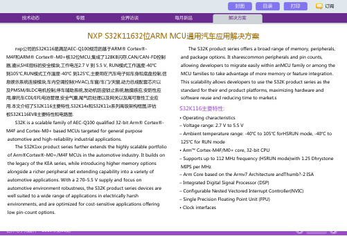
nxp公司的S32K116是满足AEC-Q100规范的基于ARM® Cortex®-M4F和ARM® Cortex®-M0+核32位MCU,集成了128KB闪存,CAN/CAN-FD控制器,遵从SHE指标的安全模块,工作电压2.7 V 到 5.5 V, RUN模式工作温度-40℃到105℃,RUN模式工作温度-40℃到125℃,主要用在汽车电子如车身和底盘控制,信息娱乐系统连接模块,车内空调控制(HVAC),车窗/车门/天窗,动力总成配套芯片以及PMSM/BLDC电机控制,停车辅助系统,发动机防盗锁止系统,触摸感应,安防性应用,摩托车CDI/EFI,电池管理,安全气囊,尾气后处理以及网关以及高可靠性工业应用.本文介绍了S32K116主要特性,S32K14x和S32K11x系列高级架构框图,评估板S32K116EVB主要特性和电路图.S32K is a scalable family of AEC-Q100 qualified 32-bit Arm® Cortex®-M4F and Cortex-M0+ based MCUs targeted for general purposeautomotive and high-reliability industrial applications.The S32K1xx product series further extends the highly scalable portfolio of Arm®Cortex®-M0+/M4F MCUs in the automotive industry. It builds on the legacy of the KEA series, while introducing higher memory optionsalongside a richer peripheral set extending capability into a variety ofautomotive applications. With a 2.70–5.5 V supply and focus onautomotive environment robustness, the S32K product series devices are well suited to a wide range of applications in electrically harshenvironments, and are optimized for cost-sensitive applications offeringlow pin-count options.The S32K product series offers a broad range of memory, peripherals, and package options. It sharescommon peripherals and pin counts,allowing developers to migrate easily within anMCU family or among the MCU families to take advantage of more memory or feature integration. This scalability allows developers to use the S32K product series as the standard for their end product platforms, maximizing hardware andsoftware reuse and reducing time to market.sS32K116主要特性:• Operating characteristics– Voltage range: 2.7 V to 5.5 V– Ambient temperature range: -40℃ to 105℃ forHSRUN mode, -40℃ to 125℃ for RUN mode• Arm™ Cortex-M4F/M0+ core, 32-bit CPU– Supports up to 112 MHz frequency (HSRUN mode)with 1.25 Dhrystone MIPS per MHz– Arm Core based on the Armv7 Architecture andThumb?-2 ISA– Integrated Digital Signal Processor (DSP)– Configurable Nested Vectored Interrupt Controller(NVIC)– Single Precision Floating Point Unit (FPU)• Clock interfacesNXP S32K11632位ARM MCU通用汽车应用解决方案– 4 - 40 MHz fast external oscillator (SOSC) with upto 50 MHz DC external square input clock inexternal clock mode– 48 MHz Fast Internal RC oscillator (FIRC)– 8 MHz Slow Internal RC oscillator (SIRC)– 128 kHz Low Power Oscillator (LPO)– Up to 112 MHz (HSRUN) System Phased LockLoop (SPLL)– Up to 20 MHz TCLK and 25 MHz SWD_CLK– 32 kHz Real Time Counter external clock(RTC_CLKIN)• Power management– Low-power Arm Cortex-M4F/M0+ core withexcellent energy efficiency– Power Management Controller (PMC) with multiplepower modes: HSRUN, RUN, STOP, VLPR, andVLPS. Note: CSEc (Security) or EEPROM writes/erase will trigger error flags in HSRUN mode (112MHz) because this use case is not allowed toexecute simultaneously.The device will need toswitch to RUN mode (80 Mhz) to execute CSEc(Security) or EEPROM writes/erase.– Clock gating and low power operation supported onspecific peripherals.• Memory and memory interfaces– Up to 2 MB program flash memory with ECC– 64 KB FlexNVM for data flash memory with ECCand EEPROM emulation. – Up to 256 KB SRAM with ECC– Up to 4 KB of FlexRAM for use as SRAM orEEPROM emulation Note: CSEc (Security) orEEPROM writes/erase will trigger error flagsinHSRUN mode (112 MHz) because this use case isnot allowed to execute simultaneously. The devicewill need to switch to RUN mode (80 MHz)toexecute CSEc (Security) or EEPROM writes/erase.– Up to 4 KB Code cache to minimize performanceimpact of memory access latencies– QuadSPI with HyperBus™ support• Mixed-signal analog– Up to two 12-bit Analog-to-Digital Converter(ADC) with up to 32 channel analog inputs permodule– One Analog Comparator (CMP) with internal 8-bitDigital to AnalogConverter (DAC)• Debug functionality– Serial Wire JTAG Debug Port (SWJ-DP) combines– Debug Watchpoint and Trace (DWT)– Instrumentation Trace Macrocell (ITM)– Test Port Interface Unit (TPIU)– Flash Patch and Breakpoint (FPB) Unit• Human-machine interface (HMI)– Up to 156 GPIO pins with interrupt functionality– Non-Maskable Interrupt (NMI)• Communications interfaces– Up to three Low Power Universal Asynchronous Receiver/Transmitter(LPUART/LIN) modules with DMA supportand low power availability– Up to three Low Power Serial Peripheral Interface (LPSPI) modules with DMA support and low power availability– Up to two Low Power Inter-Integrated Circuit (LPI2C) modules with DMA support and low power availability– Up to three FlexCAN modules (with optional CAN-FD support)– FlexIO module for emulation of communication protocols and peripherals (UART, I2C, SPI, I2S, LIN, PWM, etc).– Up to one 10/100Mbps Ethernet with IEEE1588 support and twoSynchronous Audio Interface (SAI) modules.• Safety and Security– Cryptographic Services Engine (CSEc) implements a comprehensive set of cryptographic functions as described in theSHE (Secure HardwareExtension) Functional Specification. Note: CSEc (Security) or EEPROMwrites/erase willtrigger error flags in HSRUN mode (112 MHz) because this use case is not allowed to execute simultaneously.Thedevice will need to switch to RUN mode (80 MHz) to execute CSEc(Security) or EEPROM writes/erase.– 128-bit Unique Identification (ID) number– Error-Correcting Code (ECC) on flash and SRAM memories– System Memory Protection Unit (System MPU)– Cyclic Redundancy Check (CRC) module– Internal watchdog (WDOG)– External Watchdog monitor (EWM) module• Timing and control– Up to eight independent 16-bit FlexTimers (FTM) modules, offering up to 64 standard channels (IC/OC/PWM)– One 16-bit Low Power Timer (LPTMR) with flexible wake up control– Two Programmable Delay Blocks (PDB) with flexible trigger system– One 32-bit Low Power Interrupt Timer (LPIT) with 4 channels– 32-bit Real Time Counter (RTC)• Package– 32-pin QFN, 48-pin LQFP, 64-pin LQFP, 100-pin LQFP, 100-pin MAPBGA, 144-pin LQFP, 176-pin LQFP packageoptions• 16 channel DMA with up to 63 request sources usingDMAMUXapplications, which include but not limited to:• Exterior and interior lighting• HVAC• Door/Window/Wiper/Seat controller• BLDC/PMSM motor control• Park assistant• E-shifter• TPMS• Real time control in infotainment system• Battery management system• Human machine interface such as touch sense control • Secured vehicle data transfer• Safety controller• Over the air update图1:S32K14x系列高级架构框图图2:S32K11x系列高级架构框图。
Silabs EFM32HG322 32位USB MCU开发方案
Silabs EFM32HG322 32位USB MCU开发方案
佚名
【期刊名称】《世界电子元器件》
【年(卷),期】2015(000)005
【摘要】<正>EFM32 MCU是节能型的微控制器。
EFM32H微控制器采用功能强大的32位ARM CortexM0+内核和创新型低功耗技术,从节能模式唤醒所需的时间更短,提供多种外设选择,特别适于电池供电应用以及其他需要高性能和低能耗的系统。
本文简要介绍了各个模块和EFM32HG32器件的配置。
EFM32HG322的主要特性?ARMCortex-M0+CPU平台?频率高达25 MHz的高性能32位处理器?唤醒中断控制器?灵活的能量管理系统?20n A@3V关断模式【总页数】3页(P12-14)
【正文语种】中文
【中图分类】TP332.3
【相关文献】
1.Cypress MB9B520M 32位ARM MCU开发方案 [J],
2.ST STM32L562QE超低功耗32位ARM MCU开发方案 [J],
3.NXP LPC55S16 32位ARM MCU嵌入应用开发方案 [J],
4.ST STM32L072CZ超低功耗32位ARM MCU开发方案 [J],
5.Microchip推出全新32位PIC32 MCU系列,具备以太网、CAN、USB和128 KB RAM,通过高性能连接扩展32位单片机产品组合 [J],
因版权原因,仅展示原文概要,查看原文内容请购买。
NXPS32K632位ARMMCU通用汽车应用解决方案

NXPS32K632位ARMMCU通用汽车应用解决方案NXPS32K632是一款面向汽车领域的ARM MCU通用解决方案。
随着汽车电子技术的迅猛发展和对安全性能要求的提高,高性能、低功耗、可靠性强的MCU成为了汽车行业的关注焦点。
NXPS32K632作为通用汽车应用解决方案,满足了汽车行业对MCU的高要求,实现了安全性、可靠性和可扩展性的最佳平衡。
一、高性能NXPS32K632搭载了ARM Cortex-M4内核,拥有高达100 MHz的主频。
相比较传统的8位或16位MCU,它具备了更强的计算处理能力和更高的响应速度,能够满足复杂计算和实时响应的要求。
二、低功耗在节能环保的理念下,NXPS32K632采用了低功耗制造工艺,优化了能耗管理机制。
通过控制器设计的创新和智能电源管理单元的引入,NXPS32K632实现了低功耗运行。
在传感器和电机控制等常见的汽车应用场景中,能够大幅度降低功耗,延长电池使用寿命。
三、安全性在汽车行业,安全性至关重要。
NXPS32K632提供了多层次的安全保障机制。
例如,硬件加密模块能够对数据进行加密和解密处理,防止数据泄露和篡改。
此外,NXPS32K632还支持可信硬件模块(TPM),用于存储和管理加密密钥和证书等安全数据,确保应用的安全运行。
四、可靠性作为一款面向汽车领域的MCU解决方案,NXPS32K632通过了严格的汽车行业标准和可靠性测试。
它具备良好的抗干扰能力,能够适应恶劣的工作环境。
同时,可靠的软件开发和完善的硬件设计,保证了系统的高可靠性和稳定性。
五、可扩展性NXPS32K632提供了丰富的外设接口和灵活的扩展能力,能够满足不同应用的需求。
它支持多种通信接口,例如CAN、SPI、I2C和UART等,支持外部存储器和外围设备的连接。
这为汽车电子系统的功能扩展和升级提供了便利。
综上所述,NXPS32K632作为一款ARM MCU通用汽车应用解决方案,具备高性能、低功耗、安全可靠和可扩展性等优势。
Silabs EFM32HG322F64 32位ARM MCU开发方案

Silabs EFM32HG322F64 32位ARM MCU开发方案Silabs公司的EFM32HG322F64是基于32位ARM Cortex-M0+核的低功耗微控制器,工作频率高达25MHz,采用创新的低能耗技术,短叫醒时间,以及各种外设,非常适合用在以电池为能源的应用和高性能低功耗的系统.本文介绍了EFM32HG322F64主要特性,框图,以及入门套件EFM32HG-SLSTK3400A主要特性和电路图.The EFM32 MCUs are the world’s most energy friendly microcontrollers. With a unique combinationof the powerful 32-bit ARM Cortex-M0+, innovative low energy techniques, short wake-up time fromenergy saving modes, and a wide selection of peripherals, the EFM32HG microcontroller is well suitedfor any battery operated application as well as other systems requiring high performance and low-energyconsumption. This section gives a short introduction to each of the modules in general terms and alsoshows a summary of the configuration for the EFM32HG322 devices. For a complete feature set andin-depth information on the modules, the reader is referred to the EFM32HG Reference Manual.EFM32HG322F64主要特性:• ARM Cortex-M0+ CPU platform• Hig h Performance 32-bit processor @ up to 25 MHz• Wake-up Interrupt Controller• Flexible Energy Management System• 20 nA @ 3 V Shutoff Mode• 0.6 μA @ 3 V Stop Mode, including Power-on Reset, Brown-outDetector, RAM and CPU retention• 0.9 μA @ 3 V Deep Sle ep Mode, including RTC with 32.768 kHzoscillator, Power-on Reset, Brown-out Detector, RAM and CPUretention• 53 μA/MHz @ 3 V Sleep Mode• 132 μA/MHz @ 3 V Run Mode, with code executed from flash• 64/32 KB Flash• 8/8 KB RAM• 35 General Purpose I/O pins• Configurable push-pull, open-drain, pull-up/down, input filter, drivestrength• Configurable peripheral I/O locations• 16 asynchronous external interrupts• Output state retention and wake-up from Shutoff Mode• 6 Channel DMA Controller• 6 Channel Perip heral Reflex System (PRS) for autonomous inter-peripheral signaling • Hardware AES with 128-bit keys in 54 cycles• Timers/Counters• 3× 16-bit Timer/Counter• 3×3 Compare/Capture/PWM channels• Dead-Time Insertion on TIMER0• 1× 24-bit Real-Time Counter• 1× 16-bit Pulse Counter• Watchdog Timer with dedicated RC oscillator @ 50 nA• Communication interfaces• 2× Universal Synchronous/Asynchronous Receiver/Transmitter• UART/SPI/SmartCard (ISO 7816)/IrDA/I2S• Triple buffered full/half-duplex operation• L ow Energy UART• Autonomous operation with DMA in Deep SleepMode• I2C Interface with SMBus support• Address recognition in Stop Mode• Low Energy Universal Serial Bus (USB) Device• Fully USB 2.0 compliant• On-chip PHY and embedded 5V to 3.3V regulator• Crystal-free operation• Ultra low power precision analog peripherals• 12-bit 1 Msamples/s Analog to Digital Converter• 4 single ended channels/2 differential channels• On-chip temperature sensor• Current Digital to Analog Converter• Selectable curr ent range between 0.05 and 64 uA• 1× Analog Comparator• Capacitive sensing with up to 5 inputs• Supply Voltage Comparator• Ultra efficient Power-on Reset and Brown-Out Detector• Debug Interface• 2-pin Serial Wire Debug interface• Micro Trace Buffer (MTB)• Pre-Programmed USB/UART Bootloader• Temperature range -40 to 85 ºC• Single power supply 1.98 to 3.8 V• TQFP48 package• Preliminary - This datasheet revision applies to a productunder developmentEFM32HG322F64主要应用:• Energy, gas, water and sma rt metering• Health and fitness applications• Smart accessories• Alarm and security systems• Industrial and home automation图1。
PIC32MX4:多媒体开发方案

PIC32MX4:多媒体开发方案
佚名
【期刊名称】《世界电子元器件》
【年(卷),期】2011(000)003
【摘要】@@ Microchip公司的PIC32MX4系列是高性能通用和USB的32位闪存微控制器(MCU),它的MIPS32 M4K 内核是32位内核,有5级流水线,最大频率为80MHz,性能达到1.56DMIPS/MHz(Dhrystone 2.1),MCU 工作电压从2.3V~3.6V,闪存32kB 到512kB(另有12kB引导闪存),8kB到32kB SRAM,主要用在嵌入式系统如家庭娱乐、个人娱乐和家庭网络等.
【总页数】3页(P21-23)
【正文语种】中文
【相关文献】
1.云平台下的多媒体图书系统开发方案 [J], 王笑宇;张锐
2.河流梯级开发方案模糊层次综合优选问题的探讨——桑郎河梯级开发方案优选[J], 丁时至
ttice CrossLink-NX系列低功耗FPGA开发方案 [J],
4.以威尼斯档案馆时光机项目为例探讨我国工业遗产保护开发方案 [J], 田园
5.基于开源软件的工程地质数字化开发方案研究 [J], 刘聪元
因版权原因,仅展示原文概要,查看原文内容请购买。
stm32方案

stm32方案引言STM32是意法半导体公司推出的一系列32位单片机产品。
这些产品具有低功耗、高性能和广泛的应用领域,成功地应用于工业控制、汽车电子、消费电子等领域。
在本文档中,我们将介绍STM32方案的基本概念、特点以及应用案例。
1. STM32概述1.1 STM32的起源STM32系列单片机最早由STMicroelectronics(意法半导体)于2007年推出。
其设计灵感来自ST公司的一款32位RISC处理器——ARM Cortex-M3。
Cortex-M3采用流水线方式执行指令,具有较高的执行效率和较低的功耗,在嵌入式系统领域取得了巨大的成功。
基于Cortex-M3的设计思想,STM32系列单片机在性能和功耗之间找到了平衡。
1.2 STM32系列产品意法半导体公司根据功能和性能要求,将STM32系列单片机分为不同的系列,每个系列面向特定的应用领域。
主要的系列包括:- STM32F:面向通用应用领域,具有丰富的外设和强大的处理能力。
- STM32L:面向低功耗应用领域,具有极低的静态功耗和高能效。
- STM32H:面向高性能应用领域,具有极高的处理速度和丰富的存储器资源。
- STM32G:面向智能电网应用领域,具有更高的计算能力和抗干扰能力。
1.3 STM32的特点STM32系列单片机具有以下特点:- 32位处理器:相比8位或16位单片机,32位处理器具有更高的执行速度和更大的地址空间。
- ARM Cortex-M内核:基于ARM Cortex-M内核,具有高性能、低功耗和高可靠性。
- 丰富的外设:每个系列的STM32单片机都内置了丰富的外设,如通信接口、模拟输入输出、定时器等,能够满足不同应用的需求。
- 强大的开发生态系统:意法半导体提供了丰富的开发工具和成熟的软件库,方便开发者快速开发和调试应用。
2. 应用案例2.1 工业自动化控制STM32系列单片机在工业自动化控制中得到了广泛的应用。
六款全新32位PIC32MX5-6-7单片机(Microchip)
六款全新32位PIC32MX5/6/7单片机(Microchip)Microchip Technology Inc.(美国微芯科技公司)宣布,推出六款全新32 位PIC32MX5/6/7 单片机系列产品,以全新的更具成本效益的存储容量选项提供相同的集成以太网、CAN、USB 和串行连接外设。
此外,经过设计提升后,工作电流可以低至0.5 mA/MHz,降低了功耗;闪存可承受高达2 万次的读/写周期;而且EEPROM 仿真能力更好。
同时,通过保持通用引脚位,PIC32 产品线为设计人员实现兼顾存储容量和成本的高性能应用提供了一个无缝移植路径。
嵌入式设计人员一直在寻找既降低成本又不牺牲性能或功能的方法。
Microchip 最新的80 MHz PIC32 系列单片机系列保持了1.56 DMIPS/MHz 的最佳性能,并集成了以太网、CAN、USB 和多个串行通信通道,同时提供更具成本效益的存储容量选项,从而满足了这些需求。
具体来说,该系列提供32 KB 的RAM 和高达140 KB 的闪存。
Microchip 高性能单片机部副总裁Sumit Mitra 表示:“我们致力于在PIC32 产品线的成功基础上再推六款全新单片机。
每款单片机均采用五种不同的引脚兼容封装。
这些全新高性能、连接功能丰富的单片机为客户提供了低成本的存储容量选项,可实现扩展,并支持向其他不断增加的32 位产品线的无缝移植。
”MIPS 科技公司市场营销及业务发展副总裁Art Swift 表示:“Microchip最大限度地提高了MIPS32 M4K 内核的原始性能,同时利用其高灵活性优势创建了一个32 位单片机架构,超越了苛刻的嵌入式设计要求。
Microchip 凭借这个全新PIC32 系列的性价比及其广泛的集成外设设置,为设计人员提供了极大的价值。
”这款全新PIC32 系列的应用实例包括:通信(POS 机、网络服务器和多协议。
单片机开发方案
单片机开发方案在现代科技飞速发展的时代,单片机已经渗透到我们生活的方方面面,从智能家居设备到智能手机,从汽车电子到医疗仪器,无一不离开单片机的应用。
那么,什么是单片机?如何进行单片机开发?本文将围绕这个主题,从硬件选型、软件开发及测试等多个方面进行论述。
一、硬件选型在进行单片机开发之前,首先需要选择合适的硬件平台。
市面上常见的单片机有微芯片(Microchip)的PIC系列、意法半导体(STMicroelectronics)的STM32系列、德州仪器(Texas Instruments)的MSP430系列等。
选定单片机之后,还需考虑所需外设及接口,例如ADC模块、串口、LCD显示等。
根据项目需求以及性能要求,进行综合考量,并制定相应的硬件方案。
二、软件开发1. 编程语言选择单片机的软件开发可以使用多种编程语言进行,例如C语言、汇编语言等。
C语言是单片机开发中最常用的编程语言,具有跨平台、易于学习、开发效率高等优点,适合大部分项目需求。
对于特定需求,如对算法效率要求较高的项目,可以选择使用汇编语言进行开发。
2. 集成开发环境(IDE)为了方便开发者编写、调试和测试单片机程序,通常会选择使用集成开发环境(IDE)进行开发。
常见的IDE有Keil、IAR Embedded Workbench、Code Composer Studio等,它们提供了丰富的开发工具和调试功能,同时也支持代码编辑、编译、仿真等操作,大大简化了开发流程。
3. 编程调试在进行单片机软件开发时,调试是不可或缺的一部分。
通常,开发者会使用仿真器或调试器与目标硬件连接,以便进行程序的运行、调试和测试。
这些工具不仅可以监视和修改存储在单片机中的程序,还可以查看寄存器的状态、读取和编写内存等操作,有助于解决程序中的错误。
三、测试与验证完成单片机开发后,还需要进行测试和验证,以确保程序的正确性和稳定性。
常见的测试方法包括黑盒测试和白盒测试。
ST STM32L072xx超低功耗32位ARM MCU开发方案
STM32L072x8 STM32L072xB STM32L072xZ超低功耗32位MCU基于ARM的Cortex-M0+,高达192KB闪存,20KB SRAM,6KB EEPROM,USB,ADC,DAC。
超低功耗STM32L072xx提供9种不同的封装类型,从32引脚到100引脚。
根据所选择的器件,包括不同的外设集合,以下描述概述了该系列中提出的完整系列外设。
STM32L072xx微控制器应用•燃气/水表和工业传感器•医疗保健和健身器材•远程控制和用户界面•PC外设、游戏、GPS设备•报警系统,有线和无线传感器,视频对讲STM32L072xx系列主要特性•超低功耗平台1.65V~3.6V电源-40℃~125℃温度范围0.29μA待机模式(3个唤醒引脚)0.43μA停止模式(16条唤醒线)0.86μA停止模式+RTC+20KB RAM保持时间在运行模式下降至93μA/MHz5μs唤醒时间(来自闪存)41μA12位ADC转换,速率为10ksps•内核:ARM 32位Cortex-M0+和MPU从32kHz~32MHz最大0.95 DMIPS/MHz•复位和供应管理图1 STM32L072x系列框图ST STM32L072xx超低功耗32位ARM MCU开发方案超低功耗POR/PDR可编程电压检测器(PVD)•时钟源1到25MHz晶体振荡器用于带校准的RTC的32kHz振荡器高速内部16MHz工厂校准RC(+/-1%)内部低功耗37kHz RC内部多电源低功耗65kHz~4.2MHz RC用于USB的48MHz RC的内部自校准CPU时钟PLL•预编程引导程序:USB,USART支持•发展支持:支持串行线调试•最多84个快速I/O(78个I/O,5V耐压)•存储器高达192KB带ECC的闪存(2个组具有读写同步功能)20KB RAM6KB带ECC的数据EEPROM20字节备份寄存器对R/W操作的扇区保护•丰富模拟外设12位ADC 1.14Msps,最多16个通道(降至1.65V)2个带输出缓冲器的12位通道DAC(低至1.8V)2个超低功耗比较器(窗口模式和唤醒功能,低至1.65V)•最多24个电容式感应通道支持触摸键,线性和旋转触摸传感器•7通道DMA控制器,支持ADC,SPI,I2C,USART,DAC,定时器图2 STM32L072x系列时钟树•11个外围通信接口1个USB 2.0无晶体,电池充电检测和LPM4×USART (2个采用ISO 7816,IrDA ),1×UART (低功耗)高达6×SPI 16Mbits/s 3×I 2C (2与SMBus/PMBus)•11个定时器:2×16位,最多4个通道,2×16位,最多2个通道,1×16位超低功耗定时器,1×SysTick,1×RTC ,2×16位基本DAC 和2×看门狗(独立/窗口)•CRC计算单元,96位唯一ID •真RNG 和防火墙保护图3 P-NUCLEO-LRWAN1 Nucleo包外形图Nucleo包P-NUCLEO-LRWAN1(NUCLEO-L073RZ板和I-NUCLEO-SX1272D RF扩展板)超低功耗STM32和LoRa Nucleo组件(P-NUCLEO-LRWAN1)是基于NUCLEO-L073RZ板,Semtech公司的I-NUCLEO-SX1272DLoRa RF扩展板和低于千兆赫天线。
Keil NXP LPC1114 ARM Cortex-M0 32位MCU开发方案
Keil NXP LPC1114 ARM Cortex-M0 32位MCU开发方案公司的MCB1000评估板能用来评估基于公司的 -M0和 Cortex-M3器件如NXP LPC11xx 和NXP LPC13xx系列,具有串行接口,CAN接口和 2.0全速接口以及Cortex下载和调试,而NXP公司的LPC1110/11/12/13/14/15是基于ARM 低成本的32位,CPU工作频率高达50MHz,可用于8/16位MCU的应用如计表,照明,告警系统工程和白色家电。
本文介绍了LPC1110/11/12/13/14/15主要特性和优势,方框图以及Keil MCB1000评估板主要特性和技术数据,方框图与。
The LPC1110/11/12/13/14/15 are a ARM Cortex-M0 based, low-cost 32-bit MCU family, designed for 8/16-bit microcontrollerapplications, offering performance, low power, simpleinstruction set and memory addressing together with reduced code size compared to existing 8/16-bit architectures. The LPC1110/11/12/13/14/15 operates at CPU frequencies of up to 50 MHz.The peripheral complement of the LPC1110/11/12/13/14/15 includes up to 64 kB of flash memory, up to 8 kB of data memory, one Fast-mode Plus I2C-bus interface, one RS-485/EIA-485 UART, up to two SPI interfaces with SSP features, four general purpose counter/timers, a 10-bit , and up to 42 general purpose I/O pins. LPC1110/11/12/13/14/15主要特性和优势:System:ARM Cortex-M0 processor, running at frequencies of up to 50 MHz. ARM Cortex-M0 built-in Nested Vectored Interrupt Controller (NVIC).Non-Maskable Interrupt (NMI) input selectable from several input sources (LPC1100XL series only).Serial Wire Debug.System tick timer.Memory:64 kB (LPC1115), 56 kB (LPC1114/333), 48 kB (LPC1114/323), 32 kB(LPC1114/102/201/202/203/301/302/303), 24 kB (LPC1113), 16 kB (LPC1112),8 kB (LPC1111),or 4 kB (LPC1110) on-chip flash programming memory.256 byte page erase function (LPC1100XL series only)8 kB, 4 kB, 2 kB, or 1 kB SRAM.In-System Programming (ISP) and In-Application Programming (IAP) via on-chip bootloader software.Digital peripherals:Up to 42 General Purpose I/O (GPIO) pins with configurable pull-up/pull-down resistors. In addition, a configurable open-drain mode is supported on theLPC1100L and LPC1100XL series.GPIO pins can be used as edge and level sensitive interrupt sources.High-current output driver (20 mA) on one pin.High-current sink drivers (20 mA) on two I2C-bus pins in Fast-mode Plus (not on LPC1112FDH20/102).Four general purpose counter/timers with up to eight capture inputs and up to 13 match outputs.Programmable WatchDog Timer (WDT) the LPC1100 series only. Programmable windowed WDT on the LPC1100L and LPC1100XL series only.Analog peripherals:10-bit ADC with input multiplexing among 5, 6, or 8 pinsdepending on package size.Serial interfaces:UART with fractional baud rate generation, internal FIFO, and RS-485 support.Two SPI controllers with SSP features and with FIFO andmulti-protocol capabilities (second SPI on LPC1100 and LPC1100L series LQFP48 package only).I2C-bus interface supporting full I2C-bus specification and Fast-mode Plus with a data rate of 1 Mbit/s with multiple address recognition and monitor mode (not on LPC1112FDH20/102).Clock generation:12 MHz internal RC oscillator trimmed to 1 % accuracy that can optionally be used as a system clock.Crystal oscillator with an operating range of 1 MHz to 25 MHz. Programmable watchdog oscillator with a frequency range of 7.8 kHz to 1.8 MHz.PLL allows CPU operation up to the maximum CPU rate without the need for a high-frequency crystal. May be run from the system oscillator or the internal RC oscillator.Clock output function with divider that can reflect the system oscillator clock, IRC clock, CPU clock, and the Watchdog clock. Power control:Integrated PMU (Power Management Unit) to minimize power consumption during Sleep, Deep-sleep, and Deep power-down modes. Power profiles residing in boot ROM allowing to optimize performance and minimize power consumption for any given application through one simple function call. (LPC1100Land LPC1100XL series only.)Three reduced power modes: Sleep, Deep-sleep, and Deep power-down. Processor wake-up from Deep-sleep mode via a dedicated start logic using up to 13 of the functional pins.Power-On Reset (POR).Brownout detect with four separate thresholds for interrupt and forced reset.Unique device serial number for identification.Single power supply (1.8 V to 3.6 V).Available as LQFP48 package and HVQFN33 package.LPC1100L series available as TSSOP28 package, DIP28 package, TSSOP20 package, and SO20 package.LPC1110/11/12/13/14/15应用:eMeteringLighting Alarm systems White goods。
- 1、下载文档前请自行甄别文档内容的完整性,平台不提供额外的编辑、内容补充、找答案等附加服务。
- 2、"仅部分预览"的文档,不可在线预览部分如存在完整性等问题,可反馈申请退款(可完整预览的文档不适用该条件!)。
- 3、如文档侵犯您的权益,请联系客服反馈,我们会尽快为您处理(人工客服工作时间:9:00-18:30)。
一
条件传送指令 ( MOVN,MO VZ )
向 量 中 断
一
-
硬件 实时时钟 和 日历 ( R T CC) 5个 1 6位定时器 , 计数 器 ( 两个 1 6 位结合 , 以创建两个3 2 位定时器)
一
可编 程 异 常 向 量 基 原子中断开启 , 关 闭
板相 同, 并 与众 多 A r d u i n o护 罩 兼 容 。 它具 有 一 个 U SB 串 行 端 口 接 口 , 用
一
故障保护 时钟 监视器模式
片卜 T 编 程 看 门 狗 定 时 器具
一
多达 4通道 的 D MA硬件具 有 自动
数 据 量 检 测
一
-
一
世 界电子元器件 2 0 1 4 . 2 g e c e c c n c o m
;
三 囹留脚 姐降
脂墩 0 ] 上 l > I d I L } 。∞ 匦
-
-
性能 ( 在 0等 待 状 态 闪存 访 问 )
一
周 期 乘 法 和 高性 能 除 法 单 元 MI P S1 6 e @ 模 式 , 用 于 最 多 缩小
4 0 %的代码尺 寸
图1 PI C 3 2 MX3 X X / 4 XX 系 列框 图
-
一
两组 3 2核 寄 存 器 文 件 ( 3 2位 ) ,
以 减 少 中 断 延 迟
-
预取缓存模块,以加快 存执行速度
斤 机 特 性
・
一
I : 作温度范围 一 4 0 。 C~ + 1 0 5 。 C
一
2 . 3 V ~ 3 . 6 V 【作 电 压 范 围
一
3 2 k - 5 1 2 k闪存 ( 另加 1 2 k B的闪存
启动)
-
8 k到 3 2 k的 S R AM 存储 器
一
与 大 多数 P I C 2 4 / d s PI C D S C 器 件
图2 MI P S3 2 M4 K 处 理器内核框图
-
引脚兼容
一
低功 耗 R C振荡器 以便可靠地工 作
一
U S B 2 . 0兼容 全速 没备和 On — T h e - Go的 ( OT G)控制器
一
乘 加 和 乘 减 指 令
目标 乘 法 指 令 0 / 1检 测 说 明
c h i p KI T U C3 2 7 f /  ̄ , T f
-
发 平 台
c h i p KI T U C3 2是 基 于 Ar d u i n o
最多两个 S P I 模 块
一
一
并 行主,仆端 口 ( P MP / P S P ) ,具
一
5个外部 中断引脚
高速 I , O 引脚 可 以切 换 高 达 8 0 MH z
・ MI P S 1 6 e代 码 压 缩
一
-
3 2位 指 令 的 1 6位 编 码 ,可 提 高 代 码 密 度
制 器具有 3 2位 MI P S 处理 器 内 核 ,在 8 0 MH z运 行 ,5 1 2 k的 闪 存 程 序 存 储 器和 S R A M 3 2 k数 据 存 储 器 。 UC3 2可 以 使 用 多 平 台 集 成 开
一
一
一
GP R 影 子 寄 存 器 , 以尽 量 减 少 中断 于 连 接 到 I DE, 可 以 通 过 US B 或 外
延迟
一
5个 捕 捉 输 入 5个 比较 / P WM 输 出
-
接 电源供 电。
・
位域 操 作 指 令
U C 3 2 板 采 用 功 能 强 大 的
PI C 3 2 MX 3 4 0 F 5 1 2微 控 制 器 。该 微 控
多种电源管理模式
有 独 立 的 可 编 程 优 先 级 的 多个 中断
向 量
一
・
外 设 特 性
一
一
原 子 集 ,选 择 外 设 寄 存 器 CL E A R 和 反 转 操 作
一
U S B有 一个 专 用 D MA 通 道 3 MH z  ̄ 2 5 MH z晶 体 振 荡 器 内部 8 MH z和 3 2 k H z的 振 荡 器 独立 的 P L L ,用f C P U和 U S B时 钟
多任 务嵌入控制 和高性能 音频 等。
P| c3 2 MX3 X x / 4 Xx系 歹 I j 主要 特 性
・
高性能 3 2位 RI S C CP U
.
MI P S 3 2 M4 K 3 2 一 b i t 核 与 5级 管 道 8 0 MHz的 最 高 频 率
1 . 5 Biblioteka DMI PS , MHz ( Dh r y s t o n e 2 1 )
能,集成 了 5 1 2 k B闪存和 1 2 8 k B高 速S R AM,1 0 0 MH z内部总线和缓存 ,
丁 作 温 度 40。 C - 1 0 5 。 C, 工 作 电 压2 . 3 V - 3 . 6 V,丰 要 用 在 高性 能 图 像 ,
用厂 1 接 口、 以太湖 , U S B / C A N连 接 、
有8 - b i t 和 1 6 - b _ l 数 据 和 多达 1 6个
地 址 线
-
等 待 指 令
开 源 硬 件 原 型 平 台 , 并 增 加 了
Mi c r o c h i p P I C3 2微 控 制 器 的 性 能 。 该 UC3 2的 外 形 尺 寸 与 Ar d u i n o欧 诺
一 …
‘ 一‘
。
…… 。 。 ~
\ /
.
P I C 3 2 MX 3 X X : 3 2 位M C U 开发方案
Mi c r o c h i p公 司 的 P I C3 2 MX 系
列 产 品 采 用 5级 流 水 线 MI P S 3 2 M4 K 3 2位 内 核 ,具 有 1 . 6 5 D MI P S , MH z性
L … 一 … …
一
两个 I C模 块 两个 U AR T模 块 R S ・ 2 3 2 、RS - 4 8 5和 L I N 支持 I r D A与片 上的硬 件编 码器 和解 码器
一
・ 3 2位 地 址 和 数 据 路 径
・
一
电 脑 追 踪 与 跟 踪 压 缩
-
增强的 MI P S 3 2体系结构 ( 第 2版)