AA2214SURSK, 规格书,Datasheet 资料
DFLS220L-7;中文规格书,Datasheet资料

2.0A SURFACE MOUNT SCHOTTKY BARRIER RECTIFIERPowerDI ®123Features• Guard Ring Die Construction for Transient Protection • Low Power Loss, High Efficiency• Patented Interlocking Clip Design for High Surge Current Capacity• High Current Capability and Low Forward Voltage Drop • Lead Free Finish, RoHS Compliant (Note 5) •"Green" Molding Compound (No Br, Sb)Mechanical Data• Case: PowerDI ®123 • Plastic Material: Molded Plastic, "Green" Molding Compound.UL Flammability Classification Rating 94V-0 • Moisture Sensitivity: Level 1 per J-STD-020D • Terminal Connections: Cathode Band • Terminals: Finish – Matte Tin Annealed Over Copper leadframe. Solderable per MIL-STD-202, Method 208 • Marking Information: See Page 2 • Ordering Information: See Page 2 • Weight: 0.01 grams (approximate)Maximum Ratings @T A = 25°C unless otherwise specifiedSingle phase, half wave, 60Hz, resistive or inductive load. For capacitance load, derate current by 20%.CharacteristicSymbol Value Unit Peak Repetitive Reverse Voltage Working Peak Reverse Voltage DC Blocking VoltageV RRM V RWM V R 20 V RMS Reverse Voltage V R(RMS) 14 V Average Forward CurrentI F(AV) 2.0 A Non-Repetitive Peak Forward Surge Current 8.3ms Single Half Sine-Wave Superimposed on Rated Load I FSM40AThermal CharacteristicsCharacteristicSymbol Value UnitPower Dissipation (Note 1) P D 1.67 W Power Dissipation (Note 2)P D 556 mW Thermal Resistance Junction to Ambient (Note 1) R θJA 60 °C/W Thermal Resistance Junction to Ambient (Note 2) R θJA 180 °C/W Thermal Resistance Junction to Soldering (Note 3) R θJS 10 °C/W Operating Temperature Range T J -55 to +125 °C Storage Temperature Range T STG-55 to +150 °CElectrical Characteristics @T A = 25°C unless otherwise specifiedCharacteristicSymbol Min Typ Max UnitTest ConditionReverse Breakdown Voltage (Note 4) V (BR)R 20 ⎯ ⎯ V I R = 1.0mA Forward VoltageV F ⎯ ⎯ 0.32 0.375 0.36 0.42 V I F = 1.0A I F = 2.0ALeakage Current (Note 4) I R ⎯ ⎯ 0.26 ⎯ ⎯ 1.0 mA V R = 5V, T A = 25°C V R = 20V, T A = 25°C Total CapacitanceC T ⎯ 75⎯pF V R = 10V, f = 1.0MHzNotes:1. Part mounted on 50.8mm X 50.8mm GETEK board with 25.4mm X 25.4mm copper pad, 25% anode, 75% cathode. T A = 25°C.2. Part mounted on FR-4 board with 1.8mm X 2.5mm cathode and 1.8mm X 1.2mm anode, 1 oz. copper pads. T A = 25°C.3. Theoretical R θJS calculated from the top center of the die straight down to the PCB/cathode tab solder junction.4. Short duration pulse test used to minimize self-heating effect.5. EU Directive 2002/95/EC (RoHS). All applicable RoHS exemptions applied, see EU Directive 2002/95/EC Annex Notes.Top ViewPlease click here to visit our online spice models database.I , I N S T A N T A N E O U S F O R W A R D C U R R E N T (A )F V , INSTANTANEOUS FORWARD VOLTAGE (V)Fig. 1 Typical Forward Characteristics FI , I N S T A N T A N E O U S R E V E R S E C U R R E N T (m A )V , INSTANTANEOUS REVERSE VOLTAGE (V)Fig. 2 Typical Reverse CharacteristicsRC , T O T A L C A P A C I T A N C E (p F )T V , DC REVERSE VOLTAGE (V)Fig. 3 Total Capacitance vs. Reverse VoltageROrdering Information (Note 6)Part Number CasePackaging DFLS220L-7 PowerDI ®1233000/Tape & ReelNotes: 6. For packaging details, go to our website at /datasheets/ap02007.pdf.Marking InformationDate Code KeyYear 2004 2005 2006 2007 2008 2009 2010 2011 2012 2013 2014 2015Code R S T U V W X Y Z A B CMonth Jan Feb Mar Apr May Jun Jul Aug Sep Oct Nov Dec Code 1 2 3 4 5 6 7 8 9 O N D F02A = Product Type Marking Code YM = Date Code MarkingY = Year (ex: T = 2006)M = Month (ex: 9 = September) F02A Y MPackage Outline DimensionsSuggested Pad LayoutIMPORTANT NOTICEDiodes Incorporated and its subsidiaries reserve the right to make modifications, enhancements, improvements, corrections or other changes without further notice to any product herein. Diodes Incorporated does not assume any liability arising out of the application or use of any product described herein; neither does it convey any license under its patent rights, nor the rights of others. The user of products in such applications shall assume all risks of such use and will agree to hold Diodes Incorporated and all the companies whose products are represented on our website, harmless against all damages.LIFE SUPPORTDiodes Incorporated products are not authorized for use as critical components in life support devices or systems without the expressed written approval of the President of Diodes Incorporated.PowerDI ®123Dim Min Max Typ A 3.50 3.90 3.70 B 2.60 3.00 2.80 C 1.63 1.93 1.78 D 0.93 1.000.98 E 0.85 1.25 1.00 H 0.150.250.20 L 0.550.750.65 L1 1.80 2.20 2.00 L2 0.95 1.251.10 All Dimensions in mmDimensionsValue (in mm)G 1.0 X1 2.2 X2 0.9 Y11.4 Y2 1.4HX1GX2Y2Y1分销商库存信息: DIODESDFLS220L-7。
2SK1522中文资料(renesas)中文数据手册「EasyDatasheet - 矽搜」

7.如果这些产品或技术受日本出口管理限制,必须是 日本政府根据许可证出口,不能导入比批准目地以外国家.
禁止任何转移或再出口违反出口管制法律和日本及/或目地国家相关规定.
8.请与瑞萨科技公司对这些材料或产品进一步详情 其中所载.
芯片中文手册,看全文,戳
V GS = ±25 V, V DS = 0 V DS = 360 V, V GS = 0 V DS = 400 V, V GS = 0 ID =1毫安,V DS = 10 V ID = 25 A, V GS = 10 V * 1
ID = 25 A, V DS = 10 V * 1 VDS = 10 V, V GS = 0, F = 1兆赫
芯片中文手册,看全文,戳
2SK1521, 2SK1522
绝对最大额定值
(Ta = 25°C)
项目
漏极至源极电压
2SK1521
2SK1522
门源电压
漏极电流
漏电流峰值
身体流失二极管反向漏电流
频道耗散
通道温度
储存温度
注:1.PW
10 µs, 占空比
1%
2.价值在T C = 25°C
符号
ID = 25 A, V GS = 10 V, RL = 1.2
IF = 50 A, V GS = 0
IF = 50 A, V GS = 0, di F/ DT = 100 A /μs的
3
—
远期转移导纳
|yfs|
22
输入电容
Ciss —
输出电容
Coss —
反向传输电容
Crss —
导通延迟时间 上升时间 关断延迟时间 下降时间 身体向前漏二极管 电压
37700;37701;37702;37703;中文规格书,Datasheet资料
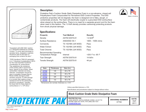
Protektive Pak’s Cushion Grade Static Dissipative Foam is a non-abrasive, closed-cell Polyethylene Foam Compounded for Permanent ESD Control Properties. The ESD protective properties will not degrade; the foam is designed not to flake, slough, or contaminate products. The foam will electrically couple to a grounded ESD worksurface when placed on the worksurface. There is no need for a separate ground cord for the foam when used in this fashion. The 1.9 lb/ft density provides cushioning protecting products from shock physical damage.
Water Extract Total Chlorine
Recommended Operating Temperature Range Internal Tear Strength Tensile Strength ASTM D3575-91 ASTM D2575-91
Item 37700 37701 37702 37703
Thickness 1/8 1/4 3/8 1/2
Size (in.) 40 x 75 40 x 75 40 x 75 40 x 75
SS14;SS16;S100;SS12;SS13;中文规格书,Datasheet资料
50 100
Figure 3. Non-Repetitive Surge Current
Figure 4. Total Capacitance
SS12-S100, Rev. C
/
TRADEMARKS
The following are registered and unregistered trademarks Fairchild Semiconductor owns or is authorized to use and is not intended to be an exhaustive list of all such trademarks.
ACEx™ Bottomless™ CoolFET™ CROSSVOLT ™ DenseTrench™ DOME™ EcoSPARK™ E2CMOSTM EnSignaTM FACT™ FACT Quiet Series™
DISCLAIMER
FAST ® FASTr™ FRFET™ GlobalOptoisolator™ GTO™ HiSeC™ ISOPLANAR™ LittleFET™ MicroFET™ MicroPak™ MICROWIRE™
SS12-S100
SS12 - S100
Features • • •
Glபைடு நூலகம்ss passivated junctions. High current capability, low VF. For use in low voltage, high frequency inverters free wheeling, and polarity protection applications.
Rev. H4
/
PSSI2021SAY,115;中文规格书,Datasheet资料
8. Application information
External resistor calculation
The output current can be set by connecting an external resistor between VS (pin 5) and REXT (pin 4).
Marking code[1] S1*
Version SOT353
PSSI2021SAY_3
Product data sheet
/
Rev. 03 — 27 August 2009
© NXP B.V. 2009. All rights reserved.
2 of 12
NXP Semiconductors
Symbol Parameter
Conditions
Min
Max Unit
Iout VS Vout VR Ptot Tstg Tj Tamb
stabilized output current supply voltage output voltage reverse voltage total power dissipation storage temperature junction temperature ambient temperature
The applied supply voltage determines the output current. Table 8 gives typical Iout values at specified supply voltages, assuming that the working output current is 70% of the maximum possible output current.
73750;73755;73760;73831;73832;中文规格书,Datasheet资料
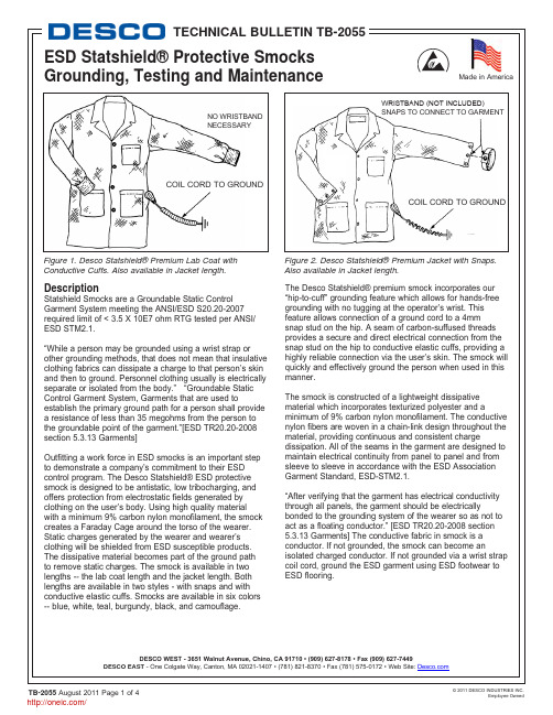
ESD Statshield® Protective Smocks Grounding, Testing and MaintenanceDescriptionStatshield Smocks are a Groundable Static Control Garment System meeting the ANSI/ESD S20.20-2007 required limit of < 3.5 X 10E7 ohm RTG tested per ANSI/ESD STM2.1.“While a person may be grounded using a wrist strap or other grounding methods, that does not mean that insulative clothing fabrics can dissipate a charge to that person’s skin and then to ground. Personnel clothing usually is electrically separate or isolated from the body.” “Groundable Static Control Garment System, Garments that are used toestablish the primary ground path for a person shall provide a resistance of less than 35 megohms from the person to the groundable point of the garment.”[ESD TR20.20-2008 section 5.3.13 Garments]Outfitting a work force in ESD smocks is an important step to demonstrate a company’s commitment to their ESD control program. The Desco Statshield® ESD protective smock is designed to be antistatic, low tribocharging, and offers protection from electrostatic fields generated by clothing on the user’s body. Using high quality material with a minimum 9% carbon nylon monofilament, the smock creates a Faraday Cage around the torso of the wearer. COIL CORD TO GROUNDMade in AmericaWRISTBAND (NOT INCLUDED)SNAPS TO CONNECT TO GARMENTCOIL CORD TO GROUNDNO WRISTBAND NECESSARYFigure 1. Desco Statshield® Premium Lab Coat with Conductive Cuffs. Also available in Jacket length.- 3651 Walnut Avenue, Chino, CA 91710 • (909) 627-8178 • Fax (909) 627-7449 - One Colgate Way, Canton, MA 02021-1407 • (781) 821-8370 • Fax (781) 575-0172 • Web Site:YES!YES!NO!NO!Figure 4. Grounding the smockFigure 6. TestersThe user and the smock will now be properly grounded. The “hip to cuff” grounding feature allows greater freedom of movement of user’s arms and hands, and a reliable path to ground while the ESD smock offers extra protection against damaging electrostatic fields which may be generated by the user’s clothing.NOTE: ANSI/ESD S20.20 REQUIRES THAT THE GROUND CORD SELECTED FOR GROUNDING OFPERSONNEL CONTAIN A BUILT-IN CURRENT LIMITING 1 MEGOHM RESISTOR.Heat Sealed PatchesIt is possible to heat seal patches to our smocks. The patch should be small and the smock should be tested before and after application.192501935019780分销商库存信息:DESCO737507375573760 738317383273833 737657383473851 738527385373854 737497377073835 736117361273613 736147365173652 736537365473855 737717361573655 736167363173635 736007360673607 736107361773618 736197362073626 736277362873629 736307363673637 736387363973640 736467364773648 736497365073657 736587365973699 737417374273743 737447377273773 738207382673827 738287382973830 738367383773838 738397384073846 738477384873849 738507385673857 73859。
VAL;VAL2;VAV;VAM;VAM-1;中文规格书,Datasheet资料
Side
No
Standard (80°C)
Solder terminals (A)
Quick-connect terminals (#187)(C2)
Quick-connect terminals (#250)(C)
Thermoplastic case
V-21
V-16
V-11
21 A
16 A
11 A
Quick-connect terminals (#187)(C2)
Quick-connect terminals (#250)(C)
Yes
Standard Solder terminals (A)
(80°C)
Quick-connect
terminals (#187)(C2)
Quick-connect terminals (#250)(C)
4. Contact Form COM Terminal, Bottom position: 1: SPDT 2: SPST-NC 3: SPST-NO
COM Terminal, Side position: 4: SPDT 5: SPST-NC
6: SPST-NO
5. Terminals A: Solder terminals C2: Quick-connect terminal (#187) C: Quick-connect terminal (#250)
■ List of Models
Thermoplastic Case
21 A (OF: 400 gf)
Thermosetting case
V-15
V-10
15 A
10 A
400 gf 200 gf 200 gf 100 gf
BSS84AKS,115;中文规格书,Datasheet资料
1.Product profile1.1General descriptionDual P-channel enhancement mode Field-Effect Transistor (FET) in a very small SOT363 (SC-88) package using Trench MOSFET technology.1.2Features and benefitsLogic-level compatible Very fast switchingTrench MOSFET technologyESD protection up to 1 kV AEC-Q101 qualified1.3ApplicationsRelay driverHigh-speed line driverHigh-side loadswitch Switching circuits1.4Quick reference data[1]Device mounted on an FR4 Printed-Circuit Board (PCB), single-sided copper, tin-plated, mounting pad for drain 1 cm 2.BSS84AKS50 V, 160 mA dual P-channel Trench MOSFETRev. 1 — 23 May 2011Product data sheetTable 1.Quick reference data Symbol ParameterConditions Min Typ Max Unit Per transistorV DS drain-source voltage T j =25°C---50V V GS gate-source voltage -20-20VI D drain currentV GS =-10V;T amb =25°C [1]---160mA Static characteristics (per transistor)R DSondrain-source on-state resistanceV GS =-10V;I D =-100mA; T j =25°C-4.57.5Ω2.Pinning information3.Ordering information4.Marking[1]% = placeholder for manufacturing site codeTable 2.Pinning information Pin Symbol Description Simplified outline Graphic symbol1S1source 1SOT363 (TSSOP6)2G1gate 13D2drain 24S2source 25G2gate 26D1drain 1132456sym147G1G2Table 3.Ordering informationType numberPackage NameDescriptionVersion BSS84AKSTSSOP6plastic surface-mounted package; 6 leadsSOT363Table 4.Marking codesType number Marking code [1]BSS84AKS%VY5.Limiting valuesTable 5.Limiting valuesIn accordance with the Absolute Maximum Rating System (IEC 60134).Symbol Parameter Conditions Min Max Unit Per transistorV DS drain-source voltage T j=25°C--50VV GS gate-source voltage-2020VI D drain current V GS=-10V; T amb=25°C[1]--160mAV GS=-10V; T amb=100°C[1]--100mA I DM peak drain current T amb=25°C; single pulse; t p≤10µs--640mA P tot total power dissipation T amb=25°C[2]-280mW[1]-320mWT sp=25°C-990mW Per deviceP tot total power dissipation T amb=25°C[2]-445mW T j junction temperature-55150°C T amb ambient temperature-55150°C T stg storage temperature-65150°C Source-drain diodeI S source current T amb=25°C[1]--160mA ESD maximum ratingV ESD electrostatic discharge voltage HBM[3]-1000V[1]Device mounted on an FR4 Printed-Circuit Board (PCB), single-sided copper, tin-plated, mounting pad for drain 1 cm2.[2]Device mounted on an FR4 Printed-Circuit Board (PCB), single-sided copper, tin-plated and standard footprint.[3]Measured between all pins.6.Thermal characteristicsTable 6.Thermal characteristicsSymbol Parameter Conditions Min Typ Max Unit Per deviceR th(j-a)thermal resistance from junction to ambient in free air[1]--300K/W Per transistorR th(j-a)thermal resistance from junction to ambient in free air[1]-390445K/W[2]-340390K/W R th(j-sp)thermal resistance from junction to solder point--130K/W[1]Device mounted on an FR4 PCB, single-sided copper, tin-plated and standard footprint.[2]Device mounted on an FR4 Printed-Circuit Board (PCB), single-sided copper, tin-plated, mounting pad for drain 1 cm2.7.CharacteristicsTable 7.CharacteristicsSymbol Parameter Conditions Min Typ Max Unit Static characteristics (per transistor)V(BR)DSS drain-source breakdownvoltageI D=-10µA; V GS=0V;T j=25°C-50--VV GSth gate-source thresholdvoltageI D=-250µA; V DS=V GS; T j=25°C-1.1-1.6-2.1VI DSS drain leakage current V DS=-50V; V GS=0V; T j=25°C---1µAV DS=-50V; V GS=0V; T j=150°C---2µA I GSS gate leakage current V GS=-20V;V DS=0V; T j=25°C---10µAV GS=20V;V DS=0V; T j=25°C---10µAR DSon drain-source on-stateresistance V GS=-10V;I D=-100mA; T j=25°C- 4.57.5ΩV GS=-10V;I D=-100mA; T j=150°C-813.5ΩV GS=-5V; I D=-100mA; T j=25°C- 5.78.5Ωg fs forward transconductance V DS=-10V; I D=-100mA; T j=25°C-150-mS Dynamic characteristics (per transistor)Q G(tot)total gate charge V DS=-25V; I D=-200mA; V GS=-5V;T j=25°C -0.260.35nCQ GS gate-source charge-0.12-nC Q GD gate-drain charge-0.09-nCC iss input capacitance V DS=-25V; f=1MHz; V GS=0V;T j=25°C -2436pFC oss output capacitance- 4.5-pF C rss reverse transfercapacitance- 1.3-pFt d(on)turn-on delay time V DS=-30V; R L=250Ω; V GS=-10V;R G(ext)=6Ω; T j=25°C -1326nst r rise time-11-ns t d(off)turn-off delay time-4896ns t f fall time-25-ns Source-drain diode (per transistor)V SD source-drain voltage I S=-115mA; V GS=0V; T j=25°C-0.48-0.85-1.2V分销商库存信息: NXPBSS84AKS,115。
M1MA141KT1G;M1MA141KT1;中文规格书,Datasheet资料
THERMAL CHARACTERISTICS
Rating Power Dissipation Junction Temperature Storage Temperature Symbol PD TJ Tstg Max 150 150 -- 55 ~ + 150 Unit mW C C
Mx M G G
Semiconductor Components Industries, LLC, 2010
October, 2010 - Rev. 7
1
Publication Order Number: M1MA141KT1/D
/
M1MA141KT1G, M1MA142KT1G
Stresses exceeding Maximum Ratings may damage the device. Maximum Ratings are stress ratings only. Functional operation above the Recommended Operating Conditions is not implied. Extended exposure to stresses above the Recommended Operating Conditions may affect device reliability. 1. t = 1 sec
3
/
M1MA141KT1G, M1MA142KT1G
PACKAGE DIMENSIONS
SC-70 (SOT-323) CASE 419--04 ISSUE N
D e1
NOTES: 1. DIMENSIONING AND TOLERANCING PER ANSI Y14.5M, 1982. 2. CONTROLLING DIMENSION: INCH. DIM A A1 A2 b c D E e e1 L HE MIN 0.80 0.00 0.30 0.10 1.80 1.15 1.20 0.20 2.00 MILLIMETERS NOM MAX 0.90 1.00 0.05 0.10 0.70 REF 0.35 0.40 0.18 0.25 2.10 2.20 1.24 1.35 1.30 1.40 0.65 BSC 0.38 0.56 2.10 2.40 MIN 0.032 0.000 0.012 0.004 0.071 0.045 0.047 0.008 0.079 INCHES NOM 0.035 0.002 0.028 REF 0.014 0.007 0.083 0.049 0.051 0.026 BSC 0.015 0.083 MAX 0.040 0.004 0.016 0.010 0.087 0.053 0.055 0.022 0.095
2026-35-C2F,2026-23-ALF,2026-26-ALF,2026-35-ALF,2026-60-ALF,2026-15-A1LF, 规格书,Datasheet 资料
*RoHS Directive 2002/95/EC Jan 27, 2003 including Annex. Specifi cations are subject to change without notice.Customers should verify actual device performance in their specifi c applications.Test Methods per ITU-T (CCITT) K.12, IEEE C62.31, RUS PE-80, Telcordia GR 1361CharacteristicModel No.2026-072026-092026-152026-202026-232026-252026-26DC Sparkover ±20 % @ 100 V/s 75 V 90 V 150 V 200 V 230 V 250 V 260V 1Impulse Sparkover 100 V/µs 1000 V/µs 275 V 700 V275 V 600 V350 V 575 V425 V 625 V450 V 650 V475 V 700 V475 V 700 VImpulse Transverse Delay .............................................1000 V/µs .................................................................< 75 ns Insulation Resistance ...................................................100 V (50 V for Model 2026–07 & 2026-09) .............> 1010 Ω Glow Voltage ................................................................10 mA .......................................................................~ 70 V Arc Voltage ...................................................................1A .............................................................................~ 10 V Glow-Arc Transition Current ...........................................................................................................................< 0.5 A Capacitance .................................................................1 MHz .......................................................................< 2 pF DC Holdover Voltage 2 .................................................>135 V , (52 V for Model 2026-07 & 2026-09, ...........< 150 ms 80 V for Model 2026-15)Impulse Discharge Current ...........................................40000 A, 8/20 µs 3 .................................................... 1 operation minimum 20000 A, 8/20 µs ......................................................> 10 operations 5000 A, 10/350 µs ................................................... 1 operation 1000 A, 10/1000 µs .................................................> 400 operationsAlternating Discharge Current ......................................130 Arms, 11 cycles 3 ............................................... 1 operation minimum 20 Arms, 1 s .............................................................> 10 operations Operation and Storage Temperature .............................................................................................................. -40 to +90 °C Climatic Category (IEC 60068-1) .................................................................................................................... 40/ 90/ 21Optional Switch-Grade Fail-short device available.Notes:• UL recognized component, UL File E153537.• Model number marking on tube: 26-xxx V .• The rated discharge current for TRIGARD ® Gas Discharge Tubes is the total current equally divided between each line to ground. • Sparkover limits after life ±25 %, IR >108Ω (-25 %,+30 % for Model 2026-07, 2026-09 and 2026-60).• Line to Line voltage is approximately 1.8 to 2 times the stated Line to Ground breakdown voltage.• At delivery AQL 0.65 Level II, DIN ISO 28591 Tube meets BT requirement Type 14 A/1 (210-310 V).2 Network applied.3 DC Sparkover may exceed ±25 % after discharge, but will continue to protect without venting.*R o H S C O M P L I A N T V E R S I O N S A V A I L A B L ECharacteristicModel No.2026-302026-352026-402026-422026-472026-60DC Sparkover ±20 % @ 100 V/s 300 V 350 V 400 V 420 V 470 V 600 V Impulse Sparkover 100 V/µs 1000 V/µs500 V 775 V625 V 875 V675 V 925 V725 V 1000 V800 V 1100 V925 V 1250 VSpecifi cations are subject to change without notice.Customers should verify actual device performance in their specifi c applications.Product Dimensions (additional lead form confi gurations available upon request)How to Order2026 - nn - x n F LFModel Number DesignatorVoltage (Divided by 10) 07 = 75 V 30 = 300 V 09 = 90 V 35 = 350 V 15 = 150 V 40 = 400 V 20 = 200 V 42 = 420 V 23 = 230 V 47 = 470 V 25 = 250 V 60 = 600 V 26 = 260 V LeadsA = None C = 1 mmLead Shape(See Product Dimension Drawings) Fail-Short OptionBlank = Standard Product F = With Fail-Short MechanismRoHS Compliant Option Blank = S tandard ProductLF = RoHS Compliant Product2026-XX-ADIMENSIONS: MILLIMETERSUNITS WITH LEADS ARE BASED ON THE2026-XX-A1 BODY .2026-XX-A12026-XX-C22026-XX-C32026-XX-C42026-XX-C82026-XX-C1.0 mm dia. lead wireFAIL-SHORT CONFIGURATION2026-XX-C2F SHOWNREV . 04/11Specifi cations are subject to change without notice.Customers should verify actual device performance in their specifi c applications.Switch-Grade Fail-short Device Shorting Curve 2026-XX-XF10.020.030.05.0C u r r e n t (A ) (E L T G S )1.00.50.1110100ELTGS = Each Line to Ground SimultaneouslyNOTE: When using a GDT fail-short device, it is imperative that all components associated and connected to the GDT with failsafe be tested in their respective completely integrated environment (finished product) to assure desired operation.Seconds1000。
- 1、下载文档前请自行甄别文档内容的完整性,平台不提供额外的编辑、内容补充、找答案等附加服务。
- 2、"仅部分预览"的文档,不可在线预览部分如存在完整性等问题,可反馈申请退款(可完整预览的文档不适用该条件!)。
- 3、如文档侵犯您的权益,请联系客服反馈,我们会尽快为您处理(人工客服工作时间:9:00-18:30)。
SPEC NO: DSAK2209 REV NO: V.2 DATE: APR/13/2011 PAGE: 1 OF 6 APPROVED: WYNEC CHECKED: Allen Liu DRAWN: J.Yu ERP: 1201005725
2.2x1.4mm SURFACE MOUNT LED LAMP Part Number: AA2214SURSK Hyper Red
Features z2.2mm x 1.4mm, 1.3mm high. zLow power consumption. zAvailable on tape and reel. zPackage : 2000pcs / reel. zMoisture sensitivity level : level 3. zRoHS compliant. Description The Hyper Red source color devices are made with Al-GaInP on GaAs substrate Light Emitting Diode.
Package Dimensions
Notes: 1. All dimensions are in millimeters (inches). 2. Tolerance is ±0.2(0.008") unless otherwise noted. 3. The specifications, characteristics and technical data described in the datasheet are subject to change without prior notice. 4. The device has a single mounting surface. The device must be mounted according to the specifications.
芯天下--http://oneic.com/SPEC NO: DSAK2209 REV NO: V.2 DATE: APR/13/2011 PAGE: 2 OF 6 APPROVED: WYNEC CHECKED: Allen Liu DRAWN: J.Yu ERP: 1201005725
Handling Precautions Compare to epoxy encapsulant that is hard and brittle, silicone is softer and flexible. Although its characteristic significantly reduces thermal stress, it is more susceptible to damage by external mechanical force. As a result, special handling precautions need to be observed during assembly using silicone encapsulated LED products. Failure to comply might lead to damage and premature failure of the LED.
1. Handle the component along the side surfaces by using forceps or appropriate tools.
2. Do not directly touch or handle the silicone lens surface. It may damage the internal circuitry. 3. Do not stack together assembled PCBs containing exposed LEDs. Impact may scratch the silicone lens or damage the internal circuitry.
4.1. The outer diameter of the SMD pickup nozzle should not exceed the size of the LED to prevent air leaks. The inner diame-ter of the nozzle should be as large as possible. 4.2. A pliable material is suggested for the nozzle tip to avoid scratching or damaging the LED surface during pickup. 4.3. The dimensions of the component must be accurately programmed in the pick-and-place machine to insure precise pickup and avoid damage during production.
5. As silicone encapsulation is permeable to gases, some corrosive substances such as H2S might corrode silver plating of
leadframe. Special care should be taken if an LED with silicone encapsulation is to be used near such substances.
芯天下--http://oneic.com/SPEC NO: DSAK2209 REV NO: V.2 DATE: APR/13/2011 PAGE: 3 OF 6 APPROVED: WYNEC CHECKED: Allen Liu DRAWN: J.Yu ERP: 1201005725
Selection Guide Notes: 1. θ1/2 is the angle from optical centerline where the luminous intensity is 1/2 of the optical peak value. 2. Luminous intensity/ luminous Flux: +/-15%.
Absolute Maximum Ratings at TA=25°C Electrical / Optical Characteristics at TA=25°C Notes: 1.Wavelength: +/-1nm. 2. Forward Voltage: +/-0.1V.
Note: 1. 1/10 Duty Cycle, 0.1ms Pulse Width.
Part No. Dice Lens Type Viewing Angle [1] Min. Typ. 2θ1/2 AA2214SURSK Hyper Red (AlGaInP) Water Clear 180 350 120° Iv (mcd) [2] @ 20mA
Symbol Parameter Device Typ. Max. Units Test Conditions λpeak Peak Wavelength Hyper Red 650 nm IF=20mA λD [1] Dominant Wavelength Hyper Red 630 nm IF=20mA Δλ1/2 Spectral Line Half-width Hyper Red 28 nm IF=20mA C Capacitance Hyper Red 35 pF VF=0V;f=1MHz VF [2] Forward Voltage Hyper Red 1.95 2.5 V IF=20mA IR Reverse Current Hyper Red 10 uA VR=5V
Parameter Hyper Red Units Power dissipation 75 mW DC Forward Current 30 mA Peak Forward Current [1] 185 mA Reverse Voltage 5 V Operating Temperature -40°C To +85°C Storage Temperature -40°C To +85°C
芯天下--http://oneic.com/SPEC NO: DSAK2209 REV NO: V.2 DATE: APR/13/2011 PAGE: 4 OF 6 APPROVED: WYNEC CHECKED: Allen Liu DRAWN: J.Yu ERP: 1201005725
Hyper Red AA2214SURSK 芯天下--http://oneic.com/SPEC NO: DSAK2209 REV NO: V.2 DATE: APR/13/2011 PAGE: 5 OF 6 APPROVED: WYNEC CHECKED: Allen Liu DRAWN: J.Yu ERP: 1201005725
AA2214SURSK Reflow soldering is recommended and the soldering profile is shown below. Other soldering methods are not recommended as they might cause damage to the product.
Recommended Soldering Pattern (Units : mm; Tolerance: ± 0.1) Reel Dimension Tape Dimensions (Units : mm)
芯天下--http://oneic.com/