freescale单片机SPI通信
freescale MC9S12P128中文手册

1Chapter1 Device Overview MC9S12P-Family 1.1介绍The MC9S12P 系列单片机是经过优化后有着低成本、高性能、低引脚数的汽车专业级单片机产品,该产品倾向于弥补高端16位单片及产品如MC9S12XS和低端8位单片机产品之间的空缺。
MC9S12P 主要针对于要求使用CAN 或者LIN/J2602通讯接口的汽车应用产品,典型的应用案例包括车身控制器、乘坐人员检测、车门控制、座椅控制、遥控车门开关信号接收器、智能执行器、车灯模块、智能接线器。
The MC9S12P 系列单片机使用了很多MC9S12XS系列单片机相同的功能,包括片内闪存错误纠正代码(ECC)、一个专为数据诊断或者数据存储的单独的数据闪存模块、高速AD转换器和高频调制锁相环(IPLL)有效改善电磁兼容性能。
MC9S12P系列单片机提供的所有16为单片机优点和微处理器效率,同时保持飞思卡尔用户熟悉的8位及16位单片机,低成本,功耗,EMC和高效的代码80针QFP、64针LQFP、40针QFN封装产品,最大限度的与MC9S12尺寸的优点,如同MC9S12XS一样可以无需等待外围设备和内存的状态既可以运行16为带款的寻址,MC9S12P系列单片机主要有XS引脚兼容. I/O口在各种模式下都可以使用,同时具有中断功能的I/O口还可以在停止或等待模式下唤醒。
1.2 芯片特性表一:提供了MC9S12P家庭成员特征摘要,1.P或D寄存器擦除或者编程需要最低总线频率为1MHZ1.2.2 芯片功能• S12 CPU 内核• 高达128 KB具有ECC功能的片上闪存• 4 Kbyte带ECC功能的数据闪存• 高达6 Kb片上静态存储器(SRAM)• 具有内部滤波器的锁相环倍频器(IPLL)• 4–16 MHz 皮尔斯振荡器• 1 MHz内部RC振荡器• 定时器(TIM) 具有16位输入捕捉、输出比较、计数器脉冲累加器功能• 具有8位6通道的脉冲调制模块(PWM)• 10通道12位分辨率的逐次逼近AD转换器• 1个串行通信外部接口(SPI)• 1个支持局域网通讯串行通信(SCI) 模块•一个多可扩展控制器区域网络(MSCAN) 模块(支持CAN 协议2.0A/B)•片上电压调节器(VREG) 可对内部供电及内部电压整流• 自主周期中断(API)1.3 模块特征1.3.1 CPUS12 CPU 是一个高速的16位处理单元:•全16-bit数据通道提供有效的数学运算和高速的数学执行• 包含很多单字节指令,可以有效的利用ROM空间• 宽域变址寻址功能:—采用堆栈指针作为所有变址操作的变址寄存器—除了在自增或自减模式下都可以利用程序计数器作为变址寄存器—使用A\B\D累加器做累加器偏移—自动变址,前递增(++a)、前递减(--a)、后递减(a--)、后递增(a++)(by –8 to +8)1.3.2 带ECC功能的片内闪存• 高达128 Kb程序闪存空间— 32 位数据加7 位ECC (纠错码) 允许单字节纠错和双字节纠错— 512字节擦出扇区空间—自动编程和擦除算法—用户设置读写页面边界—具有可以防止偶然编程或者擦除的保护结构• 4 Kb 数据闪存空间— 16 位数据加6位纠错码允许单字节和双字节纠错功能— 256 字节的擦出扇区空间—自动编程和擦除算法—用户设置读写页面边界1.3.3 片内静态存储器3高达6kb通用RAM1.3.4 外部晶振(XOSC)• 闭环控制皮尔斯晶振频率为4MHZ---16MHZ—振幅增益控制输出电流—低谐波失真信号Signal with low harmonic distortion—低功耗—良好的噪声免疫—无需外部限流电阻—跨导尺寸优化提供良好的振荡器启动保证1.3.5 内部RC晶振(IRC)• 可调的内部参考时钟—频率: 1 MHz—在–40°C to +125°C环境温度范围内调节精度达: 1.5%1.3.6 内部锁相环倍频器(IPLL)—无需外部元件—参考分频器和倍频器提供大变化量的时钟频率—自动带宽控制低频率抖动操作—自动锁定频率—可配置的选项,扩频减少电磁干扰EMC (频率调制frequency modulation) —参考时钟源:–外部4–16 MHz 共振器/晶振(XOSC)–内部RC晶振1 MHz (IRC)1.3.7 系统支撑• 上电复位(POR)• 系统复位发生器• 非法寻址复位•低电压检测中断或复位• 实时中断(RTI)• 计算机正常工作复位(COP) 开门狗—可通过相应窗口设置COP用以采用错误侦测复位通过位操作对闪存进行初始化复位•时钟监控器监控晶振功能正常工作1.3.8 定时器(TIM)• 8通道16位定时器可进行输入捕捉和输出比较• 16-bit带有7位精度预分频器的自由运行计数器•一通道16-bit 脉冲累加器1.3.9 脉冲带宽调制器(PWM)• 6通道8位or 3 通道16-bit脉宽调制器—每个通道都可以对周期和占空比进行编程—中心对齐或者左对齐输出—宽频率范围内可编程逻辑时钟1.3.10 局域网控制器(MSCAN)•速率达1Mbit/s, 满足CAN 2.0 A, B 协议—标准和扩展数据帧— 0–8 字节长度—可编程比特率达1 Mbps•5个FIFO(先进先出)的接收缓冲器•三个内部优先发送缓冲器• 灵活的标识符可编程选通滤波器s:— 2 x 32-bit— 4 x 16-bit— 8 x 8-bit•集成了低通滤波器的唤醒操作• 闭环反馈自检测• CAN 总线监听•总线关闭可通过软件干预或者自动恢复• 16-bit 接收发送信息时钟戳1.3.11 串行通信接口(SCI)•可选择全双工或单工模式•标准的不归零格式•通过可编程脉宽调制选用IrDA 1.4 反转归零格式• 13位波特率可选•可编程字符长度•可编程改变其接收和发送极性for transmitter and receiver•边沿触发接收唤醒•支持LIN总线的间隔检测和传输冲突检测1.3.12 Serial Peripheral Interface Module (SPI) •可配置8- or 16-bit 数据大小•全双工或单线双向•全双工接收和发送• Master or slave 模式•最高位优先or 最低位优先可换• 并口时钟频率相位和极性选择1.3.13 AD转换(ATD)• 10通道12位AD转换器— 3微妙转换时间— 8-/10-/12-位解决方案5—数据结果左对齐或右对齐—停止模式下使用内部晶振作为转换器晶振—低功耗模式下模拟信号比较唤醒—连续转换模式e—多通道扫描•引脚可作为IO口1.3.14 片内电压调节器(VREG)•具有带隙标准的线性电压稳压器• 具有低电压中断功能的低压检测器•上电复位(POR) 电路•低电压复位功能(LVR)•高温传感器1.3.15 背景调试(BDM)• 非插入内存访问指令• 支持在线对片内非易始性存储单元编程1.3.16 调试器(DBG)•64个入口跟踪缓冲器• 三个比较器(A, B and C)—比较器A比较全16位地址总线额16位数据总线—精确寻址和寻址范围比较•两种匹配比较类型—标记位—程序强行置位该类型是在一数学公式出现后一个指令边界可用•四个跟踪模式•四个阶段状态序列发生器stage state sequencer1.4 内部结构框图71.5 引脚图1.6 存储器映像表Table 1-2. Device Register Memory Map注意在表1-2中保留的寄存器空间不分配给任何模块,该寄存器的保留空间是留给以后使用的,对这些保留空间写操作没有任何效果,读该空间返回值都为零。
串行外设接口SPI
SPI波特率寄存器(SPI1BR)
数据位 定义 复位
D7 0 0 D6 SPPR2 0 D5 SPPR1 0 D4 SPPR0 0 D3 0 0 D2 SPR2 0 D1 SPR1 0 D0 SPR0 0
D6~D4—SPPR[2:0]为SPI波特率预分频系数 D2~D0—SPR[2:0]为SPI波特率系数源自D1SPISWAI 0
D0
SPC0 0
复位
第7、6、5和2位无效,总为0 D4—MODFEN为主模式故障功能使能 D3—BIDIROE为双向模式输出使能—双向模式由SPI管脚控制0 (SPC0=1)使能时,BIDIROE决定SPI数据输出驱动器是否被使能 为单个双向SPI I/O管脚 D1—SPISWAI为SPI停止在等待模式中 D0—SPC0为SPI管脚控制0。SPC0位用于选择单线双向模式
CPHA=0,CPOL=0时的数据/时钟时序图
CPHA=0,CPOL=1时的数据/时钟时序图
CPHA=1,CPOL=0时的数据/时钟时序图
CPHA=1,CPOL=1时的数据/时钟时序图
8.1.4
模拟SPI
对于不带SPI串行总线接口的MCU来说,可以使用软 件来模拟SPI的操作。举例说明,我们可以使用三个 普通I/O口,分别定 义为pin_SPSCK、pin_MISO、 pin_MOSI来模拟SPI器件的SPSCK、MISO、MOSI
SPI寄存器简介
偏移地址
寄存器名称与缩写
基本功能
配置SPI的基本操作模式(中断 使能、系统使能、发送中断使 能、主从模式、时钟相位、时 钟极性等) 主模式故障功能使能、双向模 式输出 为SPI主机设定预定位速率分频 因子 返回SPI的状态 读取该寄存器将返回从接收数 据缓冲器中读取的数据。写该 寄存器将会把数据写入发送数 据缓冲器
Freescale 半导体用户指南说明书
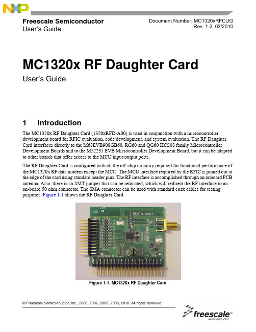
Freescale Semiconductor User’s GuideDocument Number: MC1320xRFCUGRev. 1.2, 03/20101IntroductionThe MC1320x RF Daughter Card (1320xRFD-A00) is used in conjunction with a microcontroller development board for RFIC evaluation, code development, and system evaluation. The RF Daughter Card interfaces directly to the M68EVB908GB60, RG60 and QG60 HCS08 family Microcontroller Development Boards and to the M52235 EVB Microcontroller Development Board, but it can be adapted to other boards that offer access to the MCU input/output ports.The RF Daughter Card is configured with all the off-chip circuitry required for functional performance of the MC1320x RF data modem except the MCU. The MCU interface required by the RFIC is pinned out at the edge of the card using standard header pins. The RF interface is accomplished through an onboard PCB antenna. Also, there is an SMT jumper that can be relocated, which will redirect the RF interface to an on-board 50 ohm connector. The SMA connector can be used with standard coax cables for testing purposes. Figure 1-1 shows the RF Daughter Card.Figure1-1. MC1320x RF Daughter CardMC1320x RF Daughter CardUser’s GuideIntroductionFigure1-2 shows the RF Daughter Card installed in a GB60 development board.Figure1-2. MC1320xRF Daughter Card In GB60 Development Board Figure1-3 shows the M52235 EVB development board.Figure1-3. M52235 EVB Development BoardSafety Information 2Safety InformationAny modifications to this product may violate the rules of the Federal Communications Commission and make operation of the product unlawful.47 C.F.R. Sec. 15.21This equipment has been tested and found to comply with the limits for a Class B digital device, pursuant to part 15 of the FCC Rules. These limits are designed to provide reasonable protection against harmful interference in a residential installation. This equipment generates uses and can radiate radio frequency energy and, if not installed and used in accordance with the instructions, may cause harmful interference to radio communications. However, there is no guarantee that interference will not occur in a particular installation. If this equipment does cause harmful interference to radio or television reception, which can be determined by turning the equipment off and on, the user is encouraged to try to correct the interference by one or more of the following measures:•Reorient or relocate the receiving antenna.•Increase the separation between the equipment and receiver.•Connect the equipment into an outlet on a circuit different from that to which the receiver is connected.•Consult the dealer or an experienced radio/TV technician for help.47 C.F.R. Sec.15.105(b)This equipment complies with FCC radiation exposure limits set forth for an uncontrolled environment. The antenna(s) used for this equipment must be installed to provide a separation distance of at least 8 inches (20cm) from all persons.This device complies with Part 15 of the FCC Rules. Operation is subject to the following two conditions:•This device may not cause harmful interference.•This device must accept any interference received, including interference that may cause undesired operation.3Revision HistoryThe following table summarizes revisions to this document since the previous release (Rev 1.1).Revision HistoryLocation RevisionSection 6Updated document cross reference.MC1320x MCU Interface4MC1320x MCU InterfaceFigure4-1 shows the typical connections between the MC1320x transceiver and a microcontroller unit (MCU). See the MC13202/203 Reference Manual, document MC13202RM, for interface considerations. Details about the interconnects for both the GB60 and M52235 Development boards are described in Section5.1, “Development Board Interconnects”. ArrayFigure4-1. MCU Interface PinoutDaughter Card Description 5Daughter Card DescriptionAs shown in Figure5-1 and Figure8-1, connector J101 is the main interface to the GB60 Development Board. The interface connections described in Section5.1, “Development Board Interconnects”, fall under the following three broad categories:1.Serial Peripheral Interface (SPI)2.Control3.PowerFigure1-2 shows how the RF Daughter Card is mounted on the GB60 Development Board.NOTEEnsure that zero ohm resistor R104 is in place on the MC1320x DaughterCard. As of this release, previous versions of the MC1320x Daughter Cardmay not have R104 inserted.NOTEJ101 Pin 1 of the MC1320x must to be connected to GB_PORT Pin 1 of theGB60 Development Board.As shown in Figure5-1 and Figure8-1, connector J102 is the main interface to the M52235 Development Board. Figure1-3 shows how the RF Daughter Card is mounted on the M52235 Development Board.NOTEJ102 Pin 1 of the MC1320x must be connected to MCU_PORT Pin 1 on theM52235 Development Board.Figure5-1 shows the top side of the RF Daughter Card PCB with component placement.Figure5-1. MC1320x Daughter Card (Top View)Daughter Card DescriptionFigure5-2 shows the shows the bottom side of the RF Daughter Card PCB.Figure5-2. MC1320x Daughter Card (Bottom View)5.1Development Board InterconnectsThe following sections describe the interconnects for both the GB60 and M52235 Development boards. Table5-1 lists the pin connections for J101 and Table5-2 lists the pin connections for J102.Table5-1. J101 Pin ConnectionsPin Number Pin Name Description Functionality1,2,3,4, 6,7,8,9, 10,11,12,15,16,17 18,21,23,25,26,28, 29, 30,33N/C No connection.5PTA2Connects to PTA2 on GB60.Provides a wakeup function to the MCU via Pin22 when jumper is installed between J103 pins1 and 2.13GPIO1Connects to General PurposeInput/Output 1 of MC1320X.When gpio_alt_en, Register 9, Bit 7 = 1, GPIO1 functions as an “Out of Idle” Indicator.14GPOI2Connects to General PurposeInput/Output 2 of MC1320X.When gpio_alt_en, Register 9, Bit 7 = 1, GPIO2 functions as a “CRC Valid” Indicator.Daughter Card Description19IRQConnects to IRQ pin of MC1320X.Allows the MC1320X to issue an IRQ to theMCU.20RESETOptionally connects to RESET of MC1320X when R101 or R102 are installed.Allows the MCU to reset the MC1320X.22PTE1/RXD1Connects to PTE1/RXD1 of GB60.Provides a wakeup function to the MCU via Pin5 when jumper is installed between J103 pins 1 and 2.24XCLK/16MHz Connects to CLKO of MC1320Xwhen jumper is installed between J103 pins 3 and 4.Provides reference based on MC1320X 16 MHz reference oscillator to the MCU.27PTC2/BAUD SEL Connect to PTC2/BAUD SEL ofGB60.31RXTXENConnect to RXTXEN of MC1320X.Allows the MCU to control the RXTXEN line ofthe MC1320X.32RESETConnects to RESET of MC1320X.Allows the MCU to reset the MC1320X.34PTD5/CESI/A TTN Connects to PTD5/CESI of GB60when R104 is installed. Connectdirectly to Pin 15 of J102.Allows the MCU to wake up the MC1320X from Doze or Hibernate.35MOSIConnect to MOSI of MC1320x.SPI36SPSCKConnect to SPICLK of the MC13201.SPI37CE Connect to CE of MC1320X.SPI38MISO Connects to MISO of MC1320X.SPI39V_INConnects the Daughter Card to the supply voltage output of the GB60 board.Provides supply voltage to the Daughter Card. Voltage must not exceed 16 Vdc. See Section 5.1.0.3, “Power Connections”.40GNDConnect ground on GB60 board to ground on Daughter Card.Table 5-1. J101 Pin Connections (continued)Pin NumberPin Name DescriptionFunctionalityDaughter Card DescriptionTable5-2. J102 Pin ConnectionsPin Number Pin Names Description Functionality 4, 5, 6, 7, 8, 11, 12, 14,16, 18, 22N/C No connection1V_IN Connects the Daughter Card to thesupply voltage output on theM52235EVB.Provides supply voltage to the Daughter Card. Voltage must not exceed 16 Vdc. See Section5.1.0.3, “Power Connections”.2IRQ Connects to IRQ pin of MC1320X.Allows the MC1320X to issue an IRQ to theMCU.3GND Connects the ground of the RFDaughter Card to the ground of theM52235EVB9GPIO1Connects to General PurposeInput/Output 1 of MC1320X.When gpio_alt_en, Register 9, Bit 7 = 1, GPIO1 functions as an “Out of Idle” Indicator.10GPOI2Connects to General PurposeInput/Output 2 of MC1320X.When gpio_alt_en, Register 9, Bit 7 =1, GPIO2 functions as a “CRC Valid” Indicator.13RESET Connects to RESET of MC1320Xand Pin 32 of J101.Allows the MCU to reset the MC1320X.15PTD5/CESI Connects to ATTN of MC1320Xand Pin 34 of J101.Allows the MCU to wake up the MC1320X from Doze or Hibernate.17MOSI Connects to MOSI of MC1320X.SPI19MISO Connects to MISO of MC1320X.SPI20RXTXEN Connect to RXTXEN of MC1320X.Allows the MCUntrol the RXTXEN line of theMC1320X.21SPICLK Connect to SPICLK of theMC1320XSPI23PTE2/CE-QSPI-CSO Connects to Pin 1 of J104Allows Chip Enable (CE) selection.See Section5.1.0.1, “SPI Connections”.24PTE2/CE-AN7Connects to Pin 3 of J104Allows Chip Enable (CE) selection.See Section5.1.0.1, “SPI Connections”.Daughter Card DescriptionNOTEIn the following sections, pin numbers not in parenthesis reference theGB60 Development Board. Pin numbers in parenthesis reference theM52235 Development Board.5.1.0.1SPI ConnectionsJ101 pins 35 through 38 (J102 pin 17, 19, 21 and 23) provide the following four wire SPI interface:•MOSI•SPICLK•CE•MISOThe MC1320x always functions as a slave device. SPI operation is described in detail in the appropriate MC1320x Data Sheet and/or MC1320x Reference Manual.NOTEAs it applies to the M52235 Development Board, the CE signal on (J102 Pin23 and Pin 24) are hard wired to header J104. These pins control thefunctionality of CE.When Pin 2 and Pin 3 of J104 are shorted, CE is wired to (J102 Pin 24)(PTE2/CE-AN7).When Pin 1 and Pin 2 of J104 are shorted, CE is wired to (J102 Pin 23)(PTE2/CE-QSPI_CS0).5.1.0.2Control Connections•J101 Pin 19 (J102 Pin 2) is the IRQ line from the MC1320x. Connection to the MCU depends on how the MCU services interrupts.•J101 Pin 31 (J102 Pin 20), RXTXEN, allows the MCU to initiate transceiver functions.•J101 Pin 34 (J102 Pin 15), ATTN, allows the MCU to wake up the MC1320x from Doze or Hibernate low power modes.NOTERXTXEN and ATTN are also available at header J105 for manual control.•J101 Pin 24 provides the MC1320x CLKO to the MCU when a jumper is installed at J103.•J101 Pin 32 (J102 Pin13) interfaces with the MCU to provide a Reset to the MC1320x.•J101 Pin 5 and Pin 22 provide a wake up function to the MCU when a jumper is installed at J103.•J101 Pin 13 and Pin 14 (J102 Pin 9 and Pin 11) provide access to the MC1320x GPIO1 and GPIO2 ports.RF Circuit5.1.0.3Power ConnectionsJ101 Pin 39 (J102 pin 1) provides the supply voltage to the RF Daughter Card. V oltage on this line should never exceed 16.0 VDC and the nominal voltage supply should not exceed 16.0 VDC. J101 Pin 40 (J102 pin 3) is ground.NOTEMCU connection signals are dependent on the on-board voltage regulator.If R105, D101, and C101 are mounted and R115 is removed, J101 Pin 39will provide the interface supply voltage which must never exceed 3.6 V.Nominal supply voltage should never exceed 3.4 V.5.1.0.4Non-MCU ConnectionsHeader J105 provides connections to a number of MC1320x contacts for non-MCU connections. As already stated, the RXTXEN and ATTN lines are available at J105 for external control using switches or other hardware. The MC1320x GPIO is also available for connection to external hardware.6RF CircuitThe MC1320x has an internal TX/RX switch. This feature allows for an external RF circuit that has a very low component count. The MC1320x requires only a few passive components and a balun to provide an interface to an antenna or a 50 ohm circuit. Figure6-1 shows a schematic for only the RF portion of the MC1320x Daughter Card.Figure6-1. RF Portion of 20x Daughter CardSoftware Configuration To provide a design that is of the lowest possible cost to produce, this reference design was built on a printed circuit board consisting of only two layers and with a printed circuit board antenna. The antenna is an Inverted F design widely used in the 2.4 GHz band. This antenna provides good performance while minimizing Bill of Material (BOM) cost.For more information on a low cost design approach, see the ZigBee Hardware Design Considerations Reference Manual (ZHDCRM)7Software ConfigurationAs shown in Figure8-1, the legend in the schematic shows the recommended jumper settings for Wake, ClkOut, and Chip Enable.NOTEThe Wake and ClkOut signals are only for interface to the GB60Development Board. The Chip Enable signal is only for interface to theM52235 Development Board.For software development, Freescale recommends users obtain the most recent software development tools and documentation from the following web pages:•For ZigBee related software and documentation go to /zigbee•For microcontroller software and documentation go to Bill of Materials (BOM) and Schematic8Bill of Materials (BOM) and Schematic This section contains the RF Daughter Card BOM and schematic.Table8-1. Bill of MaterialsQty Part Number ValueRatingToleranceManufacturer Part Number Reference196000310100Label 21*6mmTest BarCode96000310100BARCODE101350610710001100nF16V±10% X7R Murata GRM155R71C104KA88D C103, C104,C105050610710001100nF16V±10% X7R Murata GRM155R71C104KA88D C101 (NotMounted)2506208100011µF 6.3V±10% X5RMurata GRM188R60J105KA01D C102, C1060506208100011µF 6.3V±10% X5R Murata GRM188R60J105KA01D C108 (NotMounted)05061061000010nF16V±10% X7R Murata GRM155R71E103KZ01E C107(NotMounted)153300833001 3.3µF10V20%Vishay Sprague293D335X0010A2TE3C109250210268000 6.8pF50V±0.25pF NP0/C0GMurata GRM1555C1H6R8DZ01J C110, C11115021031000010pF50V±5% NP0/C0GMurata GRM1555C1H100JZ01D C112150210210000 1.0pF50V±0.25pF NP0/C0GMurata GRM1555C1H1R0CZ01D C113040110003303MM3Z3V3T1G 3.3V/200mW5%ONSemiconductorMM3Z3V3T1G D101 (NotMounted)141100017001Green_LED Citizen CL-170G-CD-T D102135501320200MC13202FreescaleSemiconductorMC13202IC101 134000298109LP2981IM5-3.3-40 to +125°C National LP2981IM5-3.3 NOPB IC1021200304040012*20p PinHeader - RightAnglemot/molex70216-4010-89-4402J1011200304024012*12p PinHeader - RightAnglemot/molex70216-2410-89-4242J1021200304004002*2p PinHeaderAMP0-826632-2J103 120030400300jumper_1x3AMP826629-3J104Bill of Materials (BOM) and Schematic200304020082*10 Pin HeaderAMP1-826632-0J105 (Not Mounted)120150700202SMA_edge_Re ceptacle_Fema lemot/sma-end_launch 142-0701-831J106220030000100ProbeLoop TobyElectronics TP-107-02-5-T J107, J108254710518001 1.8nH 300mA ±0.3nH TOKO LL1005-FHL1N8S L101, L102254710539002 3.9nH ±0.3nHTOKO LL1005-FHL3N9S L103, L104171000566010fsl566-1FreescaleSemiconductor FSL566-1 FR4 0.76mm PCB1014611000000010R 62.5mW/25V 5%YAGEO RC0402JRE070RL R103, R112, R115,R1040611000000010R62.5mW/25V 5%YAGEORC0402JRE070RLR101, R102 (NotMounted)061100410001100R 62.5mW/25V 5%YAGEO RC0402JRE07100RL R105 (Not Mounted)06110061000110K62.5mW/25V 5%YAGEORC0402JRE0710KLR106, R107, R108, R110 (NotMounted)161100747000470K 62.5mW/25V 5%YAGEO RC0402JRE07470KL R109161100422000220R 62.5mW/25V 5%YAGEO RC0402JRE07220RL R1111611200000010R 125mW/150V 5%YAGEO RC0805JRE070RL R1130611200000010R 125mW/150V 5%YAGEO RC0805JRE070RL R114 (Not Mounted)15813091600416.000MHz ±20ppm ±20ppmKDS ZD00882X101156360240001LDB212G4005C-001MurataLDB212G4005C-001Z101Table 8-1. Bill of MaterialsQty Part Number Value Rating ToleranceManufacturer Part Number ReferenceNOTESHow to Reach Us:Home Page:E-mail:*********************USA/Europe or Locations Not Listed:Freescale SemiconductorTechnical Information Center, CH3701300 N. Alma School RoadChandler, Arizona 85224+1-800-521-6274 or +1-480-768-2130*********************Europe, Middle East, and Africa:Freescale Halbleiter Deutschland GmbHTechnical Information CenterSchatzbogen 781829 Muenchen, Germany+44 1296 380 456 (English)+46 8 52200080 (English)+49 89 92103 559 (German)+33 1 69 35 48 48 (French)*********************Japan:Freescale Semiconductor Japan Ltd.HeadquartersARCO Tower 15F1-8-1, Shimo-Meguro, Meguro-ku,Tokyo 153-0064, Japan0120 191014 or +81 3 5437 9125***************************Asia/Pacific:Freescale Semiconductor Hong Kong Ltd.Technical Information Center2 Dai King StreetTai Po Industrial EstateTai Po, N.T., Hong Kong+800 2666 8080**************************For Literature Requests Only:Freescale Semiconductor Literature Distribution Center P.O. Box 5405Denver, Colorado 802171-800-521-6274 or 303-675-2140Fax: 303-675-2150*********************************************Information in this document is provided solely to enable system and software implementers to use Freescale Semiconductor products. There are no express or implied copyright licenses granted hereunder to design or fabricate any integrated circuits or integrated circuits based on the information in this document.Freescale Semiconductor reserves the right to make changes without further notice to any products herein. Freescale Semiconductor makes no warranty, representation or guarantee regarding the suitability of its products for any particular purpose, nor does Freescale Semiconductor assume any liability arising out of the application or use of any product or circuit, and specifically disclaims any and all liability, including without limitation consequential or incidental damages. “Typical” parameters that may be provided in Freescale Semiconductor data sheets and/or specifications can and do vary in different applications and actual performance may vary over time. All operating parameters, including “Typicals”, must be validated for each customer application by customer’s technical experts. Freescale Semiconductor does not convey any license under its patent rights nor the rights of others. Freescale Semiconductor products are not designed, intended, or authorized for use as components in systems intended for surgical implant into the body, or other applications intended to support or sustain life, or for any other application in which the failure of the Freescale Semiconductor product could create a situation where personal injury or death may occur. Should Buyer purchase or use Freescale Semiconductor products for any such unintended or unauthorized application, Buyer shall indemnify and hold Freescale Semiconductor and its officers, employees, subsidiaries, affiliates, and distributors harmless against all claims, costs, damages, and expenses, and reasonable attorney fees arising out of, directly or indirectly, any claim of personal injury or death associated with such unintended or unauthorized use, even if such claim alleges that Freescale Semiconductor was negligent regarding the design or manufacture of the part.Freescale™ and the Freescale logo are trademarks of Freescale Semiconductor, Inc. All other product or service names are the property of their respective owners.© Freescale Semiconductor, Inc. 2006, 2007, 2008, 2009, 2010. All rights reserved.。
freescale_16位单片机使用new

MCU简介 微处理器(Microcontroller Unit, MCU ) 数字信号处理(Digital Signal Processing,DSP)
• 1996年,HC12系列MCU
• 2002年,HCS12系列MCU,系统总线频率最大25MHz • 2005年,HCS12X系列MCU,系统总线频率最大40MHz • HCS12 D系列——用于自动化和工业系统,特别适合用于汽车
芯片原理图
80引脚QFP封装 112引脚LQFP封装 5V输入和驱动能力
TM
Freescale Semiconductor Confidential and Proprietary Information. Freescale™ and the Freescale logo are trademarks of Freescale Semiconductor, Inc. All other product or service names are the property of their respective owners. © Freescale Semiconductor, Inc. 2005.
模式选择
BKGD PR6 PE5 MODC MODB MODA 0 0 0 0 1 1 1 1 0 0 1 1 0 0 1 1 0 1 0 1 0 1 0 1 地址 线宽 0 16 16 16 0 16 --16 数据 线宽 0 8 16 16 0 8 --16
模式选择 特殊单片模式(BDM) 仿真扩展窄模式 测试模式 仿真扩展宽模式 普通单片模式 普通扩展窄模式 外设模式 普通扩展宽模式
TM
简介
TM
Freescale Semiconductor Confidential and Proprietary Information. Freescale™ Freescale Semiconductor Confidential and Proprietary Information. Freescale™ and the and the Freescale logo are trademarks of Freescale Semiconductor, Inc. product product Freescale logo are trademarks of Freescale Semiconductor, Inc. All otherAll otheror service or service names are the property of their respective owners. © Freescale Semiconductor, names are the property of their respective owners. © Freescale Semiconductor, Inc. 2005.Inc. 2005.
freescale单片机功能说明

一.S12系列微控制器的特点1.S12的核心2.CRG时钟和复位发生器>锁相环倍频>看门狗>实时中断>时钟监视器3.带中断功能的8位和4位端口>可编程的上升沿或下降沿触发4.储存器a)128KB FLASHb)2KB EEFROMc)8KB RAM5.2个8通道模/数转换器a)10位精度b)外部触发转化功能6.3个1Mbps的CAN总线模块7.增强型捕获定时器a)16位计数器,7位预分频b)8个可编程输入捕捉或输出比较通道c)4个8位或2个16位4通道脉冲累加器8.8个PWM通道a)8位8通道,16位4通道9.串行口a)2个异步串行通信接口(SCI)b)2个同步串行通信接口(SPI)10.IIC总线二.部分模块介绍1.PWM模块PWME 启动寄存器PWMPRCLK 预分频寄存器高四位控制ClockA,低四位控制ClockBPWMSCLA; 分频寄存器//Clock SA = ClockA频率/(2*PWMSCLA)PWMSCLB; //Clock SB = ClockB频率/(2*PWMSCLB)PWMCLK; //时钟源选择寄存器为1选择Clock SA或Clock SB注意:ClockA/ClockSA用于0145通道;ClockB/ClockSB用于2367通道PWMCTL; //通道级联控制寄存器。
高四位分别控制67/45/23/01的级联PWMPOL = 0Xff; //输出波形开始极性为1 output waveform which high first then low when the duty counter is reachedPWMCAE = 0x00; //左对齐输出模式output left align wavefor设定输出周期=通道时钟周期* PWMPERn占空比=[(PWMDTYn+1)/(PWMPERn+1)]*100%PWMPER45 = 1000; //设定输出周期=通道时钟周期*40000PWMDTY45 = 500;//占空比=[(PWMDTY01+1)/(PWMPER01+1)]*100%PWMPER23 = 1000; //设定输出周期=通道时钟周期*1000PWMDTY23 = 500; //占空比=[(PWMDTY01+1)/(PWMPER01+1)]*100%PWMPER67 = 1000;PWMDTY67 = 500;PWMPER01=1000; //设定输出周期=通道时钟周期*3000PWMDTY01=500; //占空比=[(PWMDTY01+1) /(PWMPER01+1)]*100% 2.ATD模块ATD0CTL2 = 0xc2;A TD0控制寄存器//A/D转换启动,快速清零,无等待,禁止外部触发,中断允许ATD0CTL3 = 0x00;//转换序列长度为8ATD0CTL4 = 0x11;//10位精度,PRS=6,ATD时钟=(总线时钟/2/(PRS+1))ATD0CTL5 = 0xb0;//右对奇,通道0~7采样,连续采样ATD0DIEN = 0x00;//禁止数字输入3.异步串口SCI0BD = 26; // 波特率设置总线频率/(16*SCI0BD)PLLTimer*500000/(2*Rate)SCI0CR1 = 0x00; // normal,no paritySCI0CR2 = 0x2C; // RIE=1,TE=1,RE=14.捕获模块。
单片机SPI通信实现
单片机SPI通信实现SPI(Serial Peripheral Interface)是一种常见的串行通信接口,它用于在电子设备之间进行数据传输。
在单片机中,SPI通信常用于连接外部设备,如传感器、存储器或其他微控制器。
本文将介绍如何在单片机中实现SPI通信。
一、SPI通信的基本原理SPI通信包括一个主设备(MCU)和一个或多个从设备之间的通信。
通常,SPI使用四根信号线实现通信:1. 时钟线(SCLK):用于主设备提供时钟信号,同步主设备和从设备的数据传输。
2. 主输出,从输入线(MISO):用于主设备发送数据给从设备,并由从设备接收数据。
3. 主输入,从输出线(MOSI):用于主设备接收从设备发送的数据。
4. 片选线(SS):用于选择与主设备通信的特定从设备。
SPI通信是全双工的,意味着主设备和从设备可以同时发送和接收数据。
通信的过程如下:1. 主设备发送时钟信号给从设备。
2. 主设备通过MOSI线发送数据给从设备。
3. 从设备通过MISO线接收主设备发送的数据。
4. 从设备可以通过MISO线发送数据给主设备。
二、硬件设置在单片机中实现SPI通信,需要根据具体芯片型号和开发板的硬件接口进行设置。
通常需配置以下参数:1. SPI模式:SPI通信有四种模式,根据通信的时钟极性和相位来确定。
要根据所连接的设备要求选择适当的SPI模式。
2. 数据位长度:确定通信中每个数据包的位数。
3. 时钟频率:选择与所连接设备的最大通信频率兼容的时钟频率。
三、代码实现以下是一个示例代码,用于在单片机中实现SPI通信:```c#include <avr/io.h>void SPI_MasterInit(){// 设置引脚方向:SCLK, MOSI和SS作为输出引脚,MISO作为输入引脚DDRB = (1 << DDB5) | (1 << DDB3) | (1 << DDB2);// 使能SPI,并设置为主设备模式,设置时钟频率为fck/4SPCR = (1 << SPE) | (1 << MSTR);}void SPI_MasterTransmit(uint8_t data){// 启动数据传输SPDR = data;// 等待传输完成while (!(SPSR & (1 << SPIF)));}int main(void){// 初始化SPI主设备SPI_MasterInit();// 主设备发送数据SPI_MasterTransmit(0x55); // 发送0x55 return 0;}```以上代码是一个简单的SPI主设备配置和数据发送的示例,具体代码实现需要根据所使用的单片机型号和开发环境进行相应修改。
freescale hcs08教程---SCI教程
Nicrosystem NSS08Kit-R1开发板教程-------SCI教程作者bluedream审核bluehacker <QQ: 282074921> /bluehacker版本V 1.0日期2009年12月10日版权说明本教程以Nicrosystem开发的NSS08Kit-R1型低成本飞思卡尔s08单片机开发板为平台,但相关内容应该适用于其他公司开发的飞思卡尔S08开发板,甚至对其他非飞思卡尔MCU也有借鉴作用。
我们通过网络免费提供此教程电子版本,不收取任何费用,您可以自由下载传播,但请您不要更改本教程中的任何文字、图片、表格;更不得以任何形式声称拥有本教程的版权,侵占作者的劳动成果。
本教程可能有描述不当或错误之处,欢迎你指正,但作者和作者所在公司单位不对可能的错误负任何责任。
备注如果你发现本教程的问题,欢迎您通过nicrosystem@与我们联系。
也欢迎你关注我们的产品和在电子论坛上的活动作者的博客:/bluehackerNicrosystem “我们的freescale”专栏:/forum-100-1.htmlNicrosystem 定期在与非网社区开展系列针对飞思卡尔处理器的diy活动和助学活动:Nicrosystem EDN“我们的freescale”小组:/2460/淘宝:一. 串行通信基础串行通信是MCU与外界交换信息的一种基本通信方式。
它是采用一根或很少几根传输线作为通信连接线,把一组二进制数逐位、顺序、分时地进行传输。
串行通信必须遵守严格的硬件规格和软件通信协议才可以用于传输数据。
通信协议约定的内容包括数据格式、同步方式、传输速率、校验方式等。
本教程首先介绍串行通信的一些基本概念和协议。
(一)串行通信基本概念串行通信的概念涉及通信方式、波特率、奇偶校验和传输方式等。
1.串行通信方式依发送与接收设备时钟的配置情况串行通信可以分为异步通信和同步通信。
同步通信通过发送一个时钟信号,使接收器与每位时间同步;异步通信使用开始—停止(start-stop)协议,使接收器与每个字符帧的开始时刻同步。
SCI和SPI串行通信专业知识讲座
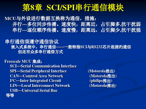
➢ 单工:1根数据线
➢ 全双工:2根数据线 (常用)
➢ 半双工:1根数据线
5. RS-232C串行通信原则
采用负逻辑:逻辑“1”:-15V~-3V ;逻辑“0”:+3V~+15V 传播距离≤30m,通信速率≤20Kbps 接口:9芯;常用3线:地(GND)、发送数据(TXD)、接受数据(RXD)
地址 寄存器名称与缩写
SPIS0PI工S作PI1模式 $030种D8: 主$机00模F0式控制寄存器1(SPICR1) $00D9 从$机00模F1式控制寄存器2(SPICR2) $00DA双$工00模F2式波特率寄存器(SPIBR)
$00DB $00F3 状态寄存器(SPISR)
访问 权限
基本功能
SCI旳寄存器设置 (1)SCI波特率寄存器---SCIxBDH、SCIxBDL
(共16位,13位有效)
高8位SCIBDH Bit7 Bit6 Bit5 Bit4 Bit3 Bit2 Bit1 Bit0
\
\
\ SBR12 SBR11 SBR10 SBR9 SBR8
低8位SCIBDL Bit7 Bit6 Bit5 Bit4 Bit3 Bit2 Bit1 Bit0
(4) SCI数据寄存器---SCIxDRH、SCIxDRL
高位SCIDRH Bit7
BitBit1
Bit0
R8
T8
\
\
\
\
\
\
低位SCIDRL Bit7 Bit6 Bit5 Bit4 Bit3 Bit2 Bit1 Bit0
R7/T7 R6/T6 R5/T5 R4/T4 R3/T3 R2/T2 R1/T1 R0/T0