AT24C1024
AT24系列的读写注意事项
AT24系列的读写注意事项AT24系列的读写注意事项所看过的对24系列I2C读写时序描述最准确最容易理解的资料,尤其是关于主从器件的应答描述和页写描述,看完后明白了很多。
关于页写的描述,网络上绝大部分范程都没提到页写时的数据地址必须是每页的首地址才能准确写入,而且如果写入超过一页的数据会循环覆盖当前页的数据。
关于IIC总线I2C总线:i2c总线是Philips 公司首先推出的一种两线制串行传输总线。
它由一根数据线(SDA)和一根时钟线(SDL)组成。
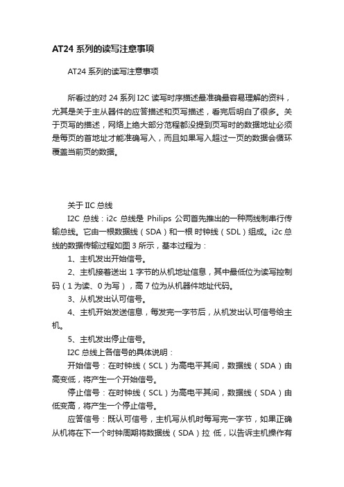
i2c总线的数据传输过程如图3所示,基本过程为:1、主机发出开始信号。
2、主机接着送出1字节的从机地址信息,其中最低位为读写控制码(1为读、0为写),高7位为从机器件地址代码。
3、从机发出认可信号。
4、主机开始发送信息,每发完一字节后,从机发出认可信号给主机。
5、主机发出停止信号。
I2C总线上各信号的具体说明:开始信号:在时钟线(SCL)为高电平其间,数据线(SDA)由高变低,将产生一个开始信号。
停止信号:在时钟线(SCL)为高电平其间,数据线(SDA)由低变高,将产生一个停止信号。
应答信号:既认可信号,主机写从机时每写完一字节,如果正确从机将在下一个时钟周期将数据线(SDA)拉低,以告诉主机操作有效。
在主机读从机时正确读完一字节后,主机在下一个时钟周期同样也要将数据线(SDA)拉低,发出认可信号,告诉从机所发数据已经收妥。
(注:读从机时主机在最后1字节数据接收完以后不发应答,直接发停止信号)。
注意:在I2C通信过程中,所有的数据改变都必须在时钟线SCL 为低电平时改变,在时钟线SCL为高电平时必须保持数据SDA信号的稳定,任何在时钟线为高电平时数据线上的电平改变都被认为是起始或停止信号。
作为一种非易失性存储器(NVM),24系列EEPROM使用的很普遍,一般作为数据量不太大的数据存储器。
下面总结一下其应用的一些要点。
从命名上看,24CXX中XX的单位是kbit,如24C08,其存储容量为8k bit,即1k Byte=1024 Byte。
串行EEPROM AT24CXX芯片资料
串行EEPROM AT24CXX芯片资料AT24CXX是美国ATMEL公司的低功耗CMOS串行EEPROM,典型的型号有AT24C01A/02/04/08/16等5种,它们的存储容量分别是1024/2048/4096/8192/16384位;也就是128/256/512/1024/2048字节;使用电压级别有5V,2.7V,2.5V,1.8V;本文主要介绍常用的AT24C02即256字节存储器的使用;它具有工作电压宽(2.5~5.5V)、擦写次数多(大于10000次)、写入速度快(小于10ms)等特点。
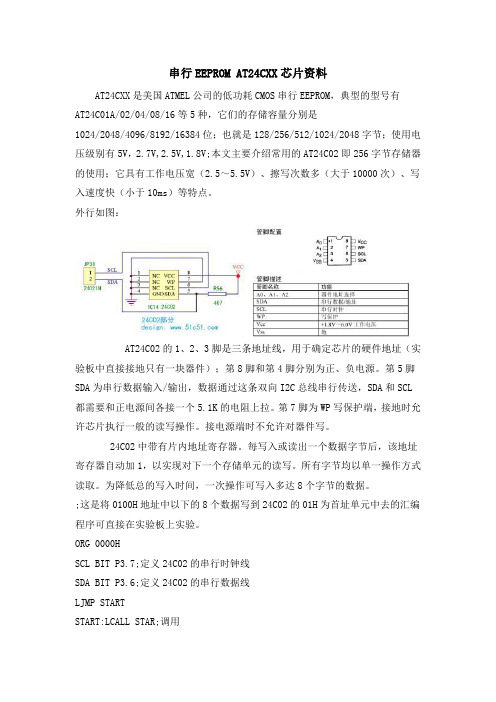
外行如图:AT24C02的1、2、3脚是三条地址线,用于确定芯片的硬件地址(实验板中直接接地只有一块器件);第8脚和第4脚分别为正、负电源。
第5脚SDA为串行数据输入/输出,数据通过这条双向I2C总线串行传送,SDA和SCL都需要和正电源间各接一个5.1K的电阻上拉。
第7脚为WP写保护端,接地时允许芯片执行一般的读写操作。
接电源端时不允许对器件写。
24C02中带有片内地址寄存器。
每写入或读出一个数据字节后,该地址寄存器自动加1,以实现对下一个存储单元的读写。
所有字节均以单一操作方式读取。
为降低总的写入时间,一次操作可写入多达8个字节的数据。
;这是将0100H地址中以下的8个数据写到24C02的01H为首址单元中去的汇编程序可直接在实验板上实验。
ORG 0000HSCL BIT P3.7;定义24C02的串行时钟线SDA BIT P3.6;定义24C02的串行数据线LJMP STARTSTART:LCALL STAR;调用MOV R2,#08H;一个数据有8位MOV DPTR,#0100H;定义源数据的位置LOOP:MOV A,#00HMOVC A,@A+DPTRLCALL SDATALCALL ACKJC LOOPINC DPTRDJNZ R2,LOOPLCALL STOP;调用停止子程序STAR:SETB SDASETB SCLNOPNOPNOPNOPCLR SDANOPNOPNOPNOPCLR SCLRETSDATA:MOV R0,#08HLOOP0:RLC AMOV SDA,CNOPNOPSETB SCLNOPNOPNOPCLR SCLDJNZ R0,LOOP0 RETACK:SETB SDA NOPNOPSETB SCL NOPNOPNOPNOPMOV C,SDA CLR SCLRETSTOP:CLR SDA NOPNOPNOPNOPSETB SCL NOPNOPNOPNOPSETB SDANOPNOPNOPRETORG 0100HDB 0A0H,10H,01H,02H,03H,04H,05H,06HEND读写子程序如下:;写串行E2PROM子程序XEPR; R3=10100000(命令1010+器件3位地址+读/写。
四片AT24C1024组成的存储器

料中均 有介绍 , 因此一般使 用起 来都 会得 心应 手的。然而 , 多块
这 样 的 芯 片 组 成 的 存 储器 其 使 用 方 法 在 各 类 刊 物 中 的介 绍 并 不
多见。笔者因水 文 自动 化测报业务需要 ,选用 了四片该 型号 的
E P OM 组 成 了容 量 为 5 2 B 的可 移 动 式 固 态 存 储器 。 表 面 ER 1K 从 上 看 , 四芯 片 组成 的 存 储 器 和 单 芯 片组 成 的 存 储 器 读 写 时序 等
维普资讯
四 A e 4组I 髓 T 4 12 0 f l l 曩储■
农 日忠
A 2 C1 2 T 4 0 4是 At l 司 生 产 的 大 容 量 串 行 E P 0M , me 公 ER 其 容 量 为 1 8 B 这 类 串行 E P 0M 单 一 芯 片组 成 的存 储 器 是 K 。 2 ER 最 常 见 的一 种 使 用 方 法 ,这 种 使 用 方 法 在 各 类 刊 物 和 厂 商 的 资
聿 l
{ B J
1 4
l
午
第
维普资讯
之 后 按 顺 序 存 入 第 二 块 ,第 二 块 数 据 占 满 之 后 按 顺 序 存 入 第 三 块 , 此 类 推 直 到 第 四块 存 满 为止 。 为 实 现 这 一 目的 , 数 据 写 依 在
R 2 2电平 。 S3 根据 AT 4 1 2 2 C 4的结构特点 , 0 一个 l C总线 可以连 接两块这样 的芯片。因此 , 选用 C U的 P . P 12至 P . 4个 I 15共 / 0
1 模 拟 两 组 l 总 线 与 四 片 E P 0M 组 成 的 存 储 器 相 连 接 , 7线 C ER 其 中 : 1 、 15为 第 一 组 l 线 与 U 、 5相 连 接 , 15为 数 P. P. 6 C总 3U P. 据 线 连 接 E P 0M 的 S A, 1 为 时 钟 线 连 接 E P 0M 的 ER D P. 4 ER S K: 12 P . 为 第 二 组 l 总 线 与 U 、 6相 连 接 , 12为 数 C P .、 1 3 C 4U P.
AT24C1024介绍

AT24C10242 线串行EEPROM特性低电压操作:2.7(Vcc=2.7V to 5.5V)内部组织:131,072*8 位=1M2 线串行接口施密特触发器,噪声抑制滤波输入双向数据传输协议时钟速率:400kHz(2.7V)和1MHz(5V) 硬件写保护引脚和软件数据保护256 字节页写模式(允许部分页面写入)随机和顺序读写模式自定义写周期(5ms)高可靠性:耐久力:写周期/页100,000 次数据保留:40 年8 引脚PDIP,8 引脚有铅SOIC 封装,8 引脚无铅阵列和8 引脚球状dBGA 封装描述AT24C1024 提供1,048,567 位的串行可电擦除和可编程只读存储器(EEPROM),它的每8 位组成一个字节,共131,072 个字节。
该设备的级联功能允许多达2 个设备共亨同一条2- 线总线。
该设备适合用于许多工业和商业,应用必要的低功耗和低电压的操作。
该器件可提供节省空间的8 引脚PDIP,8 引脚有铅SOIC 封装,8 引脚无铅阵列和8 引脚球状dBGA 封装。
另外,这一系列产品允许在2.7V(2.7V~5.5V)下工作。
绝对最大额定值:工作温度:-55~+125存储温度:-65~+150任何引脚的对地电压:-1.0V~+7.0V最大工作电压:6.25V 直流输出电流:5.0mA注意:强制高出“绝对最大额定值”可能导致设备的永久损坏。
设备的压力等级和功能操作只有在这些或超出本规范所标明的其他任何条件下是不允许的。
长时间工作在绝对最大额定值的条件下可能影响设备的可靠性。
引脚描述:串行时钟(SCL):SCL 的输入是在时钟的上升沿数据进入每个EEPROM 设备和下降沿数据输出每个设备。
串行数据(SDA):SDA 引脚是双向串行数据传输的。
这个引脚是漏极输出的,可以与其它的漏极开路或集电极开路的设备线或。
器件/ 页地址(A1 ):A1 引脚是设备的输入地址,它能够通过导线与不兼容的设备AT24C128/256/512 连接。
AT24cxx协议
AT24C02是由ATMEL公司提供的,IIC总线串行EEPROM(electronic eraser programmer read only memory),其容量为2kbit(256B),工作电压在2.7v"5.5v 之间,生产工艺是CMOS。
一般数字芯片都在左下角和右上角为GND,VCC。
容量的计算方法:AT24Cxx :01"1024 容量= xx * 1kbit。
写入过程:AT24C系列EEPROM芯片的固定部分为1010,A2,A1,A0引脚接高低电平后得到确定的3位编码,形成7位编码即为该器件的地址码。
单片机进行写操作时,首先发送该器件的7位地址码和写方向位”0”(共8位,即一个字节),发送完后释放SDA线并在SCL线上产生第9个时钟信号。
被选中的存储器器件在确认是自己的地址后,在SDA线上产生一个应答信号作为响应,单片机收到应答后就可以传送数据了。
传送数据时,单片机首先发送一个字节的被写入存储器的首地址,收到存储器器件的应答后,单片机就逐个发送数据字节,但每发送一个字节后都要等待应答。
AT24C系列片内地址在接收到每一个数据字节地址后自动加1,在芯片的“一次装载字节数”限度内,只需输入首地址。
装载字节数超过芯片的“一次装载字节数”时,数据地址将“上卷”,前面的数据将被覆盖。
字节写:页写:读入过程:单片机先发送该器件的7位地址码和写方向位“0”(“伪写”),发送完后释放SDA线并在SCL线上产生第9个时钟信号。
被选中的存储器器件在确认是自己的地址后,在SDA线上产生一个应答信号作为回应。
然后,再发一个字节的要读出器件的存储区的首地址,收到应答后,单片机要重复一次起始信号并发出器件地址和读方向位(“1”),收到器件应答后就可以读出数据字节,每读出一个字节,单片机都要回复应答信号。
当最后一个字节数据读完后,单片机应返回以“非应答”(高电平),并发出终止信号以结束读出操作。
基于Proteus的IIC器件AT24C1024的应用

关 键 词 :rt sE P O D 1b 0 温 度 传感 器 Poe ; E R M; S 8 2 ; u
电可擦 除可编 程 E P O 在应用 系统 中既可 的 P.和 P.模拟 I ER M 3 0 3 1 I 口与 A 2 C 04连接 , C接 T4 12
{
一
由软件对其内容进行随机读写, 又可在芯片断电的 情况 下长时 间保存 信息, 因此 兼备 了 R M 和 R A OM 的特点。E P OM有串行和并行 两大类 ,并行 ER E PO E R M存储容量较大, 读写方法简单, 但价格较 高适 用于信息量较多的场合。串行 E P OM结构 ER 简单紧凑' 价格低廉担 其读写方法复杂存 储单元较 小 般用于掉电情况下需要保存或一些数据需要 在线修改的场合这 类数据不多却很重要若使 用常 规的 R M芯片, A 就必须附带一套性能可靠的掉电 保护系统这不仅增加了线路设计的复杂性同 时也 给设备的运行和维护带来了诸多不便。同时 Po r— tu 软件是一款单片机软硬件设计仿真平台, es 能实 时仿 真 多种 单 片机 芯片 ,如 5 单 片 机 系列 、 V 1 AR 单 片 机 系列 、I 片 机 系列 及 Am 单 片 机 系列 PC单 r 等 , 少 学 习单片 机 的成 本 , 可达 到 良好 的学 可减 又 习效 果 。 1 4 2C系列 串行 E P O E R M介 绍 2C系列 串行 E P O 除具 有一 般 串行 4 ER M EP O E R M的体积小 、 功耗低 、 工作电压允许范围宽 等特 点外j 具有 型号多 、 大 、 总线 协议 、 丕 容量 二 占用 0口线少 、 容量扩展配置极其灵活方便、 读写操作 相对简单等特点 。本 系统 中使用的是 2 C 0 4 4 12 ( 2 k)生产 工艺 是 C S 艺 作 电压 在 1 ~ 1 4b, 0 MO T . 8 5 V之间2 C系列有两种封装形式: . 5 4 8脚封装和 1 4 脚封装 。 国 目前开发 用量最 多的封装 形式 是 8 我 脚 PI D P封装,脚 P I 8 DP封装中 A A1、2为器件地 0、 A 址选择位这 3个引脚配置成不同的编码直在同一 串行总线上最多可扩展 8片同一容量或不同容量 的 2 C系列串行 E P OM芯片。WP E  ̄ 为硬 4 ER f S 件写保护控制端( 测试端) 个引脚, 这 各个公 司生产 的有所不同洧 的公司将其定义为脉冲的上升沿将 数据写入 E P 下降沿将数据从 E P O E RO E R M中 读出。S A为串行数据输入输出端 漏极开路驱动, D 容量扩展时, 可以将多片 2 C系列 S A引脚直接 4 D 相连,实际使用时要加一个上拉电阻-C V C和 G D N 分别是 电源和地 。 2 T 4 2 2 C 0 4硬件 电路 的应用 设计 A 1 系统应用电路如图 1 所示, 时钟芯片接 P 端 l 口的 P . P .和 P . 1、1 0 1 1 2引脚 , 提供实时时间; 温度传 感器接 P 端 口的 P ., l 1 测量外界的温度; 7 由于 5 1 单片机没有 I I 口,可以利用单片机的 P 端口 C接 3
基于Proteus的IIC器件AT24C1024的应用
基于Proteus的IIC器件AT24C1024的应用作者:袁易君来源:《中国新技术新产品》2008年第24期摘要:本文采用软件仿真平台Proteus介绍了AT24C1024 EEPROM的使用及其特点,以及在具有DS1302时钟芯片、DS18b20温度传感器的具体应用系统中的使用,本系统对每隔一段时间的温度进行了存储。
关键词:Proteus;EEPROM;DS18b20;温度传感器电可擦除可编程EEPROM 在应用系统中既可由软件对其内容进行随机读写,又可在芯片断电的情况下长时间保存信息, 因此兼备了RAM 和ROM 的特点。
EEPROM 有串行和并行两大类,并行EEPROM 存储容量较大,读写方法简单,但价格较高,适用于信息量较多的场合。
串行EEPROM结构简单紧凑,价格低廉,但其读写方法复杂,存储单元较小,一般用于掉电情况下需要保存或一些数据需要在线修改的场合,这类数据不多却很重要,若使用常规的RAM芯片,就必须附带一套性能可靠的掉电保护系统,这不仅增加了线路设计的复杂性,同时也给设备的运行和维护带来了诸多不便。
同时Proteus软件是一款单片机软硬件设计仿真平台,能实时仿真多种单片机芯片,如51单片机系列、AVR单片机系列、PIC单片机系列及Arm单片机系列等,可减少学习单片机的成本,又可达到良好的学习效果。
124C系列串行EEPROM介绍24C系列串行EEPROM除具有一般串行EEPROM 的体积小、功耗低、工作电压允许范围宽等特点外,还具有型号多、容量大、二总线协议、占用I/ O 口线少、容量扩展配置极其灵活方便、读写操作相对简单等特点。
本系统中使用的是24C1024(1024kb) ,生产工艺是CMOS 工艺,工作电压在1.8~5.5V 之间,24C系列有两种封装形式:8 脚封装和14 脚封装。
我国目前开发用量最多的封装形式是8脚PDIP 封装,8 脚PDIP封装中A0 、A1 、A2 为器件地址选择位,这3 个引脚配置成不同的编码值,在同一串行总线上最多可扩展8 片同一容量或不同容量的24C 系列串行EEPROM 芯片。
AT24Cxx中文数据手册
AT24C01A/02/04/08A/16A提供1024/2048/4096/8192/16384个连续的可擦除的位,以及由每8位组成一个字节的可编程只读存储器(EEPROM),其分别提供128/256/512/1024/2048个字节。
该设备适用在许多低功耗和低电压操作的工业和商业应用中。
1引脚描述1.1串行时钟(SCL)SCL输入用于正向输出边缘时钟信号到每个EEPROM设备,以及每个设备输出的反向边缘时钟数据。
1.2串行数据(SDA)SDA引脚是用于串行数据双向传输。
该引脚为开漏输出,同时可以与其他开漏极或集电极开路器件进行线或。
1.3设备/页地址(A2,A1,A0)对于AT24C01A和AT24C02,A2、A1和A0引脚是配置器件的硬件地址输入。
一根总线上可以连接多达八个1K / 2K的设备(器件寻址部分详细讨论了器件寻址)。
AT24C04使用A2和A1引脚作为硬件地址输入,在一根总线上有4个4K 的设备可用来寻址。
A0引脚没有连接。
AT24C08A只使用A2引脚作为硬件地址输入,在一根总线上有2个8K 的设备可用来寻址。
A0和A1引脚没有连接。
AT24C16A不使用设备地址引脚,这限制了一根总线上只能挂一个设备。
A0、A1和A2引脚没有连接。
1.4写保护(WP)AT24C01A / 02 / 04 / 08A/ 16A有一个写保护引脚,提供硬件数据保护。
写保护引脚允许正常读/写操作时连接到GND。
当写保护引脚连接到VCC,写保护功能启用和操作如下表所示。
2设备操作2.1时钟和数据转换SDA引脚通常情况下拉高。
SDA引脚上的数据只能在SCL低时间段内更改,而启动条件或停止条件在SCL为高时进行。
2.2启动条件在任何其他指令之前,SDA由高变为低,且SCL为高。
2.3停止条件SDA由低变为高,且SCL为高。
在读取序列之后,执行停止命令后EEPROM进入备用电源模式。
2.4应答所有地址和数据字都是从EEPROM串行发送和接收8位字节。
中文数据手册AT24C系列
最小 1,000,000 100 2000 100
最大
单位 周期/字节 年 V mA
参考测试模式 MIL-STD-883 测试方法 1033 MIL-STD-883 测试方法 1008 MIL-STD-883 测试方法 3015 JEDEC 标准 17
3
广州周立功单片机发展有限公司 Tel
020
38730976
38730977
Fax 38730925
直流操作特性 Vcc=+1.8V 符号 ICC ISB ILI ILO VIL VIH VOL1 VOL2 +6.0V 除非特别说明 最小 典型 最大 3 0 10 10 1 Vcc 0.7 Vcc 0.3 Vcc+0.5 0.4 0.5 单位 mA A A A V V V V IOL=3 mA IOL=1.5 mA 测试条件 FSCL=100KHz VIN=0 ~Vcc VIN=0 ~Vcc VOUT=0 ~Vcc 参数 电源电流 备用电流(Vcc=5.0V) 输入漏电流 输出漏电流 输入低电压 输入高电压 输出低电压 输出低电压
1
广州周立功单片机发展有限公司 Tel
020
38730976
38730977
Fax 38730925
CAT24WC01/02/04/08/16 1K/2K/4K/8K/16K 位串行 E PROM
2
特性
I2C 总线协议
I2C 总线协议定义如下
5
广州周立功单片机发展有限公司 Tel
020
38730976
38730977
Fax 38730925
1 只有在总线空闲时才允许启动数据传送 2 在数据传送过程中 钟线为高电平时 起始信号 时钟线保持高电平期间 数据线电平从高到低的跳变作为 I2C 总线的起始信号 停止信号 时钟线保持高电平期间 数据线电平从低到高的跳变作为 I2C 总线的停止信号 图1 总线时序 当时钟线为高电平时 数据线必须保持稳定状态 不允许有跳变 时 数据线的任何电平变化将被看作总线的起始或停止信号
EEPROM---AT24Cxx应用介绍
EEPROM---AT24Cxx应⽤介绍结论:1、读写AT24CXX芯⽚,根据容量有多种⽅式:⼀、容量为AT24C01~AT24C16,⾸先发送设备地址(8位地址),再发送数据地址(8位地址),再发送或者接受数据。
⼆、AT24C32/AT24C64~AT24C512,⾸先发送设备地址(8位地址),再发送⾼位数据地址,再发送地位数据地址,再发送或者接受数据。
三、容量AT24C1024的芯⽚,是把容量⼀和容量⼆的⽅法结合,设备地址中要⽤⼀位作为数据地址位,存储地址长度是17位。
2、它的设备地址根据容量不同有区别: 1)、AT24C01~AT24C16:这⼀类⼜分为两类,分别为AT24C01/AT24C02和AT24C04~AT24C16;他们的设备地址为⾼7位,低1位⽤来作为读写标⽰位,1为读,0为写。
*1*、AT24C01/AT24C02。
AT24C01/AT24C02的A0、A1、A2引脚作为7位设备地址的低三位,⾼4为固定为1010B,低三位A0、A1、A2确定了AT24CXX的设备地址,所以⼀根I2C线上最⼤可以接8个AT24CXX,地址为1010000B~1010111B。
*2*、AT24C04~AT24C16的 A0、A1、A2只使⽤⼀部分,不⽤的悬空或者接地(数据⼿册中写的是悬空不接)。
举例:AT24C04只⽤A2、A1引脚作为设备地址,另外⼀位A0不⽤悬空,发送地址中对应的这位(A0)⽤来写⼊页寻址的页⾯号,⼀根I2C线上最⼤可以接4个,地址为101000xB~101011xB 2)、AT24C32/AT24C64:和AT24C01/AT24C02⼀样,区别是,发送数据地址变成16位。
注意事项:对AT24C32来说,WP置⾼,则只有四分之⼀受保护,即0x0C00-0x0FFF。
也就是说保护区为1KBytes。
对于低地址的四分之三,则不保护。
所以,如果数据较多时,可以有选择地存储。
- 1、下载文档前请自行甄别文档内容的完整性,平台不提供额外的编辑、内容补充、找答案等附加服务。
- 2、"仅部分预览"的文档,不可在线预览部分如存在完整性等问题,可反馈申请退款(可完整预览的文档不适用该条件!)。
- 3、如文档侵犯您的权益,请联系客服反馈,我们会尽快为您处理(人工客服工作时间:9:00-18:30)。
1Features•Low-voltage Operation –2.7 (V CC = 2.7V to 5.5V)•Internally Organized 131,072 x 8•2-wire Serial Interface•Schmitt Triggers, Filtered Inputs for Noise Suppression •Bi-directional Data Transfer Protocol•400 kHz (2.7V) and 1 MHz (5V) Clock Rate•Write Protect Pin for Hardware and Software Data Protection •256-byte Page Write Mode (Partial Page Writes Allowed)•Random and Sequential Read Modes •Self-timed Write Cycle (5 ms Typical)•High Reliability–Endurance: 100,000 Write Cycles/Page –Data Retention: 40 Years•8-lead PDIP , 8-lead EIAJ SOIC, 8-lead LAP and 8-ball dBGA TM PackagesDescriptionThe AT24C1024 provides 1,048,576 bits of serial electrically erasable and program-mable read only memory (EEPROM) organized as 131,072 words of 8 bits each. The device’s cascadable feature allows up to 2 devices to share a common 2-wire bus. The device is optimized for use in many industrial and commercial applications where low-power and low-voltage operation are essential. The devices are available in space-saving 8-lead PDIP, 8-lead EIAJ SOIC, 8-lead Leadless Array (LAP) and 8-ball dBGA packages. In addition, the entire family is available in 2.7V (2.7V to 5.5V) versions.Pin ConfigurationsPin Name Function A1Address Input SDA Serial Data SCL Serial Clock Input WPWrite Protect NCNo Connect8-lead PDIP8-lead Leadless ArrayBottom View8-lead SOIC8-ball dBGABottom View2AT24C10241471H–SEEPR–03/03Block DiagramAbsolute Maximum Ratings*Operating Temperature..................................-55°C to +125°C *NOTICE:Stresses beyond those listed under “Absolute Maximum Ratings” may cause permanent dam-age to the device. This is a stress rating only and functional operation of the device at these or any other conditions beyond those indicated in the operational sections of this specification is not implied. Exposure to absolute maximum rating conditions for extended periods may affect device reliability.Storage Temperature.....................................-65°C to +150°C Voltage on Any Pinwith Respect to Ground.....................................-1.0V to +7.0V Maximum Operating Voltage ..........................................6.25V DC Output Current........................................................5.0 mA3AT24C10241471H–SEEPR–03/03Pin DescriptionSERIAL CLOCK (SCL): The SCL input is used to positive edge clock data into each EEPROM device and negative edge clock data out of each device.SERIAL DATA (SDA): The SDA pin is bi-directional for serial data transfer. This pin is open-drain driven and may be wire-ORed with any number of other open-drain or open-collector devices.DEVICE/PAGE ADDRESSES (A1): The A1 pin is a device address input that can be hard-wired or left not connected for hardware compatibility with AT24C128/256/512. When the A1pin is hardwired, as many as two 1024K devices may be addressed on a single bus system (device addressing is discussed in detail under the Device Addressing section). When the pin is not hardwired, the default A1 is zero.WRITE PROTECT (WP): The hardware Write Protect pin is useful for protecting the entire contents of the memory from inadvertent write operations. The write-protect input, when tied to GND, allows normal write operations. When WP is tied high to V CC , all write operations to the memory are inhibited. If left unconnected, WP is internally pulled down to GND. Switching WP to V CC prior to a write operation creates a software write-protect function.Memory OrganizationAT24C1024, 1024K SERIAL EEPROM: The 1024K is internally organized as 512 pages of 256 bytes each. Random word addressing requires a 17-bit data word address.4AT24C10241471H–SEEPR–03/03Pin Capacitance (1)DC CharacteristicsNote:1.V IL min and V IH max are reference only and are not tested.Applicable over recommended operating range from T A = 25°C, f = 1.0 MHz, V CC = +2.7V.Symbol Test ConditionMax Units Conditions C I/O Input/Output Capacitance (SDA)8pF V I/O = 0V C IN Input Capacitance (A 1, SCL)6pFV IN = 0VApplicable over recommended operating range from: T AI = -40°C to +85°C, V CC = +2.7V to +5.5V, T AC = 0°C to +70°C,V CC = +2.7V to +5.5V (unless otherwise noted).Symbol Parameter Test ConditionMin TypMax Units V CC Supply Voltage 2.75.5V I CC Supply Current V CC = 5.0V READ at 400 kHz 2.0mA I CC Supply Current V CC = 5.0V WRITE at 400 kHz 5.0mA I SB Standby Current V CC = 2.7V V IN = V CC or V SS3.0µA V CC = 5.5V 6.0µA I LI Input Leakage Current V IN = V CC or V SS 0.10 3.0µA I LO Output Leakage CurrentV OUT = V CC or V SS0.053.0µA V IL Input Low Level (1)-0.6V CC x 0.3V V IH Input High Level (1)V CC x 0.7V CC + 0.5V V OL Output Low LevelV CC = 3.0VI OL = 2.1 mA0.4V5AT24C10241471H–SEEPR–03/03AC Characteristics2.AC measurement conditions:R L (connects to V CC ): 1.3 k Ω (2.7V , 5V)Input pulse voltages: 0.3 V CC to 0.7 V CC Input rise and fall times: ≤50 nsInput and output timing reference voltages: 0.5 V CCApplicable over recommended operating range from T A = -40°C to +85°C, V CC = +2.7V to +5.5V, C L = 100 pF (unless otherwise noted). Test conditions are listed in Note 2.Symbol ParameterTest Conditions MinMax Units f SCL Clock Frequency, SCL 4.5V ≤ V CC ≤ 5.5V 2.7V ≤ V CC ≤ 5.5V 1000400kHz t LOW Clock Pulse Width Low 4.5V ≤ V CC ≤ 5.5V 2.7V ≤ V CC ≤ 5.5V 0.41.3µs t HIGH Clock Pulse Width High 4.5V ≤ V CC ≤ 5.5V 2.7V ≤ V CC ≤ 5.5V 0.40.6µs t AA Clock Low to Data Out Valid4.5V ≤ V CC ≤5.5V 2.7V ≤ V CC ≤ 5.5V 0.050.050.550.9µs t BUF Time the bus must be free before a new transmission can start (1) 4.5V ≤ V CC ≤ 5.5V 2.7V ≤ V CC ≤ 5.5V 0.51.3µs t HD.STA Start Hold Time 4.5V ≤ V CC ≤ 5.5V 2.7V ≤ V CC ≤ 5.5V 0.250.6µs t SU.STA Start Setup Time 4.5V ≤ V CC ≤ 5.5V 2.7V ≤ V CC ≤ 5.5V0.250.6µs t HD.DAT Data In Hold Time 0µs t SU.DA T Data In Setup Time 100ns t R Inputs Rise Time (1)0.3µs t F Inputs Fall Time (1) 4.5V ≤ V CC ≤ 5.5V 2.7V ≤ V CC ≤ 5.5V 100300ns t SU.STO Stop Setup Time 4.5V ≤ V CC ≤ 5.5V 2.7V ≤ V CC ≤ 5.5V0.250.6µs t DH Data Out Hold Time 50ns t WRWrite Cycle Time10ms Endurance (1) 5.0V , 25°C, Page Mode100KWrite Cycles6AT24C10241471H–SEEPR–03/03Device OperationCLOCK and DATA TRANSITIONS: The SDA pin is normally pulled high with an external device. Data on the SDA pin may change only during SCL low time periods (refer to Data Validity timing diagram). Data changes during SCL high periods will indicate a start or stop condition as defined below.START CONDITION: A high-to-low transition of SDA with SCL high is a start condition which must precede any other command (refer to Start and Stop Definition timing diagram).STOP CONDITION: A low-to-high transition of SDA with SCL high is a stop condition. After a read sequence, the Stop command will place the EEPROM in a standby power mode (refer to Start and Stop Definition timing diagram).ACKNOWLEDGE: All addresses and data words are serially transmitted to and from the EEPROM in 8-bit words. The EEPROM sends a zero during the ninth clock cycle to acknowl-edge that it has received each word.STANDBY MODE: The AT24C1024 features a low-power standby mode which is enabled: a)upon power-up and b)after the receipt of the STOP bit and the completion of any internal operations.MEMORY RESET: After an interruption in protocol, power loss or system reset, any 2-wire part can be reset by following these steps:1.Clock up to 9 cycles,2.Look for SDA high in each cycle while SCL is high.3.Create a start condition.7AT24C10241471H–SEEPR–03/03Bus Timing (SCL: Serial Clock, SDA: Serial Data I/O)Write Cycle Timing (SCL: Serial Clock, SDA: Serial Data I/O)Note:1.The write cycle time t WRis the time from a valid stop condition of a write sequence to the end of the internal clear/write cycle.8AT24C10241471H–SEEPR–03/03Data ValidityStart and Stop DefinitionOutput Acknowledge9AT24C10241471H–SEEPR–03/03DeviceAddressingThe 1024K EEPROM requires an 8-bit device address word following a start condition to enable the chip for a read or write operation (refer to Figure 1). The device address word con-sists of a mandatory one, zero sequence for the first five most significant bits as shown. This is common to all 2-wire EEPROM devices.The 1024K uses the one device address bit, A1, to allow up to two devices on the same bus.The A1 bit must compare to the corresponding hardwired input pin. The A1 pin uses an inter-nal proprietary circuit that biases it to a logic low condition if the pin is allowed to float.The seventh bit (P 0) of the device address is a memory page address bit. This memory page address bit is the most significant bit of the data word address that follows. The eighth bit of the device address is the read/write operation select bit. A read operation is initiated if this bit is high and a write operation is initiated if this bit is low.Upon a compare of the device address, the EEPROM will output a zero. If a compare is not made, the device will return to a standby state.DATA SECURITY: The AT24C1024 has a hardware data protection scheme that allows the user to write-protect the entire memory when the WP pin is at V CC .WriteOperationsBYTE WRITE: To select a data word in the 1024K memory requires a 17-bit word address.The word address field consists of the P 0 bit of the device address, then the most significant word address followed by the least significant word address (refer to Figure 2)A write operation requires the P 0 bit and two 8-bit data word addresses following the device address word and acknowledgment. Upon receipt of this address, the EEPROM will again respond with a zero and then clock in the first 8-bit data word. Following receipt of the 8-bit data word, the EEPROM will output a zero. The addressing device, such as a microcontroller,then must terminate the write sequence with a stop condition. At this time the EEPROM enters an internally timed write cycle, T WR , to the nonvolatile memory. All inputs are disabled during this write cycle and the EEPROM will not respond until the write is complete (refer to Figure 2).PAGE WRITE: The 1024K EEPROM is capable of 256-byte page writes.A page write is initiated the same way as a byte write, but the microcontroller does not send a stop condition after the first data word is clocked in. Instead, after the EEPROM acknowledges receipt of the first data word, the microcontroller can transmit up to 255 more data words. The EEPROM will respond with a zero after each data word received. The microcontroller must ter-minate the page write sequence with a stop condition (refer to Figure 3).The data word address lower 8 bits are internally incremented following the receipt of each data word. The higher data word address bits are not incremented, retaining the memory page row location. When the word address, internally generated, reaches the page boundary, the following byte is placed at the beginning of the same page. If more than 256 data words are transmitted to the EEPROM, the data word address will “roll over” and previous data will be overwritten. The address “rollover” during write is from the last byte of the current page to the first byte of the same page.ACKNOWLEDGE POLLING: Once the internally timed write cycle has started and the EEPROM inputs are disabled, acknowledge polling can be initiated. This involves sending a start condition followed by the device address word. The read/write bit is representative of the operation desired. Only if the internal write cycle has completed will the EEPROM respond with a zero, allowing the read or write sequence to continue.10AT24C10241471H–SEEPR–03/03ReadOperationsRead operations are initiated the same way as write operations with the exception that the read/write select bit in the device address word is set to one. There are three read operations:current address read, random address read and sequential read.CURRENT ADDRESS READ: The internal data word address counter maintains the last address accessed during the last read or write operation, incremented by one. This address stays valid between operations as long as the chip power is maintained. The address “rollover”during read is from the last byte of the last memory page, to the first byte of the first page.Once the device address with the read/write select bit set to one is clocked in and acknowl-edged by the EEPROM, the current address data word is serially clocked out. The microcontroller does not respond with an input zero but does generate a following stop condi-tion (refer to Figure 4).RANDOM READ: A random read requires a “dummy” byte write sequence to load in the data word address. Once the device address word and data word address are clocked in and acknowledged by the EEPROM, the microcontroller must generate another start condition.The microcontroller now initiates a current address read by sending a device address with the read/write select bit high. The EEPROM acknowledges the device address and serially clocks out the data word. The microcontroller does not respond with a zero but does generate a fol-lowing stop condition (refer to Figure 5).SEQUENTIAL READ: Sequential reads are initiated by either a current address read or a ran-dom address read. After the microcontroller receives a data word, it responds with an acknowledge. As long as the EEPROM receives an acknowledge, it will continue to increment the data word address and serially clock out sequential data words. When the memory address limit is reached, the data word address will “roll over” and the sequential read will con-tinue. The sequential read operation is terminated when the microcontroller does not respondwith a zero, but does generate a following stop condition (refer to Figure 6).11AT24C10241471H–SEEPR–03/03Figure 1. Device AddressFigure 2. Byte WriteFigure 3. Page WriteFigure 4.Current Address Read12AT24C10241471H–SEEPR–03/03Figure 5. Random ReadFigure 6.Sequential Read13AT24C10241471H–SEEPR–03/03Note:For 2.7V devices used in the 4.5V to 5.5V range, please refer to performance values in the AC and DC Characteristics tables.Ordering InformationOrdering Code PackageOperation Range A T24C1024-10CI-2.7A T24C1024C1-10CI-2.7A T24C1024-10PI-2.7A T24C1024W-10SI-2.7A T24C1024-10UI-2.78CN38CN18P38S28U8Industrial (-40°C to 85°C)Package Type8CN38-lead, 0.230" Wide, Leadless Array Package (LAP)8CN18-lead, 0.300" Wide, Leadless Array Package (LAP)8P38-lead, 0.300" Wide, Plastic Dual In-line Package (PDIP)8S28-lead, 0.200" Wide, Plastic Gull Wing Small Outline Package (EIAJ SOIC)8U88-ball, die Ball Grid Array Package (dBGA)Options-2.7Low Voltage (2.7V to 5.5V)14AT24C10241471H–SEEPR–03/03Packaging Information8CN3 – LAP15AT24C10241471H–SEEPR–03/038CN1 – LAP16AT24C10241471H–SEEPR–03/038P3 – PDIP17AT24C10241471H–SEEPR–03/038S2 – EIAJ SOIC18AT24C10241471H–SEEPR–03/038U8 – dBGA1471H–SEEPR–03/03xMDisclaimer: Atmel Corporation makes no warranty for the use of its products, other than those expressly contained in the Company’s standard warranty which is detailed in Atmel’s Terms and Conditions located on the Company’s web site. The Company assumes no responsibility for any errors which may appear in this document, reserves the right to change devices or specifications detailed herein at any time without notice, and does not make any commitment to update the information contained herein. No licenses to patents or other intellectual property of Atmel are granted by the Company in connection with the sale of Atmel products, expressly or by implication. Atmel’s products are not authorized for use as critical components in life support devices or systems.Atmel CorporationAtmel Operations 2325 Orchard ParkwaySan Jose, CA 95131Tel: 1(408) 441-0311Fax: 1(408) 487-2600Regional Headquarters Europe Atmel Sarl Route des Arsenaux 41Case Postale 80CH-1705 FribourgSwitzerlandTel: (41) 26-426-5555Fax: (41) 26-426-5500Asia Room 1219Chinachem Golden Plaza77 Mody Road TsimshatsuiEast KowloonHong KongTel: (852) 2721-9778Fax: (852) 2722-1369Japan 9F, Tonetsu Shinkawa Bldg.1-24-8 Shinkawa Chuo-ku, Tokyo 104-0033Japan Tel: (81) 3-3523-3551Fax: (81) 3-3523-7581Memory 2325 Orchard Parkway San Jose, CA 95131Tel: 1(408) 441-0311Fax: 1(408) 436-4314Microcontrollers 2325 Orchard Parkway San Jose, CA 95131Tel: 1(408) 441-0311Fax: 1(408) 436-4314La Chantrerie BP 7060244306 Nantes Cedex 3, FranceTel: (33) 2-40-18-18-18Fax: (33) 2-40-18-19-60ASIC/ASSP/Smart Cards Zone Industrielle 13106 Rousset Cedex, France Tel: (33) 4-42-53-60-00Fax: (33) 4-42-53-60-011150 East Cheyenne Mtn. Blvd.Colorado Springs, CO 80906Tel: 1(719) 576-3300Fax: 1(719) 540-1759Scottish Enterprise Technology ParkMaxwell BuildingEast Kilbride G75 0QR, ScotlandTel: (44) 1355-803-000Fax: (44) 1355-242-743RF/Automotive Theresienstrasse 2Postfach 353574025 Heilbronn, Germany Tel: (49) 71-31-67-0Fax: (49) 71-31-67-23401150 East Cheyenne Mtn. Blvd.Colorado Springs, CO 80906Tel: 1(719) 576-3300Fax: 1(719) 540-1759Biometrics/Imaging/Hi-Rel MPU/High Speed Converters/RF Datacom Avenue de Rochepleine BP 12338521 Saint-Egreve Cedex, FranceTel: (33) 4-76-58-30-00Fax: (33) 4-76-58-34-80e-mailliterature@Web Site © Atmel Corporation 2003. All rights reserved. Atmel ® and combinations thereof, are the registeredtrademarks, and dBG A ™ is the trademark of Atmel Corporation or its subsidiaries. Other terms and productnames may be the trademarks of others.。