格恩半导体产品规格书
sic437规格书
sic437规格书SIC437规格书是指由美国半导体工业协会(SIA)和欧洲电子元器件工业协会(EECA)共同制定的半导体产品的标准规范。
该规格书的制定旨在规范半导体产品的设计、生产、测试和质量控制等方面的标准,以确保半导体产品的性能和质量达到了一定的水平,同时也方便半导体相关行业企业的生产和管理。
具体而言,SIC437规格书包括了以下内容:1.产品类型:此规范适用于单晶硅、多晶硅、氮化硅等材料生产的半导体知识产权产品,例如集成电路、光电器件、功率半导体等。
2.产品特性:该规范对半导体产品的电气和物理特性进行了严格的规定,例如工作电压、电流、功率、温度范围、封装方式、尺寸等。
3.测试规范:该规范对半导体产品的测试方法和测试环节进行了规定,包括测试设备、测试方式、测试流程、测试结果分析等。
4.质量标准:该规范对半导体产品的生产过程和质量进行了详细的规范,包括原材料的选择、生产工艺的规范、质量控制流程等,以确保产品的质量稳定和可靠。
5.其他:该规范还包括了一些其他的工业标准,例如耐受性规范、环境适应性规范、封装标准等,以保证半导体产品的可靠性和性能稳定性。
SIC437规格书对于半导体相关企业和行业来说非常重要,它不仅规范了产品的设计和生产过程,提高了产品的质量和稳定性,也为行业间的交流和合作提供了一个标准的基础。
同时,在国际贸易中,也可以作为一项交流和合作的重要工具,为企业之间的商业合作提供更为通畅的环境。
总之,SIC437规格书的制定凝聚了国际半导体行业的智慧和努力,它的出现标志着半导体行业产品标准化的进一步发展和提高,对于半导体企业和相关行业的可持续发展有着积极的推动作用。
半导体传感器ADG333ABRZ中文规格书

ADG408/ADG409Data Sheet Rev. D | Page 4 of 15 B Version T Version Parameter+25°C −40°C to +85°C +25°C −55°C to +125°C Unit Test Conditions/Comments POWER REQUIREMENTSI DD1 1 μA typ V IN = 0 V, V EN = 0 V 5 5 μA max I SS1 1 μA typ 5 5 μA max I DD 100100 μA typ V IN = 0 V, V EN = 2.4 V200 500 200 500 μA max1 Guaranteed by design, not subject to production test.SINGLE SUPPLYV DD = 12 V , V SS = 0 V , GND = 0 V , unless otherwise noted. Table 2.B VersionT Version Parameter+25°C −40°C to+85°C +25°C −55°C to +125°C Unit Test Conditions/Comments ANALOG SWITCHAnalog Signal Range 0 to V DD0 to V DD V R ON 9090Ω typ V D = 3 V, 10 V, I S = –1 mA LEA K AGE CURRENTSSource Off Leakage I S (Off) ±0.5 ±50 ±0.5±50 nA max VD = 8 V/0 V, V S = 0 V/8 V; see Figure 19 Drain Off Leakage I D (Off)V D = 8 V/0 V, V S = 0 V/8 V; see Figure 20 ADG408 ±1 ±100 ±1±100 nA max ADG409±1 ±50±1±50nA max Channel On Leakage I D , I S (On)V S = V D = 8 V/0 V; see Figure 21 ADG408 ±1 ±100 ±1±100 nA max ADG409±1 ±50±1±50nA max DIGITAL INPUTSInput High Voltage, V INH 2.42.4V min Input Low Voltage, V INL 0.80.8V max Input CurrentI INL or I INH ±10±10μA max V IN = 0 or V DD C IN, Digital Input Capacitance 8 8pF typ f = 1 MHz DYNAMIC CHARACTERISTICS1t TRANSITION 130130ns typ R L = 300 Ω, C L = 35 pF; V S1 = 8 V/0 V, V S8 = 0 V/8 V; see Figure 22 t OPEN1010ns typ R L = 300 Ω, C L = 35 pF; V S = 5 V; see Figure 23 t ON (EN)140140ns typ R L = 300 Ω C L = 35 pF; V S = 5 V; see Figure 24 t OFF (EN)6060ns typ R L = 300 Ω, C L = 35 pF; V S = 5 V; see Figure 24 Charge Injection55pC typ V S = 0 V, R S = 0 Ω, C L = 10 nF; see Figure 25Off Isolation –75–75dB typ R L = 1 kΩ f = 100 kHz;V EN = 0 V; see Figure 26ADG408/ADG409Data Sheet Rev. D | Page 14 of 15 OUTLINE DIMENSIONSCOMPLIANT TO JEDEC STANDARDS MS-001-BB0.1953-07-2014-DFigure 28. 16-Lead Plastic Dual In-Line Package [PDIP]Narrow Body(N-16)Dimensions shown in inches and (millimeters) CONTROLLING DIMENSIONS ARE IN MILLIMETERS; INCH DIMENSIONS (IN PARENTHESES) ARE ROUNDED-OFF MILLIMETER EQUIVALENTS FOR REFERENCE ONLY AND ARE NOT APPROPRIATE FOR USE IN PLIANT TO JEDEC STANDARDS MS-012-AC 3.80 (0.1496)PLANE 0.31 (0.0122)1.75 (0.0689)1.27 (0.0500)0.40 (0.0157)0.17 (0.0067)COPLANARITY 0.10 45°Figure 29. 16-Lead Standard Small Outline Package [SOIC_N]Narrow Body(R-16)Dimensions shown in millimeters and (inches)。
EMD2 UMD2N IMD2A 双极性半导体电子器件商品说明书

TransistorsRev.B 1/3General purpose(dual digital transistors)EMD2 / UMD2N / IMD2Az Features z Dimensions (Unit : mm) 1) Both the DTA124E chip and DTC124E chip in a EMTor UMT or SMT package.2) Mounting possible with EMT6 or UMT6 or SMT6 automatic mounting machines.3) Transistor elements are independent, eliminating interference.4) Mounting cost and area can be cut in half.z StructureEpitaxial planar typeNPN / PNP silicon transistor (Built-in resistor type)The following characteristics apply to both the DTr 1 andDTr 2, however, the “−” sign on DTr 2 values for the PNPtype have been omitted.z Equivalent circuitz Absolute maximum ratings (T a = 25°C)ParameterSymbol Limits Unit V CC 50V 40VV IN −10I O 30mAI C (Max.)100Tj 150˚C Tstg−55 to +150˚CPd EMD2, UMD2N 150 (TOTAL)mW IMD2A 300 (TOTAL)∗1∗2Supply voltage Input voltageOutput currentJunction temperature Storage temperaturePowerdissipation ∗1 120mW per element must not be exceeded.∗2 200mW per element must not be exceeded.TransistorsRev.B 2/3z Electrical characteristics (T a = 25°C)ParameterSymbol I I R 1G I R 2/R 1Min.−3−−−15.4560.8−−0.1−−22−10.5−0.30.360.528.6−1.2V V CC =5V, I O =100µA V O =0.2V, I O=5mA I O =10mA, I I =0.5mA V I =5VV CC =50V, V I =0V −V O =5V, I O =5mAV mA µA k Ω−−−Typ.Max.Unit ConditionsV I (off)V I (on)V O (on)I O (off)f T −250−V CE =10V, I E =−5mA, f =100MHz ∗MHz Transition frequency of the deviceInput voltage Output voltage Input current Output current Input resistance DC current gain Transition frequencyResistance ratioz Electrical characteristic curves DTr 1 (NPN)I N P U T V O L T A G E : V I (o n ) (V )OUTPUT CURRENT : I O(A)Fig.1 Input voltage vs. output current(ON characteristics)INPUT VOLTAGE : V I (off) (V)O U T P U T C U R R E N T : I o(A )120050010020501025Fig.2 Output current vs. input voltage(OFF characteristics)OUTPUT CURRENT : I O (A)D C C U R RE N T G A I N : G IFig.3 DC current gain vs. outputcurrentTransistorsRev.B 3/3OUTPUT CURRENT : I O (A)O U T P U T V O L T A G E : V O (o n ) (V )Fig.4 Output voltage vs. outputcurrentDTr 2 (PNP)I NP U T V O L T A G E : V I (o n ) (V )OUTPUT CURRENT : I O (A)−−−−−−−−−−Fig.5 Input voltage vs. output current(ON characteristics)−−1−−−−200−500−100−20−50−10−2−5INPUT VOLTAGE : V I (off) (V)O U T P U T C U R R E N T :I o (A )Fig.6 Output current vs. input voltage(OFF characteristics)D C C U R RE N T G A I N : G IOUTPUT CURRENT : I O (A)−Fig.7 DC current gain vs. outputcurrent−−−−−−−−−−−OUTPUT CURRENT : I O (A)O U T P U T V O L T A G E : V O (o n ) (V )Fig.8 Output voltage vs. outputcurrentAppendix1-Rev2.0Thank you for your accessing to ROHM product informations.More detail product informations and catalogs are available, please contact your nearest sales office.ROHM Customer Support SystemTHE AMERICAS / EUROPE / ASIA / JAPANContact us : webmaster@rohm.co.jpAppendix。
半导体传感器MUX08FSZ中文规格书

ADuM1400/ADuM1401/ADuM1402Data SheetRev. L | Page 20 of 31DIN V VDE V 0884-10 (VDE V 0884-10) INSULATION CHARACTERISTICS These isolators are suitable for reinforced electrical isolation only within the safety limit data. Maintenance of the safety data is ensured by protective circuits. The asterisk (*) marking on packages denotes DIN V VDE V 0884-10 approval. Table 11.DescriptionConditions Symbol Characteristic Unit Installation Classification per DIN VDE 0110For Rated Mains Voltage ≤ 150 V rmsI to IV For Rated Mains Voltage ≤ 300 V rmsI to III For Rated Mains Voltage ≤ 400 V rmsI to II Climatic Classification 40/105/21 Pollution Degree per DIN VDE 0110, Table 12 Maximum Working Insulation VoltageV IORM 560 V peak Input to Output Test Voltage, Method B1V IORM × 1.875 = V PR , 100% production test, t m = 1 sec, partial discharge < 5 pC V PR 1050 V peak Input to Output Test Voltage, Method AV IORM × 1.6 = V PR , t m = 60 sec, partial discharge < 5 pC V PR After Environmental Tests Subgroup 1896 V peak After Input and/or Safety Test Subgroup 2and Subgroup 3V IORM × 1.2 = V PR , t m = 60 sec, partial discharge < 5 pC 672 V peak Highest Allowable OvervoltageTransient overvoltage, t TR = 10 seconds V TR 4000 V peak Safety Limiting ValuesMaximum value allowed in the event of a failure (see Figure 4) Case TemperatureT S 150 °C Side 1 CurrentI S1 265 mA Side 2 CurrentI S2 335 mA Insulation Resistance at T SV IO = 500 V R S >109Ω CASE TEMPERATURE (°C)S A F E T Y -L I M I T I N G C U R R E N T (m A )003503002502001501005050100150200SIDE #1SIDE #203786-004Figure 4. Thermal Derating Curve, Dependence of Safety Limiting Values with Case Temperature per DIN V VDE V 0884-10 RECOMMENDED OPERATING CONDITIONS Table 12.Parameter Rating Operating Temperature (T A )1 −40°C to +105°C Operating Temperature (T A )2 −40°C to +125°C Supply Voltages (V DD1, V DD2)1, 3 2.7 V to 5.5 V Supply Voltages (V DD1, V DD2)2, 3 3.0 V to 5.5 V Input Signal Rise and Fall Times 1.0 ms 1 Does not apply to ADuM1400W , ADuM1401W , and ADuM1402W automotive grade versions. 2 Applies to ADuM1400W , ADuM1401W , and ADuM1402W automotive grade versions. 3 All voltages are relative to their respective ground. See the DC Correctness and Magnetic Field Immunity section for information on immunity to external magnetic fields.ADuM1400/ADuM1401/ADuM1402 Data SheetRev. L | Page 30 of 31OUTLINE DIMENSIONSCONTROLLING DIMENSIONS ARE IN MILLIMETERS;INCH DIMENSIONS (IN PARENTHESES)ARE ROUNDED-OFF MILLIMETER EQUIVALENTS FOR REFERENCE ONLY AND ARE NOT APPROPRIATE FOR USE IN PLIANT TO JEDEC STANDARDS MS-013-AA03-27-2007-B Figure 24. 16-Lead Standard Small Outline Package [SOIC_W] Wide Body (RW-16) Dimensions shown in millimeters and (inches) ORDERING GUIDEModel1, 2, 3, 4Number of Inputs, V DD1 Side Number of Inputs, V DD2 Side Maximum Data Rate (Mbps) Maximum Propagation Delay, 5 V (ns) Maximum Pulse Width Distortion (ns) Temperature Range Package Description Package Option ADuM1400ARW4 0 1 100 40 −40°C to +105°C 16-Lead SOIC_W RW-16 ADuM1400BRW4 0 10 50 3 −40°C to +105°C 16-Lead SOIC_W RW-16 ADuM1400CRW4 0 90 32 2 −40°C to +105°C 16-Lead SOIC_W RW-16 ADuM1400ARWZ4 0 1 100 40 −40°C to +105°C 16-Lead SOIC_W RW-16 ADuM1400BRWZ4 0 10 50 3 −40°C to +105°C 16-Lead SOIC_W RW-16 ADuM1400CRWZ4 0 90 32 2 −40°C to +105°C 16-Lead SOIC_W RW-16 ADuM1400WSRWZ4 0 1 100 40 −40°C to +125°C 16-Lead SOIC_W RW-16 ADuM1400WTRWZ4 0 10 34 3 −40°C to +125°C 16-Lead SOIC_W RW-16 ADuM1401ARW3 1 1 100 40 −40°C to +105°C 16-Lead SOIC_W RW-16 ADuM1401BRW3 1 10 50 3 −40°C to +105°C 16-Lead SOIC_W RW-16 ADuM1401CRW3 1 90 32 2 −40°C to +105°C 16-Lead SOIC_W RW-16 ADuM1401ARWZ3 1 1 100 40 −40°C to +105°C 16-Lead SOIC_W RW-16 ADuM1401BRWZ3 1 10 50 3 −40°C to +105°C 16-Lead SOIC_W RW-16 ADuM1401CRWZ3 1 90 32 2 −40°C to +105°C 16-Lead SOIC_W RW-16 ADuM1401WSRWZ3 1 1 100 40 −40°C to +125°C 16-Lead SOIC_W RW-16 ADuM1401WTRWZ3 1 10 34 3 −40°C to +125°C 16-Lead SOIC_W RW-16 ADuM1402ARW2 2 1 100 40 −40°C to +105°C 16-Lead SOIC_W RW-16 ADuM1402BRW2 2 10 503 −40°C to +105°C 16-Lead SOIC_W RW-16 ADuM1402CRW2 2 90 32 2 −40°C to +105°C 16-Lead SOIC_W RW-16 ADuM1402ARWZ2 2 1 100 40 −40°C to +105°C 16-Lead SOIC_W RW-16 ADuM1402BRWZ2 2 10 503 −40°C to +105°C 16-Lead SOIC_W RW-16 ADuM1402CRWZ2 2 90 32 2 −40°C to +105°C 16-Lead SOIC_W RW-16 ADuM1402WSRWZ2 2 1 100 40 −40°C to +125°C 16-Lead SOIC_W RW-16 ADuM1402WTRWZ2 2 10 343 −40°C to +125°C 16-Lead SOIC_W RW-16 EVAL-ADuMQSEBZ Evaluation Board 1Z = RoHS Compliant Part. 2 W = Qualified for Automotive Applications. 3 Tape and reel are available. The addition of an -RL suffix designates a 13” (1,000 units) tape and reel option. 4 No tape and reel option is available for the ADuM1400CRW or ADuM1402BRW models.。
FPGA可编程逻辑器件芯片10AS027E3F29E2LG中文规格书
Send Feedback
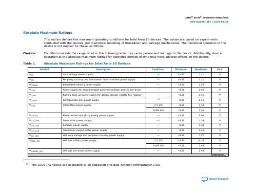
Intel® Arria® 10 Device Datasheet A10-DATASHEET | 2020.06.26
Symbol VCCPLL_HPS IOUT
TJ TSTG
HPS PLL power supply DC output current per pin
Description
This table lists the maximum allowed input overshoot voltage and the duration of the overshoot voltage as a percentage of device lifetime. The LVDS I/O values are applicable to the VREFP_ADC and VREFN_ADC I/O pins.
Caution:
Conditions outside the range listed in the following table may cause permanent damage to the device. Additionally, device operation at the absolute maximum ratings for extended periods of time may have adverse effects on the device.
Maximum 1.21 1.21 1.36 2.46 2.46 2.46 4.10 2.46 2.46 1.34 1.34 2.46 1.27 4.10 2.46 2.46
Unit V V V V V V V V V V V V V V V V
半导体传感器ADG1608BRUZ中文规格书

ADF4116/ADF4117/ADF4118Rev. D | Page 7 of 28PIN CONFIGURATION AND FUNCTION DESCRIPTIONSCPCPGNDAGNDAV DDRF IN ARF IN BFL ODV DD MUXOUT LE CE REF IN DGNDCLK DATA V P 00392-003Figure 3. Pin Configuration Table 4. Pin Function DescriptionsPin No. Mnemonic Description1 FL O Fast Lock Switch Output. This can be used to switch an external resistor to change the loop filter bandwidthand speed up locking the PLL.2 CP Charge Pump Output. When enabled, this provides the ± I CP to the external loop filter, which in turn drives theexternal VCO.3 CPGND Charge Pump Ground. This is the ground return path for the charge pump.4 AGND Analog Ground. This is the ground return path for the prescaler.5 RF IN B Complementary Input to the RF Prescaler. This point should be decoupled to the ground plane with a smallbypass capacitor, typically 100 pF. See Figure 26.6 RF IN A Input to the RF Prescaler. This small signal input is ac-coupled from the VCO.7 AV DD Analog Power Supply. This can range from 2.7 V to 5.5 V. Decoupling capacitors to the analog ground planeshould be placed as close as possible to this pin. AV DD must have the same value as DV DD .8 REF IN Reference Input. This is a CMOS input with a nominal threshold of V DD /2 and an equivalent input resistance of 100 kΩ.See Figure 25. The oscillator input can be driven from a TTL or CMOS crystal oscillator, or it can be ac-coupled.9 DGND Digital Ground.10 CE Chip Enable. A logic low on this pin powers down the device and puts the charge pump output into three-statemode. Taking the pin high powers up the device depending on the status of the power-down bit F2.11 CLK Serial Clock Input. This serial clock is used to clock in the serial data to the registers. The data is latched into the21-bit shift register on the CLK rising edge. This input is a high impedance CMOS input.12 DATA Serial Data Input. The serial data is loaded MSB first with the two LSBs as the control bits. This input is a highimpedance CMOS input.13 LE Load Enable, CMOS Input. When LE goes high, the data stored in the shift registers is loaded into one of the fourlatches, the latch being selected using the control bits.14 MUXOUT This multiplexer output allows either the lock detect, the scaled RF, or the scaled reference frequency to beaccessed externally.15 DV DD Digital Power Supply. This can range from 2.7 V to 5.5 V. Decoupling capacitors to the digital ground plane (1 μF , 1 nF)should be placed as close as possible to this pin. For best performance, the 1 μF capacitor should be placed within 2 mm of the pin. The placing of the 1 nF capacitor is less critical, but should still be within 5 mm of the pin. DV DD must have the same value as AV DD .16 V P Charge Pump Power Supply. This should be greater than or equal to V DD . In systems where V DD is 3 V, this supply canbe set to 6 V and used to drive a VCO with a tuning range of up to 6 V.ADF4116/ADF4117/ADF4118Rev. D | Page 13 of 28 PHASE FREQUENCY DETECTOR (PFD)AND CHARGE PUMPThe PFD takes inputs from the R counter and N counter and produces an output proportional to the phase and frequency difference between them. Figure 28 is a simplified schematic of the PFD. The PFD includes a fixed delay element that sets the width of the antibacklash pulse. This is typically 3 ns. This pulse ensures that there is no dead zone in the PFD transfer function and gives a consistent reference spur level.00392-028Figure 28. PFD Simplified Schematic and Timing (In Lock)MUXOUT AND LOCK DETECT The output multiplexer on the ADF411x family allows the user to access various internal points on the chip. The state of MUXOUT is controlled by M3, M2, and M1 in the function latch. Figure 33 shows the full truth table. Figure 29 shows the MUXOUT section in block diagram form. 00392-029Figure 29. MUXOUT Circuit Lock DetectMUXOUT can be programmed for both digital lock detect and analog lock detect.Digital lock detect is active high. It is set high when the phase error on three consecutive phase detector cycles is less than 15 ns. It stays set high until a phase error greater than 25 ns isdetected on any subsequent PD cycle.The N channel, open-drain, analog lock detect should be operated with an external pull-up resistor of 10 kΩ nominal. When lock is detected, it is high with narrow low going pulses.INPUT SHIFT REGISTER The ADF411x family digital section includes a 21-bit input shiftregister, a 14-bit R counter, and an 18-bit N counter, comprising a 5-bit A counter and a 13-bit B counter. Data is clocked into the 21-bit shift register on each rising edge of CLK. The data is clocked in MSB first. Data is transferred from the shift register to one of four latches on the rising edge of LE. The destination latch is determined by the state of the two control bits (C2, C1) in the shift register. These are the two LSBs, DB1 and DB0, as shown in the timing diagram in Figure 2. The truth table for these bits is shown in Figure 34. Table 5 summarizes how the latches are programmed.Table 5. Programming Data LatchesControl Bits C2C1 Data Latch 00 R Counter 01 N Counter (A and B) 10 Function Latch 1 1 Initialization Latch。
Nexperia 半导体产品说明书

Important noticeDear Customer,On 7 February 2017 the former NXP Standard Product business became a new company with the tradename Nexperia. Nexperia is an industry leading supplier of Discrete, Logic and PowerMOS semiconductors with its focus on the automotive, industrial, computing, consumer and wearable application marketsIn data sheets and application notes which still contain NXP or Philips Semiconductors references, use the references to Nexperia, as shown below.Instead of , / or /, use ************************************************************************,use *************************** (email)Replace the copyright notice at the bottom of each page or elsewhere in the document, depending on the version, as shown below:- © NXP N.V. (year). All rights reserved or © Koninklijke Philips Electronics N.V. (year). All rights reservedShould be replaced with:- © Nexperia B.V. (year). All rights reserved.If you have any questions related to the data sheet, please contact our nearest sales office via e-mail or telephone (details via ***************************). Thank you for your cooperation and understanding,Kind regards,Team NexperiaBUK7575-100AN-channel TrenchMOS standard level FETRev. 02 — 30 July 2009Product data sheet 1.Product profile1.1General descriptionStandard level N-channel enhancement mode Field-Effect Transistor (FET) in a plasticpackage using TrenchMOS technology. This product has been designed and qualified tothe appropriate AEC standard for use in automotive critical applications.1.2Features and benefitsLow conduction losses due to low on-state resistanceQ101 compliant Suitable for standard level gate drive sourcesSuitable for thermally demanding environments due to 175 °C rating1.3Applications12 V, 24 V and 42 V loadsAutomotive and general purposepower switchingMotors, lamps and solenoids1.4Quick reference dataTable 1.Quick referenceSymbol Parameter Conditions Min Typ Max Unit V DS drain-source voltage T j≥25°C; T j≤175°C--100VI D drain current V GS=10V; T mb=25°C;see Figure 1 and 3--23AP tot total powerdissipationT mb=25°C; see Figure 2--99W Avalanche ruggednessE DS(AL)S non-repetitivedrain-sourceavalanche energy I D=14A;V sup≤100V;R GS=50Ω; V GS=10V;T j(init)=25°C; unclamped--100mJStatic characteristicsR DSon drain-sourceon-state resistance V GS=10V; I D=13A;T j=175°C; see Figure 12and 13--187mΩV GS=10V; I D=13A;T j=25°C; see Figure 12and 13-6475mΩBUK7575-100A_2© NXP B.V. 2009. All rights reserved.Product data sheet Rev. 02 — 30 July 2009 2 of 132.Pinning information3.Ordering informationTable 2.Pinning information Pin Symbol Description Simplified outline Graphic symbol1G gate SOT78A (TO-220AB)2D drain 3S sourcembDmounting base; connected to drain12mb3Table 3.Ordering informationType numberPackage NameDescriptionVersionBUK7575-100ATO-220ABplastic single-ended package; heatsink mounted; 1 mounting hole; 3-lead TO-220ABSOT78ABUK7575-100A_2© NXP B.V. 2009. All rights reserved.Product data sheet Rev. 02 — 30 July 2009 3 of 134.Limiting valuesTable 4.Limiting values In accordance with the Absolute Maximum Rating System (IEC 60134).Symbol ParameterConditionsMin Max Unit V DS drain-source voltage T j ≥25°C; T j ≤175°C -100V V DGR drain-gate voltage R GS =20k Ω-100V V GS gate-source voltage -2020V I D drain current T mb =25°C; V GS =10V; see Figure 1 and 3-23A T mb =100°C; V GS =10V; see Figure 1-16.2A I DM peak drain current T mb =25°C; t p ≤10µs; pulsed; see Figure 3-92A P tot total power dissipation T mb =25°C; see Figure 2-99W T stg storage temperature -55175°C T j junction temperature -55175°C Source-drain diodeI S source current T mb =25°C-23A I SM peak source currentt p ≤10µs; pulsed; T mb =25°C-92A Avalanche ruggednessE DS(AL)Snon-repetitive drain-source avalanche energyI D =14A; V sup ≤100V; R GS =50Ω; V GS =10V; T j(init)=25°C; unclamped -100mJBUK7575-100A_2© NXP B.V. 2009. All rights reserved. Product data sheet Rev. 02 — 30 July 2009 4 of 13BUK7575-100A_2© NXP B.V. 2009. All rights reserved.Product data sheet Rev. 02 — 30 July 2009 5 of 135.Thermal characteristicsTable 5.Thermal characteristics Symbol ParameterConditionsMin Typ Max Unit R th(j-mb)thermal resistance from junction to mounting basesee Figure 4-- 1.5K/WR th(j-a)thermal resistance from junction to ambient-60-K/WBUK7575-100A_2© NXP B.V. 2009. All rights reserved.Product data sheet Rev. 02 — 30 July 2009 6 of 136.CharacteristicsTable 6.Characteristics Symbol Parameter ConditionsMin Typ Max Unit Static characteristicsV (BR)DSS drain-sourcebreakdown voltage I D =0.25mA;V GS =0V; T j =25°C 100--V I D =0.25mA;V GS =0V; T j =-55°C 89--V V GS(th)gate-source threshold voltageI D =1mA; V DS = V GS ; T j =175°C;see Figure 111--V I D =1mA; V DS = V GS ; T j =-55°C;see Figure 11-- 4.4V I D =1mA; V DS = V GS ; T j =25°C;see Figure 11234V I DSS drain leakage current V DS =100V; V GS =0V;T j =175°C --500µA V DS =100V; V GS =0V;T j =25°C -0.0510µA I GSS gate leakage current V DS =0V; V GS =20V; T j =25°C -2100nA V DS =0V; V GS =-20V; T j =25°C -2100nA R DSondrain-source on-state resistanceV GS =10V; I D =13A; T j =175°C;see Figure 12 and 13--187m ΩV GS =10V; I D =13A; T j =25°C;see Figure 12 and 13-6475m ΩDynamic characteristics C iss input capacitance V GS =0V;V DS =25V; f =1MHz; T j =25°C;see Figure 15-9071210pF C oss output capacitance -127150pF C rss reverse transfer capacitance -78110pF t d(on)turn-on delay time V DS =30V;R L =2.2Ω; V GS =10V; R G(ext)=5.6Ω; T j =25°C -8-ns t r rise time-39-ns t d(off)turn-off delay time -26-ns t f fall time -24-ns L Dinternal drain inductancefrom drain lead 6 mm from package to centre of die; T j =25°C- 4.5-nH from contact screw on mounting base to centre of die; T j =25°C- 3.5-nH L Sinternal source inductancefrom source lead to source bond pad; T j =25°C-7.5-nHSource-drain diode V SD source-drain voltage I S =25A;V GS =0V; T j =25°C;see Figure 14-0.85 1.2V t rr reverse recovery time I S =13A;dI S /dt =-100A/µs; V GS =-10V; V DS =30V;T j =25°C-64-ns Q rrecovered charge-120-nCBUK7575-100A_2© NXP B.V. 2009. All rights reserved. Product data sheet Rev. 02 — 30 July 20097 of 13BUK7575-100A_2© NXP B.V. 2009. All rights reserved. Product data sheet Rev. 02 — 30 July 20098 of 13BUK7575-100A_2© NXP B.V. 2009. All rights reserved. Product data sheet Rev. 02 — 30 July 20099 of 137.Package outlinePlastic single-ended package; heatsink mounted; 1 mounting hole; 3-lead TO-220AB SOT78AFig 16.Package outline SOT78A (TO-220AB)8.Revision historyTable 7.Revision historyDocument ID Release date Data sheet status Change notice SupersedesBUK7575-100A_220090730Product data sheet-BUK7575_7675_100A-01 Modifications:•The format of this data sheet has been redesigned to comply with the new identityguidelines of NXP Semiconductors.•Legal texts have been adapted to the new company name where appropriate.•Type number BUK7575-100A separated from data sheet BUK7575_7675_100A-01.20001024Product specification--BUK7575_7675_100A-01(9397 750 07623)9.Legal information9.1Data sheet status[1]Please consult the most recently issued document before initiating or completing a design.[2]The term 'short data sheet' is explained in section "Definitions".[3]The product status of device(s) described in this document may have changed since this document was published and may differ in case of multiple devices. The latest product status information is available on the Internet at URL .9.2DefinitionsDraft — The document is a draft version only. The content is still under internal review and subject to formal approval, which may result in modifications or additions. NXP Semiconductors does not give any representations or warranties as to the accuracy or completeness ofinformation included herein and shall have no liability for the consequences of use of such information.Short data sheet — A short data sheet is an extract from a full data sheet with the same product type number(s) and title. A short data sheet is intended for quick reference only and should not be relied upon to contain detailed and full information. For detailed and full information see the relevant full data sheet, which is available on request via the local NXP Semiconductors sales office. In case of any inconsistency or conflict with the short data sheet, the full data sheet shall prevail.9.3DisclaimersGeneral — Information in this document is believed to be accurate andreliable. However, NXP Semiconductors does not give any representations or warranties, expressed or implied, as to the accuracy or completeness of such information and shall have no liability for the consequences of use of such information.Right to make changes — NXP Semiconductors reserves the right to make changes to information published in this document, including withoutlimitation specifications and product descriptions, at any time and without notice. This document supersedes and replaces all information supplied prior to the publication hereof.Suitability for use — NXP Semiconductors products are not designed, authorized or warranted to be suitable for use in medical, military, aircraft, space or life support equipment, nor in applications where failure ormalfunction of an NXP Semiconductors product can reasonably be expected to result in personal injury, death or severe property or environmentaldamage. NXP Semiconductors accepts no liability for inclusion and/or use of NXP Semiconductors products in such equipment or applications and therefore such inclusion and/or use is at the customer’s own risk.Applications — Applications that are described herein for any of these products are for illustrative purposes only. NXP Semiconductors makes no representation or warranty that such applications will be suitable for the specified use without further testing or modification.Quick reference data — The Quick reference data is an extract of theproduct data given in the Limiting values and Characteristics sections of this document, and as such is not complete, exhaustive or legally binding. Limiting values — Stress above one or more limiting values (as defined in the Absolute Maximum Ratings System of IEC 60134) may cause permanent damage to the device. Limiting values are stress ratings only and operation of the device at these or any other conditions above those given in theCharacteristics sections of this document is not implied. Exposure to limiting values for extended periods may affect device reliability.Terms and conditions of sale — NXP Semiconductors products are sold subject to the general terms and conditions of commercial sale, as published at /profile/terms , including those pertaining to warranty, intellectual property rights infringement and limitation of liability, unlessexplicitly otherwise agreed to in writing by NXP Semiconductors. In case of any inconsistency or conflict between information in this document and such terms and conditions, the latter will prevail.No offer to sell or license — Nothing in this document may be interpreted or construed as an offer to sell products that is open for acceptance or the grant, conveyance or implication of any license under any copyrights, patents or other industrial or intellectual property rights.Export control — This document as well as the item(s) described herein may be subject to export control regulations. Export might require a prior authorization from national authorities.9.4TrademarksNotice: All referenced brands, product names, service names and trademarks are the property of their respective owners.TrenchMOS — is a trademark of NXP B.V.10.Contact informationFor more information, please visit: For sales office addresses, please send an email to: **********************Document status [1][2]Product status [3]DefinitionObjective [short] data sheet Development This document contains data from the objective specification for product development.Preliminary [short] data sheet Qualification This document contains data from the preliminary specification.Product [short] data sheetProductionThis document contains the product specification.11.Contents1Product profile. . . . . . . . . . . . . . . . . . . . . . . . . . .11.1General description . . . . . . . . . . . . . . . . . . . . . .11.2Features and benefits. . . . . . . . . . . . . . . . . . . . .11.3Applications . . . . . . . . . . . . . . . . . . . . . . . . . . . .11.4Quick reference data . . . . . . . . . . . . . . . . . . . . .12Pinning information. . . . . . . . . . . . . . . . . . . . . . .23Ordering information. . . . . . . . . . . . . . . . . . . . . .24Limiting values. . . . . . . . . . . . . . . . . . . . . . . . . . .35Thermal characteristics . . . . . . . . . . . . . . . . . . .56Characteristics. . . . . . . . . . . . . . . . . . . . . . . . . . .67Package outline. . . . . . . . . . . . . . . . . . . . . . . . .108Revision history. . . . . . . . . . . . . . . . . . . . . . . . .119Legal information. . . . . . . . . . . . . . . . . . . . . . . .129.1Data sheet status . . . . . . . . . . . . . . . . . . . . . . .129.2Definitions. . . . . . . . . . . . . . . . . . . . . . . . . . . . .129.3Disclaimers. . . . . . . . . . . . . . . . . . . . . . . . . . . .129.4Trademarks. . . . . . . . . . . . . . . . . . . . . . . . . . . .1210Contact information. . . . . . . . . . . . . . . . . . . . . .12Please be aware that important notices concerning this document and the product(s)described herein, have been included in section ‘Legal information’.© NXP B.V.2009.All rights reserved.For more information, please visit: Forsalesofficeaddresses,pleasesendanemailto:**********************。
半导体传感器AD7394ARZ中文规格书

ADuM1400/ADuM1401/ADuM1402 Data SheetRev. L | Page 28 of 31For example, at a magnetic field frequency of 1 MHz, the maximum allowable magnetic field of 0.2 kgauss induces a voltage of 0.25 V at the receiving coil. This is about 50% of the sensing threshold and does not cause a faulty output transition. Similarly, if such an event occurs during a transmitted pulse (and has the worst-case polarity), it reduces the received pulse from >1.0 V to 0.75 V—still well above the 0.5 V sensing threshold of the decoder. The preceding magnetic flux density values correspond to specific current magnitudes at given distances from the ADuM1400/ADuM1401/ADuM1402 transformers. Figure 20expresses these allowable current magnitudes as a function of frequency for selected distances. As shown, the ADuM1400/ ADuM1401/ADuM1402 are extremely immune and can be affected only by extremely large currents operated at high frequency very close to the component. For the 1 MHz example noted, one would have to place a 0.5 kA current 5 mm away from the ADuM1400/ADuM1401/ADuM1402 to affect the operation of the component.MAGNETIC FIELD FREQUENCY (Hz)M A X I M U M A L L O W A B L E C U R R E N T (k A )1k 10k 100M 100k 1M 10M 03786-020Figure 20. Maximum Allowable Current for Various Current-to-ADuM1400/ADuM1401/ADuM1402 Spacings Note that at combinations of strong magnetic field and high frequency, any loops formed by printed circuit board traces could induce error voltages sufficiently large enough to trigger the thresholds of succeeding circuitry. Care should be taken in the layout of such traces to avoid this possibility.POWER CONSUMPTIONThe supply current at a given channel of the ADuM1400/ ADuM1401/ADuM1402 isolator is a function of the supply voltage, the data rate of the channel, and the output load of the channel.For each input channel, the supply current is given by I DDI = I DDI (Q )f ≤ 0.5 f r I DDI = I DDI (D) × (2f − f r ) + I DDI (Q )f > 0.5 f r For each output channel, the supply current is given by I DDO = I DDO (Q ) f ≤ 0.5 f r I DDO = (I DDO (D ) + (0.5 × 10⁻³) × C L × V DDO ) × (2f − f r ) + I DDO (Q ) f > 0.5 f r where: I DDI (D), I DDO (D) are the input and output dynamic supply currents per channel (mA/Mbps). C L is the output load capacitance (pF). V DDO is the output supply voltage (V). f is the input logic signal frequency (MHz); it is half of the inputdata rate expressed in units of Mbps. f r is the input stage refresh rate (Mbps). I DDI (Q), I DDO (Q) are the specified input and output quiescent supply currents (mA).To calculate the total V DD1 and V DD2 supply current, the supply currents for each input and output channel corresponding to V DD1 and V DD2 are calculated and totaled. Figure 8 and Figure 9 provide per-channel supply currents as a function of data rate for an unloaded output condition. Figure 10 provides per-channel supply current as a function of data rate for a 15 pF output condition. Figure 11 through Figure 15 provide total V DD1 and V DD2 supply current as a function of data rate for ADuM1400/ADuM1401/ADuM1402 channel configurations.Data SheetADuM1400/ADuM1401/ADuM1402 Rev. L | Page 29 of 31 INSULATION LIFETIMEAll insulation structures eventually break down when subjected to voltage stress over a sufficiently long period. The rate of insulation degradation is dependent on the characteristics of the voltage waveform applied across the insulation. In addition to the testing performed by the regulatory agencies, Analog Devices carries out an extensive set of evaluations to determine the lifetime of the insulation structure within the ADuM1400/ ADuM1401/ADuM1402.Analog Devices performs accelerated life testing using voltage levels higher than the rated continuous working voltage. Accel-eration factors for several operating conditions are determined. These factors allow calculation of the time to failure at the actual working voltage. The values shown in Table 14 summarize the peak voltage for 50 years of service life for a bipolar ac operating condition and the maximum CSA/VDE approved working voltages. In many cases, the approved working voltage is higher than a 50-year service life voltage. Operation at these high working voltages can lead to shortened insulation life in some cases. The insulation lifetime of the ADuM1400/ADuM1401/ADuM1402 depends on the voltage waveform type imposed across the isolation barrier. The i Coupler insulation structure degrades at different rates depending on whether the waveform is bipolar ac, unipolar ac, or dc. Figure 21, Figure 22, and Figure 23 illustrate these different isolation voltage waveforms, respectively. Bipolar ac voltage is the most stringent environment. The goal of a 50-year operating lifetime under the ac bipolar condition determines the Analog Devices recommended maximum working voltage. In the case of unipolar ac or dc voltage, the stress on the insulation is significantly lower, which allows operation at higher working voltages while still achieving a 50-year service life. The working voltages listed in Table 14 can be applied while maintaining the 50-year minimum lifetime, provided the voltage conforms to either the unipolar ac or dc voltage cases. Any cross-insulation voltage waveform that does not conform to Figure 22 or Figure 23 should be treated as a bipolar ac waveform, and its peak voltage should be limited to the 50-year lifetime voltage value listed in Table 14. Note that the voltage presented in Figure 22 is shown as sinusoidal for illustration purposes only. It is meant to represent any voltage waveform varying between 0 V and some limiting value. The limiting value can be positive or negative, but the voltage cannot cross 0 V . 0V RATED PEAK VOLTAGE 03786-021Figure 21. Bipolar AC Waveform 0V RATED PEAK VOLTAGE 03786-022Figure 22. Unipolar AC Waveform 0V RATED PEAK VOLTAGE 03786-023Figure 23. DC Waveform。
- 1、下载文档前请自行甄别文档内容的完整性,平台不提供额外的编辑、内容补充、找答案等附加服务。
- 2、"仅部分预览"的文档,不可在线预览部分如存在完整性等问题,可反馈申请退款(可完整预览的文档不适用该条件!)。
- 3、如文档侵犯您的权益,请联系客服反馈,我们会尽快为您处理(人工客服工作时间:9:00-18:30)。
格恩半导体产品规格书
英文回答:
The specification sheet for the Geon Semiconductor product is a comprehensive document that outlines the technical details and performance characteristics of the product. It serves as a reference guide for customers, engineers, and other stakeholders who are interested in the product.
The specification sheet typically includes information such as the product's electrical and mechanical specifications, operating conditions, and performance parameters. It provides details about the product's voltage ratings, current ratings, power dissipation, and temperature range. Additionally, it may also include information about the product's package type, pin configuration, and recommended PCB layout.
For example, let's say we are looking at the
specification sheet for a Geon Semiconductor microcontroller. The sheet would provide details about the microcontroller's operating voltage range, maximum clock frequency, and number of I/O pins. It would also specify the microcontroller's flash memory size, RAM size, and any additional peripherals or features it may have, such as built-in analog-to-digital converters or communication interfaces.
Furthermore, the specification sheet may also include performance characteristics such as the microcontroller's power consumption in different operating modes, its response time for various operations, and its tolerance to external disturbances such as noise or temperature variations.
In addition to the technical specifications, the specification sheet may also provide information about the product's certifications, compliance with industry standards, and any special requirements or considerations for its usage. For example, it may specify the product's compliance with RoHS (Restriction of Hazardous Substances)
regulations or its suitability for specific applications or environments.
中文回答:
格恩半导体产品规格书是一份详尽的文档,概述了产品的技术
细节和性能特征。
它是供客户、工程师和其他相关人员参考的指南。
规格书通常包括产品的电气和机械规格、工作条件和性能参数
等信息。
它提供了有关产品的电压额定值、电流额定值、功耗和温
度范围等细节。
此外,它还可能包括有关产品的封装类型、引脚配
置和推荐的PCB布局的信息。
例如,假设我们正在查看格恩半导体微控制器的规格书。
规格
书将提供有关微控制器的工作电压范围、最大时钟频率和I/O引脚
数量的详细信息。
它还会指定微控制器的闪存大小、RAM大小以及
任何额外的外设或功能,例如内置的模数转换器或通信接口。
此外,规格书还可能包括性能特征,如微控制器在不同工作模
式下的功耗、各种操作的响应时间以及对噪声或温度变化等外部干
扰的容忍度。
除了技术规格外,规格书还可能提供有关产品的认证、符合行
业标准的情况以及使用时的任何特殊要求或注意事项的信息。
例如,它可能指定产品符合RoHS(有害物质限制)法规或其适用于特定应
用或环境的情况。
总之,格恩半导体产品规格书是一份重要的文档,为用户和利
益相关者提供了详细的产品信息,帮助他们了解产品的技术特性和
性能参数,并为正确使用产品提供指导。