加速度传感器使用方法说明书
Analog Devices ADXL335 三轴加速度传感器说明书
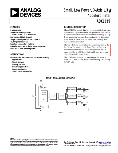
Small, Low Power, 3-Axis ±3 gAccelerometerADXL335Rev. BInformation furnished by Analog Devices is believed to be accurate and reliable. However , no responsibility is assumed by Analog Devices for its use, nor for any infringements of patents or other rights of third parties that may result from its use. Specifications subject to change without notice. No license is granted by implication or otherwise under any patent or patent rights of Analog Devices. T rademarks and registered trademarks are the property of their respective owners.One Technology Way, P.O. Box 9106, Norwood, M A 02062-9106, U.S.A.Tel: 781.329.4700 Fax: 781.461.3113 ©2009–2010 Analog Devices, Inc. All rights reserved.FEATURES3-axis sensingSmall, low profile package4 mm × 4 mm × 1.45 mm LFCSP Low power : 350 μA (typical)Single-supply operation: 1.8 V to 3.6 V 10,000 g shock survivalExcellent temperature stabilityBW adjustment with a single capacitor per axis RoHS/WEEE lead-free compliantAPPLICATIONSCost sensitive, low power, motion- and tilt-sensing applications Mobile devices Gaming systemsDisk drive protection Image stabilizationSports and health devicesGENERAL DESCRIPTIONThe ADXL335 is a small, thin, low power, complete 3-axis accel-erometer with signal conditioned voltage outputs. The product measures acceleration with a minimum full-scale range of ±3 g . It can measure the static acceleration of gravity in tilt-sensing applications, as well as dynamic acceleration resulting from motion, shock, or vibration.The user selects the bandwidth of the accelerometer using the C X , C Y , and C Z capacitors at the X OUT , Y OUT , and Z OUT pins. Bandwidths can be selected to suit the application, with a range of 0.5 Hz to 1600 Hz for the X and Y axes, and a range of 0.5 Hz to 550 Hz for the Z axis.The ADXL335 is available in a small, low profile, 4 mm ×4 mm × 1.45 mm, 16-lead, plastic lead frame chip scale package (LFCSP_LQ).FUNCTIONAL BLOCK DIAGRAMC DCFigure 1.ADXL335Rev. B | Page 2 of 16TABLE OF CONTENTSFeatures .............................................................................................. 1 Applications ....................................................................................... 1 General Description ......................................................................... 1 Functional Block Diagram .............................................................. 1 Revision History ............................................................................... 2 Specifications ..................................................................................... 3 Absolute Maximum Ratings ............................................................ 4 ESD Caution .................................................................................. 4 Pin Configuration and Function Descriptions ............................. 5 Typical Performance Characteristics ............................................. 6 Theory of Operation ...................................................................... 10 Mechanical Sensor ...................................................................... 10 Performance ................................................................................ 10 Applications Information .............................................................. 11 Power Supply Decoupling ......................................................... 11 Setting the Bandwidth Using C X , C Y , and C Z .......................... 11 Self-Test ....................................................................................... 11 Design Trade-Offs for Selecting Filter Characteristics: The Noise/BW Trade-Off .................................................................. 11 Use with Operating V oltages Other Than 3 V ........................... 12 Axes of Acceleration Sensitivity ............................................... 12 Layout and Design Recommendations ................................... 13 Outline Dimensions ....................................................................... 14 Ordering Guide .. (14)REVISION HISTORY1/10—Rev. A to Rev. BChanges to Figure 21 (9)7/09—Rev. 0 to Rev. AChanges to Figure 22 ........................................................................ 9 Changes to Outline Dimensions (14)1/09—Revision 0: Initial VersionADXL335Rev. B | Page 3 of 16SPECIFICATIONST A = 25°C, V S = 3 V , C X = C Y = C Z = 0.1 μF, acceleration = 0 g , unless otherwise noted. All minimum and maximum specifications are guaranteed. Typical specifications are not guaranteed. Table 1.Parameter Conditions M in Typ M ax Unit SENSOR INPUT Each axisMeasurement Range ±3 ±3.6g Nonlinearity % of full scale ±0.3 % Package Alignment Error ±1 Degrees Interaxis Alignment Error ±0.1 DegreesCross-Axis Sensitivity 1±1 % SENSITIVITY (RATIOMETRIC)2 Each axis Sensitivity at X OUT , Y OUT , Z OUT V S = 3 V 270 300 330 mV/gSensitivity Change Due to Temperature 3V S = 3 V ±0.01 %/°C ZERO g BIAS LEVEL (RATIOMETRIC) 0 g Voltage at X OUT , Y OUT V S = 3 V 1.35 1.5 1.65 V 0 g Voltage at Z OUT V S = 3 V 1.2 1.5 1.8 V 0 g Offset vs. Temperature ±1 m g /°C NOISE PERFORMANCE Noise Density X OUT , Y OUT 150 μg /√Hz rms Noise Density Z OUT 300 μg /√Hz rms FREQUENCY RESPONSE 4 Bandwidth X OUT , Y OUT 5 No external filter 1600 Hz Bandwidth Z OUT 5 No external filter 550 Hz R FILT Tolerance 32 ± 15% kΩ Sensor Resonant Frequency 5.5 kHz SELF-TEST 6 Logic Input Low +0.6 V Logic Input High +2.4 V ST Actuation Current +60 μA Output Change at X OUT Self-Test 0 to Self-Test 1 −150 −325 −600 mV Output Change at Y OUT Self-Test 0 to Self-Test 1 +150 +325 +600 mV Output Change at Z OUT Self-Test 0 to Self-Test 1 +150 +550 +1000 mV OUTPUT AMPLIFIER Output Swing Low No load 0.1 V Output Swing High No load 2.8 V POWER SUPPLY Operating Voltage Range 1.8 3.6 V Supply Current V S = 3 V 350 μA Turn-On Time 7 No external filter 1 ms TEMPERATURE Operating Temperature Range −40 +85 °C1 Defined as coupling between any two axes. 2Sensitivity is essentially ratiometric to V S . 3Defined as the output change from ambient-to-maximum temperature or ambient-to-minimum temperature. 4Actual frequency response controlled by user-supplied external filter capacitors (C X , C Y , C Z ). 5Bandwidth with external capacitors = 1/(2 × π × 32 kΩ × C). For C X , C Y = 0.003 μF, bandwidth = 1.6 kHz. For C Z = 0.01 μF, bandwidth = 500 Hz. For C X , C Y , C Z = 10 μF, bandwidth = 0.5 Hz. 6Self-test response changes cubically with V S . 7Turn-on time is dependent on C X , C Y , C Z and is approximately 160 × C X or C Y or C Z + 1 ms, where C X , C Y , C Z are in microfarads (μF).ADXL335Rev. B | Page 4 of 16ABSOLUTE MAXIMUM RATINGSTable 2.Parameter Rating Acceleration (Any Axis, Unpowered) 10,000 g Acceleration (Any Axis, Powered) 10,000 g V S −0.3 V to +3.6 V All Other Pins (COM − 0.3 V) to (V S + 0.3 V)Output Short-Circuit Duration(Any Pin to Common)Indefinite Temperature Range (Powered) −55°C to +125°C Temperature Range (Storage) −65°C to +150°CStresses above those listed under Absolute Maximum Ratings may cause permanent damage to the device. This is a stress rating only; functional operation of the device at these or any other conditions above those indicated in the operationalsection of this specification is not implied. Exposure to absolute maximum rating conditions for extended periods may affect device reliability.ESD CAUTIONADXL335Rev. B | Page 5 of 16PIN CONFIGURATION AND FUNCTION DESCRIPTIONS07808-003NOTES1. EXPOSED PAD IS NOT INTERNALLYCONNECTED BUT SHOULD BE SOLDERED FOR MECHANICAL INTEGRITY.NC = NO CONNECTNCST COM NCX OUT NC Y OUT NCC O MC O MC O MZ O U TN CV SV SN CFigure 2. Pin ConfigurationTable 3. Pin Function DescriptionsPin No. MnemonicDescription1 NC No Connect.12 ST Self-Test.3 C O M Common.4 NC No Connect.15 C O M Common.6 C O M Common.7 C O M Common.8 Z OUTZ Channel Output.9 NC No Connect.110 Y OUTY Channel Output.11 NC No Connect. 112 X OUTX Channel Output.13 NC No Connect. 114 V S Supply Voltage (1.8 V to 3.6 V). 15 V SSupply Voltage (1.8 V to 3.6 V).16 NC No Connect. 1EP Exposed PadNot internally connected. Solder for mechanical integrity.1NC pins are not internally connected and can be tied to COM pins, unless otherwise noted.ADXL335Rev. B | Page 6 of 16TYPICAL PERFORMANCE CHARACTERISTICSN > 1000 for all typical performance plots, unless otherwise noted.500102030401.42 1.44 1.46 1.48 1.50 1.52 1.54 1.56 1.58% O F P O P U L A T I O NOUTPUT (V)07808-005Figure 3. X-Axis Zero g Bias at 25°C, V S = 3 V500102030401.42 1.44 1.46 1.48 1.50 1.52 1.54 1.56 1.58% O F P O P U L A T I O NOUTPUT (V)07808-006Figure 4. Y-Axis Zero g Bias at 25°C, V S = 3 V1.42 1.44 1.46 1.48 1.50 1.52 1.54 1.56 1.58% O F P O P U L A T I O NOUTPUT (V)07808-0070510152025Figure 5. Z-Axis Zero g Bias at 25°C, V S = 3 V % O F P O P U L A T I O NVOLTS (V)07808-00810203040–0.40–0.38–0.36–0.34–0.32–0.30–0.28–0.26Figure 6. X-Axis Self-Test Response at 25°C, V S = 3 V% O F P O P U L A T I O NVOLTS (V)07808-00910203050400.260.280.300.320.340.360.380.40Figure 7. Y-Axis Self-Test Response at 25°C, V S = 3 V% O F P O P U L A T I O NVOLTS (V)07808-010102030400.480.500.520.540.560.580.600.62Figure 8. Z-Axis Self-Test Response at 25°C, V S = 3 VADXL335Rev. B | Page 7 of 16% O F P O P U L A T I O NTEMPERATURE COEFFICIENT (m g/°C)51015202530–3.0–2.5–2.0–1.5–1.0–0.500.5 1.0 1.5 2.0 2.5 3.007808-011Figure 9. X-Axis Zero g Bias Temperature Coefficient, V S = 3 V% O F P O P U L A T I O NTEMPERATURE COEFFICIENT (m g /°C)10204030–3.0–2.5–2.0–1.5–1.0–0.500.5 1.0 1.5 2.0 2.53.007808-012Figure 10. Y-Axis Zero g Bias Temperature Coefficient, V S = 3 V% O F P O P U L A T I O NTEMPERATURE COEFFICIENT (m g/°C)510152007808-013Figure 11. Z-Axis Zero g Bias Temperature Coefficient, V S = 3 V1.451.461.471.481.491.501.511.521.531.541.55TEMPERATURE (°C)O U T P U T (V )07808-014Figure 12. X-Axis Zero g Bias vs. Temperature—Eight Parts Soldered to PCB1.451.461.471.481.491.501.511.521.531.541.55–40–30–20–100102030405060708090100TEMPERATURE (°C)O U T P U T (V )07808-015Figure 13. Y-Axis Zero g Bias vs. Temperature—Eight Parts Soldered to PCB1.301.321.341.361.381.401.421.441.461.481.50–40–30–20–100102030405060708090100TEMPERATURE (°C)O U T P U T (V )07808-016Figure 14. Z-Axis Zero g Bias vs. Temperature—Eight Parts Soldered to PCBADXL335Rev. B | Page 8 of 16% O F P O P U L A T I O NSENSITIVITY (V/g )51015200.2850.2880.2910.2940.2970.3000.3030.3060.3090.3120.31507808-017Figure 15. X-Axis Sensitivity at 25°C, V S = 3 V% O F P O P U L A T I O NSENSITIVITY (V/g )051015200.2850.2880.2910.2940.2970.3000.3030.3060.3090.3120.3152507808-018Figure 16. Y-Axis Sensitivity at 25°C, V S = 3 V% O F P O P U L A T I O NSENSITIVITY (V/g )51015202507808-019Figure 17. Z-Axis Sensitivity at 25°C, V S= 3 V0.2800.2850.2900.2950.3000.3050.3100.3150.320TEMPERATURE (°C)S E N S I T I V I T Y (V /g )07808-020Figure 18. X-Axis Sensitivity vs. Temperature—Eight Parts Soldered to PCB, V S= 3 V0.2800.2850.2900.2950.3000.3050.3100.3150.320–40–30–20–100102030405060708090100TEMPERATURE (°C)S E N S I T I V I T Y (V /g )07808-021Figure 19. Y-Axis Sensitivity vs. Temperature—Eight Parts Soldered to PCB, V S= 3 V0.2800.2850.2900.2950.3000.3050.3100.3150.320–40–30–20–100102030405060708090100TEMPERATURE (°C)S E N S I T I V I T Y (V /g )07808-022Figure 20. Z-Axis Sensitivity vs. Temperature—Eight Parts Soldered to PCB, V S = 3 VADXL335Rev. B | Page 9 of 16SUPPLY (V)C U R R E N T (µA )0100501502002503003501.52.0 2.53.0 3.54.007808-023Figure 21. Typical Current Consumption vs. Supply VoltageTIME (1ms/DIV)07808-024Figure 22. Typical Turn-On Time, V S = 3 VADXL335Rev. B | Page 10 of 16THEORY OF OPERATIONThe ADXL335 is a complete 3-axis acceleration measurement system. The ADXL335 has a measurement range of ±3 g mini-mum. It contains a polysilicon surface-micromachined sensor and signal conditioning circuitry to implement an open-loop acceleration measurement architecture. The output signals are analog voltages that are proportional to acceleration. The accelerometer can measure the static acceleration of gravity in tilt-sensing applications as well as dynamic acceleration resulting from motion, shock, or vibration.The sensor is a polysilicon surface-micromachined structure built on top of a silicon wafer. Polysilicon springs suspend the structure over the surface of the wafer and provide a resistance against acceleration forces. Deflection of the structure is meas-ured using a differential capacitor that consists of independent fixed plates and plates attached to the moving mass. The fixed plates are driven by 180° out-of-phase square waves. Acceleration deflects the moving mass and unbalances the differential capacitor resulting in a sensor output whose amplitude is proportional to acceleration. Phase-sensitive demodulation techniques are then used to determine the magnitude and direction of the acceleration. The demodulator output is amplified and brought off-chip through a 32 kΩ resistor. The user then sets the signalbandwidth of the device by adding a capacitor. This filtering improves measurement resolution and helps prevent aliasing.MECHANICAL SENSORThe ADXL335 uses a single structure for sensing the X, Y, and Z axes. As a result, the three axes’ sense directions are highly orthogonal and have little cross-axis sensitivity. Mechanical misalignment of the sensor die to the package is the chief source of cross-axis sensitivity. Mechanical misalignment can, of course, be calibrated out at the system level.PERFORMANCERather than using additional temperature compensation circui-try, innovative design techniques ensure that high performance is built in to the ADXL335. As a result, there is no quantization error or nonmonotonic behavior, and temperature hysteresis is very low (typically less than 3 m g over the −25°C to +70°C temperature range).ADXL335 APPLICATIONS INFORMATIONPOWER SUPPLY DECOUPLINGFor most applications, a single 0.1 μF capacitor, C DC, placedclose to the ADXL335 supply pins adequately decouples the accelerometer from noise on the power supply. However, in applications where noise is present at the 50 kHz internal clock frequency (or any harmonic thereof), additional care in power supply bypassing is required because this noise can cause errorsin acceleration measurement.If additional decoupling is needed, a 100 Ω (or smaller) resistoror ferrite bead can be inserted in the supply line. Additionally, a larger bulk bypass capacitor (1 μF or greater) can be added in parallel to C DC. Ensure that the connection from the ADXL335 ground to the power supply ground is low impedance becausenoise transmitted through ground has a similar effect to noise transmitted through V S.SETTING THE BANDWIDTH USING C X, C Y, AND C ZThe ADXL335 has provisions for band limiting the X OUT, Y OUT,and Z OUT pins. Capacitors must be added at these pins to imple-ment low-pass filtering for antialiasing and noise reduction. The equation for the 3 dB bandwidth isF−3 dB = 1/(2π(32 kΩ) × C(X, Y, Z))or more simplyF–3 dB = 5 μF/C(X, Y, Z)The tolerance of the internal resistor (R FILT) typically varies asmuch as ±15% of its nominal value (32 kΩ), and the bandwidth varies accordingly. A minimum capacitance of 0.0047 μF for C X,C Y, and C Z is recommended in all cases.Table 4. Filter Capacitor Selection, C X, C Y, and C ZBandwidth (Hz) Capacitor (μF)1 4.7 10 0.47 50 0.10 100 0.05 200 0.027 500 0.01SELF-TESTThe ST pin controls the self-test feature. When this pin is set toV S, an electrostatic force is exerted on the accelerometer beam.The resulting movement of the beam allows the user to test ifthe accelerometer is functional. The typical change in outputis −1.08 g (corresponding to −325 mV) in the X-axis, +1.08 g(or +325 mV) on the Y-axis, and +1.83 g (or +550 mV) on theZ-axis. This ST pin can be left open-circuit or connected tocommon (COM) in normal use. Never expose the ST pin to voltages greater than V S + 0.3 V.If this cannot be guaranteed due to the system design (for instance, if there are multiple supply voltages), then a lowV F clamping diode between ST and V S is recommended. DESIGN TRADE-OFFS FOR SELECTING FILTER CHARACTERISTICS: THE NOISE/BW TRADE-OFF The selected accelerometer bandwidth ultimately determines the measurement resolution (smallest detectable acceleration). Filtering can be used to lower the noise floor to improve the resolution of the accelerometer. Resolution is dependent on the analog filter bandwidth at X OUT, Y OUT, and Z OUT.The output of the ADXL335 has a typical bandwidth of greater than 500 Hz. The user must filter the signal at this point to limit aliasing errors. The analog bandwidth must be no more than half the analog-to-digital sampling frequency to minimize aliasing. The analog bandwidth can be further decreased to reduce noise and improve resolution.The ADXL335 noise has the characteristics of white Gaussian noise, which contributes equally at all frequencies and is described in terms of μg/√Hz (the noise is proportional to the square root of the accelerometer bandwidth). The user should limit bandwidth to the lowest frequency needed by the applica-tion to maximize the resolution and dynamic range of the accelerometer.With the single-pole, roll-off characteristic, the typical noise of the ADXL335 is determined by)1.6(××=BWDensityNoiseNoisermsIt is often useful to know the peak value of the noise. Peak-to-peak noise can only be estimated by statistical methods. Table 5 is useful for estimating the probabilities of exceeding various peak values, given the rms value.Table 5. Estimation of Peak-to-Peak NoisePeak-to-Peak Value% of Time That Noise ExceedsNominal Peak-to-Peak Value2 × rms 324 × rms 4.66 × rms 0.278 × rms 0.006ADXL335USE WITH OPERATING VOLTAGES OTHER THAN 3 VThe ADXL335 is tested and specified at V S = 3 V; however, it can be powered with V S as low as 1.8 V or as high as 3.6 V . Note that some performance parameters change as the supply voltage is varied.The ADXL335 output is ratiometric, therefore, the output sensitivity (or scale factor) varies proportionally to the supply voltage. At V S = 3.6 V , the output sensitivity is typi- cally 360 mV/g . At V S = 2 V , the output sensitivity is typically 195 mV/g .The zero g bias output is also ratiometric, thus the zero g output is nominally equal to V S /2 at all supply voltages. The output noise is not ratiometric but is absolute in volts; therefore, the noise density decreases as the supply voltage increases. This is because the scale factor (mV/g ) increases while the noise voltage remains constant. At V S = 3.6 V , the X-axis and Y-axis noise density is typically 120 μg /√Hz, whereas at V S = 2 V , the X-axis and Y-axis noise density is typically 270 μg /√Hz.Self-test response in g is roughly proportional to the square of the supply voltage. However, when ratiometricity of sensitivity is factored in with supply voltage, the self-test response in volts is roughly proportional to the cube of the supply voltage. For example, at V S = 3.6 V , the self-test response for the ADXL335 is approximately −560 mV for the X-axis, +560 mV for the Y-axis, and +950 mV for the Z-axis.At V S = 2 V , the self-test response is approximately −96 mV for the X-axis, +96 mV for the Y-axis, and −163 mV for the Z-axis. The supply current decreases as the supply voltage decreases. Typical current consumption at V S = 3.6 V is 375 μA, and typi-cal current consumption at V S = 2 V is 200 μA.AXES OF ACCELERATION SENSITIVITYA X07808-025Figure 23. Axes of Acceleration Sensitivity; Corresponding Output VoltageIncreases When Accelerated Along the Sensitive Axis.X OUT = –1g Y OUT = 0g Z= 0gGRAVITYX OUT = 0g Y OUT = 1g Z OUT = 0gX OUT = 0g Y OUT = –1g Z OUT = 0gX OUT = 1g YOUT = 0gZ OUT = 0gX OUT = 0g Y OUT = 0g Z OUT = 1g X OUT = 0g Y OUT = 0g Z OUT = –1g07808-026Figure 24. Output Response vs. Orientation to GravityADXL335LAYOUT AND DESIGN RECOMMENDATIONSThe recommended soldering profile is shown in Figure 25 followed by a description of the profile features in Table 6. The recommended PCB layout or solder land drawing is shown in Figure 26.07808-002T E M P E R A T U R ETIMETFigure 25. Recommended Soldering ProfileTable 6. Recommended Soldering ProfileProfile Feature Sn63/Pb37 Pb-Free Average Ramp Rate (T L to T P ) 3°C/sec max 3°C/sec maxPreheat Minimum Temperature (T SMIN ) 100°C 150°C Maximum Temperature (T SMAX ) 150°C 200°C Time (T SMIN to T SMAX )(t S ) 60 sec to 120 sec 60 sec to 180 sec T SMAX to T L Ramp-Up Rate 3°C/sec max 3°C/sec max Time Maintained Above Liquidous (T L ) Liquidous Temperature (T L ) 183°C 217°C Time (t L ) 60 sec to 150 sec 60 sec to 150 sec Peak Temperature (T P ) 240°C + 0°C/−5°C 260°C + 0°C/−5°C Time Within 5°C of Actual Peak Temperature (t P ) 10 sec to 30 sec 20 sec to 40 sec Ramp-Down Rate 6°C/sec max 6°C/sec max Time 25°C to Peak Temperature 6 minutes max 8 minutes max0.35DIMENSIONS SHOWN IN MILLIMETERS07808Figure 26. Recommended PCB LayoutADXL335OUTLINE DIMENSIONS051909-A1.500.08PIN COMPLIANT TO JEDEC STANDARDS MO-220-WGGD.FOR PROPER CONNECTION OF THE EXPOSED PAD,REFER TO THE PIN CONFIGURATION AND FUNCTION DESCRIPTIONSSECTION OF THIS DATA SHEET.Figure 27. 16-Lead Lead Frame Chip Scale Package [LFCSP_LQ]4 mm × 4 mm Body, 1.45 mm Thick Quad(CP-16-14)Dimensions shown in millimetersORDERING GUIDEModel 1 M easurement Range Specified Voltage Temperature Range Package Description Package OptionADXL335BCPZ ±3 g 3 V −40°C to +85°C 16-Lead LFCSP_LQ CP-16-14 ADXL335BCPZ–RL ±3 g 3 V −40°C to +85°C 16-Lead LFCSP_LQ CP-16-14 ADXL335BCPZ–RL7 ±3 g 3 V −40°C to +85°C 16-Lead LFCSP_LQ CP-16-14 EVAL-ADXL335ZEvaluation Board1Z = RoHS Compliant Part.ADXL335 NOTESADXL335NOTESAnalog Devices offers specific products designated for automotive applications; please consult your local Analog Devices sales representative for details. Standard products sold by Analog Devices are not designed, intended, or approved for use in life support, implantable medical devices, transportation, nuclear, safety, or other equipment where malfunction of the product can reasonably be expected to result in personal injury, death, severe property damage, or severe environmental harm. Buyer uses or sells standard products for use in the above critical applications at Buyer's own risk and Buyer agrees to defend, indemnify, and hold harmless Analog Devices from any and all damages, claims, suits, or expenses resulting from such unintended use.©2009–2010 Analog Devices, Inc. All rights reserved. Trademarks andregistered trademarks are the property of their respective owners.D07808-0-1/10(B)。
矿用速度传感器说明书

矿用速度传感器说明书矿用速度传感器是一种用于测量和监测矿山设备运行速度的装置。
它在矿山行业中起着重要的作用,能够帮助矿山企业提高运输效率、降低能耗和维护成本。
本说明书将介绍矿用速度传感器的工作原理、安装方法和注意事项。
1. 工作原理:矿用速度传感器是基于速度脉冲计量原理工作的。
它通常由一个传感器和一个显示装置组成。
传感器通过检测矿用设备上的齿轮、皮带或链条等传动部件的旋转运动来测量其速度,并将信号传输给显示装置。
显示装置可以实时显示设备的运行速度,帮助矿山操作人员监测设备的工作状态。
2. 安装方法:矿用速度传感器的安装方法因设备类型和传感器型号而异。
一般来说,传感器应安装在设备上的旋转部件上,并保持与传动轴的平行位置。
安装时需确保传感器与设备的配合良好,避免发生误差。
此外,传感器的连接线应与设备的电源线路相隔一定距离,以避免干扰。
3. 注意事项:- 检查传感器是否与显示装置匹配。
矿用速度传感器有不同的工作范围和输出信号类型,所以在购买和安装前,需要确保传感器与显示装置兼容。
- 定期检查传感器的工作状态。
定期检查传感器的连接线是否完好,传感器是否存在损坏或异物堵塞的情况,以确保传感器的正常工作。
- 避免传感器过热。
由于矿山环境条件复杂,传感器容易暴露在高温环境中。
因此,需要采取相应的措施,如安装散热器或使用耐高温的材料,以防止传感器过热引起故障。
- 定期校准传感器。
随着时间的推移,传感器的精确度可能会发生变化。
因此,建议定期校准传感器,以保证测量结果的准确性。
总结:矿用速度传感器是一种可靠的设备,能够帮助矿山企业实时监测和控制设备运行速度。
本说明书介绍了矿用速度传感器的工作原理、安装方法和注意事项。
使用矿用速度传感器可以帮助矿山企业提高生产效率和安全性,降低能耗和维护成本。
无线加速度节G102使用手册

G102无线加速度节点使用手册北京必创科技有限公司2008年引言G102无线加速度节点是一种新型的数据采集系统,该系统基于802.15.4协议,可以自组织形成星型、线型和网状网等多种网络拓扑结构。
G102无线加速度节点使用简单方便,外接超低频测振仪,无线数字信号传输方式消除了长电缆传输带来的噪声干扰,整个测量系统具有极高的测量精度和抗干扰能力。
无线传感器节点可以组成庞大的无线传感器网络,支持上千个测点同时进行大型结构试验。
节点结构紧凑,体积小巧,由电源模块、采集处理模块、无线收发模块组成,封装在Ryton PPS 塑料外壳内。
节点内置三相加速度传感器,支持10G加速度测量。
采集的数据既可以实时无线传输至计算机,也可以存储在节点内置的2M 数据存储器,保证了采集数据的准确性。
节点的空中传输速率可以达到250K BPS,有效室外通讯距离可达100m。
节点设计有专门的电源管理软硬件,在实时不间断传输情况下,节点功耗仅25mA,使用内置的可充电电池,可连续测量十几个小时。
G102无线加速度节点介绍一. 外观介绍:接线端子的定义如下表:二. 外部接口描述2.1 电源开关打开电源,在模块电源关闭的情况下,按下电源开关,直到运行指示灯黄色灯亮,松开电源开关即可;关闭电源,在模块打开的情况下,按下电源开关,直到运行指示灯黄色灯亮,此时继续按住电源开关,直到黄色灯变灭。
2.2 运行指示灯运行指示灯即可指示电源状态也可指示充电状态,其各个状态的指示如下表:2.3 连接指示灯连接指示灯指示的是网络的通信状况,其状态的指示如下表:2.4 外接电源/充电器插孔外接电源/充电器插孔使该模块可以使用外部电源供电或者为内部的锂电池充电,外接电源的电压范围是:4.5V~12V三. 外接传感器参数设置G102无线加速度节点外接超低频测振仪,以型号941B型超低频测振仪为例,它采用无源闭环伺服技术,设有加速度、小速度、中速度和大速度四档,每档有相应的输出灵敏度,参考说明书,例如:当选用需要的档位时,根据所选档位,将对应的灵敏度值的倒数填入用户K 值内,并对通道进行清零操作。
ADXL345数字加速度传感器通过IIC协议传输数据的使用方法(一)
ADXL345数字加速度传感器通过IIC协议传输数据的使⽤⽅法(⼀)ADXL345是ADI公司推出的具有SPI和IIC数字输出功能的三轴加速度计,其最⼤的量程可达到 -16g,另外可选择 -2, -4,-8g量程,可采⽤4mg/LSB分辨率,该分辨率可测得0.25的倾⾓变化16g量程,意思就是16g时输出32768,-16g时输出-32768,2的16次⽅LSB的意思是最⼩有效位,为数字输出⽅式,⼀般我们可以⽤mg/LSB来表⽰灵敏度例如ADXL345量程为 /2g,输出的位数为10位(2的10次⽅共1024个LSB)对应满量程,那么灵敏度就为4g/1024LSB=3.9mv/g,取倒数为256LSB/g。
ADXL345引脚功能图⾃动休眠模式静⽌期间⾃动切换到休眠模式,可以省电。
要使能此功能,如果ADXL345在静⽌期在THRESH_INACT寄存器(地址0x25) 和TIME_INACT寄存器(地址0x26)设置⼀个值表⽰静⽌(适当值视应⽤⽽定),然后在POWER_CTL寄存器(地址0x2D) 中设置AUTO_SLEEP位(位D4)和链接位(位D5)。
VS为2.5V 时,该模式下低于12.5 Hz数据速率的功耗通常为23 µA。
待机模式更低功率操作,也可以使⽤待机模式。
待机模式下,功耗降低到0.1µA(典型值)。
该模式中,⽆测量发⽣。
在 POWER_CTL寄存器(地址0x2D)中,清除测量位(位D3),可进⼊待机模式。
器件在待机模式下保存FIFO内容串⾏通信可采⽤IIC和SPI数字通信。
上述两种情况下,ADXL345作为从机运⾏。
CS引脚上拉⾄VDD I/O,I2C模式使能模式使能。
CS引脚应始终上拉⾄VDD I/O或由外部控制器驱动,因为CS引脚⽆连接时,默认模式不存在。
因此,如果没有采取这些措施,可能会导致该器件⽆法通信。
SPI模式下,CS引脚由总线主机控制。
SPI和I2C两种操作模式下,ADXL345写⼊期间,应忽略从ADXL345传输到主器件的数据。
加速度传感器的灵敏度标定

压电加速度传感器的灵敏度标定
(1-1)绝对标定(干涉法)
加速度传感器的灵敏度是以1g 的输出电压即mV/g 来表示的。
进行绝对标定时,需要对加振器产生的加速度(g)进行准确测量。
加振频率一定的情况下,通过测量加振台的位移来求出当时的加速度。
加振频率以及传感器的输出电压可以比较精确的测得,但是加振台的位移由于是数μ m 的程度,即使使用显微镜也难免会有人为的误差产生,所以无法得到精确值。
因此为了精确测量微小振幅,使用激光的迈克耳孙干涉仪。
图 1 是通过激光干涉法对加速度传感器进行绝对标定的框图。
图1. 利用激光干涉法的绝对标定
首先激光发振器发出的光通过光束分离器分为2个方向。
一方通过光束分离器的光被固定镜反射到受光器里。
另一方通过振动台上的振动镜反射到受光器,此时两者之间发生干涉。
由于这个干涉光最大为每束激光波长的 1/2,因此干涉环的频率和加振台的振幅,可以通过台面每周期运动时所包含的干涉环数量,即干涉环频率与加振台频率之比求得。
另外,作为光源的激光一般使用氦氖激光器(λ=0.6328μm)。
(1-2)比较法
比较标定法是把通过绝对标定后的加速度传感器作为标准传感器,其输出与被测传感器的输出进行比较。
因为操作简易一般的加速度传感器都用这个方法标定。
使用此方法需要特别注意是,如果标准传感器和被测传感器没有同时运动的话,就不能保证标定值的精确度。
因此,需要将两个传感器固定好。
图 2 是比较标定法的框图。
图2. 比较标定法。
330400加速度传感器操作手册
2.2.1 定位 ............................................................................................................................................... 5 2.2.2 安装 ............................................................................................................................................... 5 2.2.3 电缆布线 ..................................................................................................................................... 6 2.2.4 电缆导管布置 ........................................................................................................................... 6 2.2.5 铠装电缆布线 ........................................................................................................................... 6 2.2.6 互连电缆密封 ........................................................................................................................... 6 2.3 电源和信号连接 ................................................................................................................................ 7 2.3.1 3300 监测系统 .............................................................................................................................. 7 2.3.2 2201 监测系统 .............................................................................................................................. 7 2.3.3 3500 监测系统 .............................................................................................................................. 7 2.3.4 外部电源 ..................................................................................................................................... 8
加速度传感器原理、结构、使用说明、校准和参数解释

根据牛顿第二定律F=m*a;惯性力等于质量快质量乘以加速度。 将以上两个公式进行组合可得到Q=d*m*a;其中,d和m在当加速度传 感器的压电陶瓷材料和质量块的质量确定之后就是固定值。
在传感器的可测范围之内,Q和a呈线性关系,可通过电荷Q来表征加 速度值。
质量块
压电 陶瓷
结构与特征
11、耐冲击性 对于物理冲击的界限值。
12、传感器质量 传感器质量最好小于待测物的十分之一。
压电型振动传感器分类
压电型加速度传感器
电荷输出型 电压输出型
通用型 小型 高灵敏度型 高/低温型 防水绝缘型 3轴加速度
电荷输出型部分型号
电压输出型部分型号
三轴加速度传感器部分型号
防水绝缘加速度传感器部分型号
6、接地噪音 如果有两个或两个以上的接地端的时候,那么噪音可能从接地端引入,系统只设一个
接地端或者使用绝缘加速度传感器/绝缘螺栓可消除。 7、热电灵敏度
压电陶瓷和热电传感器用的元件有相同的组成,温度变化会产生电荷,几Hz以下的测 定必须注意。 8、最大使用加速度
压电型加速度传感器的动态范围很宽。最大使用加速度需满足两个条件:1是保证加速 度和输出为线性,2是内藏放大器最大输出电压是否饱和。
与声发射传感器比较 检测低频信号 检测更强的信号 信号具有指向性 非内置放大加速度传感器为电荷输出
压电型加速度传感器原理
压电元件是受到惯性力F后会产生电荷的功能材料,其压电常数的定义如下:
所以,电荷Q=d*F;其中Q为电荷量,d为压电常数,F为受到的力。 压电型加速度传感器的机构如右图所示,压电陶瓷受到的力主要是质
接近螺钉固定的效果 胶带固定:适用于振动频率低振幅小时的一种便利方法 绝缘螺栓固定:绝缘螺栓使加速度传感器和被测物电气
(完整版)石英加速度传感器
FS—A0001(石英加速度计)1)产品概述本产品为单轴的石英挠性摆式加速度计,通过检测质量敏感输入加速度,再经电路解调和调制,输出完全正比于输入加速度的信号.2)产品特点本产品的特点是体积小、重量轻、精度高,长期稳定性好。
偏值3个月稳定性可优于30μg,标度因数3个月稳定性可优于30 ppm,二阶非线性系数可优于18μg/g2.3)应用领域可用于航空、航天领域的捷联惯性系统或平台测量系统。
4)性能指标19电源(DC)±15 V20绝缘电阻(R i)≥100MΩ(测量电压为100V)21外形尺寸Ф25×31mm(法兰盘可为三角形或方形)22重量(W)≤80 g rm5)产品图片FS-A0002(石英加速度计)1)产品概述本产品和石英加速度计(A0001)的工作原理相同,同属单轴的石英挠性摆式加速度计,其精度属于中等。
2)产品特点本产品的特点是体积小、重量轻、精度中等,月稳定性好,应用范围广,可根据用户要求提供加速度计主要系数的热模型。
3)应用领域本产品可应用于航空、航天、航海等领域的各种捷联惯性系统。
序号项目技术指标1分辨率≤|±5 |μg2量程(|±IA|max)≥|±25|g3偏值(K0)≤|±4| mg4标度因数(K1)1。
20±0。
20 mA/g5二阶非线性系数(K2)≤|±30|μg/g26偏值1月稳定性(σK0)≤30 μg (1σ)7标度因数1月稳定性(σK1/K1)≤30 ppm (1σ)8二阶非线性1月稳定性(σK2)≤25 μg/ g2(1σ)9偏值温度系数(αK0)≤|±40|μg/℃10标度因数温度系数(αK1/ K1)≤|±50|ppm/℃11失准角(δp、δo)≤|±120| sec 12噪声(I N)≤10 μA13动超调量(σ)≤38 %态半震荡次数(n)≤3 次参固有频率(f o)≥400 Hz 数带宽(BW)≥1000 Hz14静态电流(I±)≤|±16|mA15低气压(40Pa、1h)(Δσ)≤5 %(不漏气)16振动(20~2000)Hz(V RD) 6.2 g rms17冲击70 g,11 ms,1/2sin18工作温度范围-45~+85 ℃19电源(DC)±15 V20绝缘电阻(R i)≥100 MΩ(测量电压为100V)21外形尺寸Ф25×31 mm(法兰盘可为三角形、方形)22重量(W)≤80 g rm5)产品图片FS—A0003(石英加速度计)1)产品概述本产品和石英加速度计(A0001型)的工作原理相同,同属单轴的石英挠性摆式加速度计,其精度属于中下等。
- 1、下载文档前请自行甄别文档内容的完整性,平台不提供额外的编辑、内容补充、找答案等附加服务。
- 2、"仅部分预览"的文档,不可在线预览部分如存在完整性等问题,可反馈申请退款(可完整预览的文档不适用该条件!)。
- 3、如文档侵犯您的权益,请联系客服反馈,我们会尽快为您处理(人工客服工作时间:9:00-18:30)。
加速度传感器使用方法说明书
1. 简介
本说明书旨在向使用者介绍和指导加速度传感器的正确使用方法,以确保传感器的准确度和安全性。
请仔细阅读本说明书,并按照指示
操作。
2. 产品概述
加速度传感器是一种用于测量物体加速度的装置。
它能够将加速
度转换为电信号输出,并提供给用户进行数据采集和分析。
3. 规格参数
- 测量范围:±X g
- 灵敏度:Y mV/g
- 工作温度范围:-Z°C ~ +Z°C
- 分辨率:W g
4. 安全预防措施
- 在使用加速度传感器之前,请确保周围环境清洁,避免传感器受到灰尘、油脂或其他杂质的污染。
- 避免将加速度传感器暴露在高温、高湿度或强磁场的环境中,以免影响传感器的性能。
- 在连接电缆和接口时,请确保传感器与采集设备之间的连接可靠并紧固,避免松动导致数据丢失或干扰。
- 定期检查传感器的外观和电缆连接,如发现损坏或异常情况,请及时进行维修或更换。
5. 使用步骤
此处列出了使用加速度传感器的基本步骤,以供参考:
步骤1:确保传感器与采集设备和电源正确连接,并确认各接口固定可靠。
步骤2:开启采集设备,通过软件或硬件设置传感器工作参数。
步骤3:将加速度传感器放置在需要测试的物体上,并通过夹具或胶粘剂固定住。
步骤4:启动采集设备,开始进行数据记录和分析。
步骤5:待测试完成后,停止采集设备并关闭电源。
步骤6:拆除传感器,将其存放在安全的地方。
6. 数据分析和应用
加速度传感器提供的数据可以通过相应软件进行分析和应用。
根据需求,用户可以进行以下操作:
- 数据图表绘制和曲线分析;
- 震动信号处理和故障诊断;
- 运动轨迹跟踪和姿态测量;
- 工程结构监测和安全性评估。
7. 故障排除
如果在使用加速度传感器时遇到以下问题,请按照以下步骤进行排查:
问题1:数据采集异常或无法正常进行。
解决方案:检查传感器与采集设备的连接是否正常,确认接口固定可靠。
问题2:传感器灵敏度不符合预期。
解决方案:使用校准装置对传感器进行校准,确保灵敏度符合要求。
问题3:传感器外观损坏或电缆连接松动。
解决方案:进行维修或更换,确保传感器状态良好。
8. 维护和保养
- 定期清洁传感器表面,避免灰尘和污渍的堆积。
- 注意防水,避免水分渗入传感器内部。
- 定期检查外观和连接,如发现问题及时维修或更换。
- 存放在干燥、通风良好的环境中,避免极端温度和湿度。
9. 免责声明
本使用方法说明书只提供用户使用加速度传感器的指导,对于因使用不当或不当操作造成的任何意外、损失或伤害概不负责。
请按照本说明书中的步骤和建议正确操作和使用加速度传感器,以确保数据准确性和人员安全。
如有任何疑问,请参考产品附带的详细说明书或咨询厂家技术支持。