cadence中Loadpull问题
CADENCE软件使用中的问题汇总(Answer)
1
Cadence Design Systems, Inc
ftp:///patches/PSD141/allegro/algroF2B14.10-s018wint.exe
; properties from CLINES and VIAS.
; The intent of this Skill program is to provide
; users with the ability of deleting the invisible
; properties that SPECCTRA/SPIF puts on. This will allow the moving
; of symbols without the attached clines/vias once the
; design is returned from SPECCTRA if the fanouts were originally
; put in during an Allegro session.
(14.1版已解决此问题) PART 3: 我们在使用CADENCE的过程中遇到的问题基本归结为:
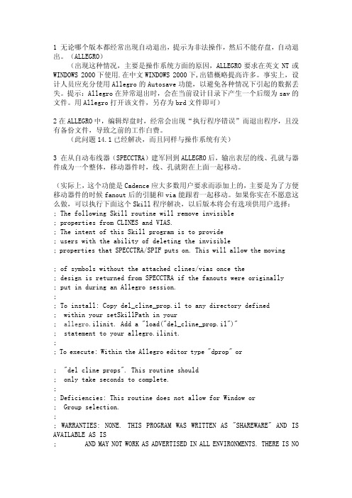
1 无论哪个版本都经常出现自动退出,提示为非法操作,然后不能存盘,自动 退出。(ALLEGRO)
(参考PART2问题7的答案。提示:Allegro在异常退出时,会在当前设计目 录下产生一个后缀为sav的文件。用Allegro打开该文件,另存为brd文件即可)
4 在添加IBIS模型时,MPC8260总是不能自动加上去,已经和工程师联系过多 次。
cadence面试
cadence面试竭诚为您提供优质文档/双击可除cadence面试篇一:微电子一些面试问题亚稳态setup/holdtime是测试芯片对输入信号和时钟信号之间的时间要求。
建立时间是指触发器的时钟信号上升沿到来以前,数据稳定不变的时间。
输入信号应提前时钟上升沿(如上升沿有效)t 时间到达芯片,这个t就是建立时间-setuptime.如不满足setuptime,这个数据就不能被这一时钟打入触发器,只有在下一个时钟上升沿,数据才能被打入触发器。
保持时间是指触发器的时钟信号上升沿到来以后,数据稳定不变的时间。
如果holdtime不够,数据同样不能被打入触发器。
建立时间(setuptime)和保持时间(holdtime)。
建立时间是指在时钟边沿前,数据信号需要保持不变的时间。
保持时间是指时钟跳变边沿后数据信号需要保持不变的时间。
如果不满足建立和保持时间的话,那么dFF将不能正确地采样到数据,将会出现亚稳态(metastability)的情况。
如果数据信号在时钟沿触发前后持续的时间均超过建立和保持时间,那么超过量就分别被称为建立时间裕量和保持时间裕量。
在数字集成电路中,触发器要满足setup/hold的时间要求。
当一个信号被寄存器锁存时,如果信号和时钟之间不满足这个要求,q端的值是不确定的,并且在未知的时刻会固定到高电平或低电平。
这个过程称为亚稳态(metastability)。
一些关于微电子方面的笔试题(zz)1.Fpga和asic的概念,他们的区别。
(未知)Fpga是可编程asic。
asic:专用集成电路,它是面向专门用途的电路,专门为一个用户设计和制造的。
根据一个用户的特定要求,能以低研制成本,短、交货周期供货的全定制,半定制集成电路。
与门阵列等其它asic(applicationspecificic)相比,它们又具有设计开发周期短、设计制造成本低、开发工具先进、标准产品无需测试、质量稳定以及可实时在线检验等优点.2.建立时间是指触发器的时钟信号上升沿到来以前,数据稳定不变的时间。
WCDMA之PA Load-pull 收敛调校
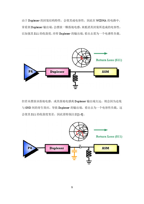
由于Duplexer的封装结构特性,会使其成电容性,因此在WCDMA的电路中,常看到Duplexer输出端,会摆放一颗落地电感,来抵消其封装所造成的电容性,以加强其S11的收敛度,亦即Duplexer的输出端,看出去需为一个电感性负载。
但若未摆放该落地电感,或其落地电感离Duplexer输出端太远,则会因为走线与GND间的寄生效应,导致Duplexer的输出端,看出去为一个电容性负载,这会使其S11的收敛度变差,因此需特别注意[1-3]。
当然原则上,PA输出调试要根据厂家给的Load-pull,去作ACLR,输出功率,耗电流的取舍,但一般方便起见,多半都会调在50奥姆,因为50奥姆在各方面的性能,虽不是最好,但也不至于差到哪去,除非要特别针对某个特性去做优化[4, 6]。
而除非PA输出端有加Isolator,否则从输出端,一路到RF Switch,都算是Load-pull的一部分,因此以[5]的做法,会先量测PA输出端,一直到RF Switch 的Load-pull。
若发现Load-pull不收敛,则会先调校PA输出端的Matching,再调校Duplexer 输出端的Matching。
但因为Duplexer输出端的Matching,同时也会影响接收端的灵敏度,若之前已先调校好接收端的Matching,此时又去动到Duplexer输出端的Matching,则有可能使接收端的灵敏度变差,必须再作微调,以得到最佳灵敏度。
但这么一来,Load-pull又有所变动,如此这样反复调适,有可能会没完没了,因此比较快的做法是反过来,亦即先做Duplexer输出端Matching,确保其S11跟S22,都收敛在50奥姆附近,之后不论要调校发射端或接收端的Matching,这段都不要再更动[6]。
最后再来调适PA的输出Matching,确保从PA输出到Connector,都在50奥姆附近。
值得注意的是,当Connector端接上RF Cable时,其Connector与后面天线弹片间是Open的,此即为最佳的Reference Plane,故理论上可直接将Connector接上RF Cable[4],然而由[7]可知,Connector可能会有来料问题,亦即会有leakage,如下图[8]。
Cadence问答
1 无论哪个版本都经常出现自动退出,提示为非法操作,然后不能存盘,自动退出。
(ALLEGRO)(出现这种情况,主要是操作系统方面的原因,ALLEGRO要求在英文NT或 WINDOWS 2000下使用.在中文WINDOWS 2000下,出错概略提高许多。
事实上,设计人员应充分使用Allegro的Autosave功能,以避免各种情况下引起的数据丢失。
提示:Allegro在异常退出时,会在当前设计目录下产生一个后缀为sav的文件。
用Allegro打开该文件,另存为brd文件即可)2在ALLEGRO中,编辑焊盘时,经常会出现“执行程序错误”而退出程序,且没有备份文件,导致之前的工作白费。
(此问题14.1已经解决,而且同样与操作系统有关)3 在从自动布线器(SPECCTRA)建军回到ALLEGRO后,输出表层的线、孔就与器件成为一个整体,移动器件时,线、孔就附在上面一起移动。
(实际上,这个功能是Cadence应大多数用户要求而添加上的,主要是为了方便移动器件的时候fanout后的引腿和via能跟着一起移动。
如果你实在不愿意这么做,可以执行下面这个Skill程序解决,以后版本将会有选项供用户选择: ; The following Skill routine will remove invisible; properties from CLINES and VIAS.; The intent of this Skill program is to provide; users with the ability of deleting the invisible; properties that SPECCTRA/SPIF puts on. This will allow the moving; of symbols without the attached clines/vias once the; design is returned from SPECCTRA if the fanouts were originally; put in during an Allegro session.;; To install: Copy del_cline_prop.il to any directory defined; within your setSkillPath in your; allegro.ilinit. Add a "load("del_cline_prop.il")"; statement to your allegro.ilinit.;; To execute: Within the Allegro editor type "dprop" or; "del cline props". This routine should; only take seconds to complete.;; Deficiencies: This routine does not allow for Window or; Group selection.;; WARRANTIES: NONE. THIS PROGRAM WAS WRITTEN AS "SHAREWARE" AND IS AVAILABLE AS IS; AND MAY NOT WORK AS ADVERTISED IN ALL ENVIRONMENTS. THERE IS NO; SUPPORT FOR THIS PROGRAM.;; Delete invisible cline/via properties.;axlCmdRegister( "dprop" 'delete_cline_prop)axlCmdRegister( "del cline props" 'delete_cline_prop)(defun delete_cline_prop ();; Set the Find Filter to Select only clines(axlSetFindFilter ?enabled (list "CLINES" "VIAS")onButtons (list "CLINES" "VIAS"));; Select all clines(axlClearSelSet)(axlAddSelectAll) ;select all clines and vias(setq clineSet (axlGetSelSet))(axlDBDeleteProp clineSet "SYMBOL_ETCH") ;Remove the property(axlClearSelSet) ;unselect everything)4.用贴片焊盘(type=single)做成的package,用tools\pads tack\modify design padstack...编辑,发现type变成了blind/buried。
cadence常见技巧和错误。。。
cadence常见技巧和错误。
1.如何在allegro中取消花焊盘(⼗字焊盘)set up->design parameter ->shape->edit global dynamic shape parameters->Thermal relief connects ->Thru pins ,Smd pins -> full contact2.allegro 中如何设置等长setup -> constraints->electrical->net->routing->Min Max Propagation delays选择要等长的net->右击->create->pin pair->选择pin修改 prop daly 的min 和max项3.如何设置allegro的快捷键修改⽂件inst d ir\share\pcb\env或inst_dir\pcbevn\env快捷键定义如下:alias F12 zoom outalias ~R angle 90 (旋转90 度)alias ~F mirror (激活镜相命令)alias ~Z next (执⾏下⼀步命令)alias End redisplay(刷新屏幕)alias Del Delete(激活删除命令)alias Home Zoom fit(全屏显⽰)alias Insert Define grid(设置栅格)alias End redisplayalias Pgdown zoom outalias Pgup zoom inalias F12 custom smoothalias Pgup slidealias Pgdown donealias Home hilightalias End dehilightalias Insert add connectalias Del Delete4.如何在allegro中删除有过孔或布线的层时不影响其他层1.输出specctra的dsn⽂件allegro->file->export->router->demo.dsn->run2.产⽣session⽂件specctra(pcb router)->file->write->session->demo.ses->ok3.删除某⼀层中的布线和过孔delete(ctrl+D)->..4.删除allegro中的板层setup->cross section->⿏标右键->delete5.导⼊session⽂件allegro->file->import->router->demo.ses->run也可先将通过该层的过孔先替换成顶层焊盘,删除该层以后再替换回来5.如何在Allegro中同时旋转多个零件1.Edit->Move 在Options中Rotation的Point选User Pick2 再右键选Term Group 按住⿏标左键不放并拉⼀个框选中器件多余的可⽤Ctrl+⿏标左键点击去掉.3. 选好需整体旋转的器件后右键complete.4. 提⽰你Pick orgion ⿏标左键选旋转中⼼.5 下⾯右键选rotate 即可旋转了.6.allegro 16.0 透明度设置display->colour/visibility->display->OpenGL->Global transparency->transparent7.allegro Drill hole size is equal or larger than smallest pad size.Pad will be drilled away.提⽰Drill hole size is equal or larger than smallest pad size.Pad will be drilled away.不⽤理睬这⼀提⽰8.ALLEGRO 如何⽣成钻孔⽂件Manufacture -> NC -> Drill Customization->auto generate symbolsManufacture -> NC -> Drill LegendManufacture -> NC ->NC parameters->enhanced excellon format->closeManufacture -> NC -> NC Drill->auto tool select->optimize drill head travel9.CAM350如何正确导⼊钻带⽂件导进去后MACRO->PLAY->选择(CAM350--SCRIPTS)PADS_DRILL->选择钻带的REP⽂件还没测试过,rep⽂件从哪⼉来的呢10.allegro 如何设置route keepin,package keepin1.setup->area->route keepin,package keepin ->画框2.edit ->z-copy->options->package keepin,route keepin->offset->50->点击外框11.allegro 中如何禁⽌显⽰shape完全禁⽌的⽅法没找到setup->user preference editor->display->display_shapefill->输⼊⼀个较⼤的数shape在显⽰时就不是那么显眼了set-user preference editor-shape-no shape fill(v)12.如何在allegro设置⾃定义元件库路径在下⾯两个位置添加⾃定义元件的路径Setup->User Preferences Editor->Design_paths->padpathSetup->User Preferences Editor->Design_paths->psmpath1.在allegro中如何修改线宽在Allegro的Setup->constraints⾥的set standard values中可定义每⼀层⾛线的宽度,⽐如,可以定义VCC和GND的线宽为10 Mil。
cadence布线常见问题
1.怎样建立自己的元件库?建立了一个新的project后,画原理图的第一步就是先建立自己所需要的库,所采用的工具就是part developer.首先在建立一个存放元件库的目录(如mylib),然后用写字板打开cds.lib,定义:Define mylib d:boardmylib(目录所在路径).这样就建立了自己的库。
在Concept_HDL的component->add,点击search stack,可以加入该库。
2.保存时Save view和Save all view以及选择Change directory和不选择的区别?建立好一个元件库时,首先要先保存,保存尽量选择save view。
在concept-HDL中,我们用鼠标左键直接点击器件后,便可以对器件的外形尺寸进行修改,这时如果你再进入part developer做一些修改后,如果选择save all view会回到原来的外形尺寸,而选save view 会保留改动后的外形。
3.如何建part库,怎么改变symbol中pin脚的位置?在project manager中tools/part developer可建立,选择库并定义part name,在symbol 中add symbol,package中add package/addpin,依次输入pin:package中:a,Name:pin’s logical name不能重复b,pin:pin的标号,原理图中backannotate后相应的标号c,pin type:pin脚的类型(input,output等,暂可忽略)d,active:pin的触发类型high(高电平),low(低电平)e,nc:填入空脚的标号f,total:此类型的所有pin脚数g,以下暂略symbol中:a,logical name:对应package中的nameb,type:对应package中的typec,position:pin脚在器件中位置(left,right,top,bottom)d,pintext:pin在器件中显示的name(对应package中的pin,但可重复,比如package 中的gnd1和gnd2都可设为gnd)e,active:对应package中的active修改:用part developer打开要修改的器件,*选择edit/restrict changes(若不选择,则器件被保护,修改后存盘无效),一般修改:a,package中相应pin的标号和nameb,pin的active类型c,symbol中各pin脚的顺序(pin脚的顺序在第一次存盘后再次打开会被改变,对于较多pin脚的器件,如232pins,修改较繁琐,故尽力保证的一次的成功率。
Cadence技巧及疑难问题
1.铺平衡铜:命令为:Thieving2.布局布线模块拷贝以下操作均在Placement Edit模式(空白处单击右键-Application Mode-Placement Edit)下。
选中好布局布线完成好的模块,在选中好的模块上单击右键,选用:place replicate create命令Done保存模块文件,以后需要调用选择需要模块重用的模块在选中好的模块上单击右键,选用:place replicate apply 命令下:unnamed选择. ok完成。
3.报错:Design flow is Constraint Manager enabled, require pstcmdb.dat and pstcmbc.dat files。
解决方法:1. In Allegrotype: skill <return>type: axlDBControl('cmgrEnabledFlow nil) <return>.You should see a 't' in the command area which indicates the command was successful.This will reset the branding flag inside the database so netrev will not look for pstcm*.dat files. type: exit <return> to exit the skill interpreterSave the .brd file.2. Delete the 'constraints' folder under <project>/worklib/<design name>3. Delete the 'opf' folder under <project>/worklib/<design name>4. In the 'packaged' directory - delete cmdbview.dat, cmdcview.dat,pstcmdb.dat, pstcmbc.dat, pstcmback.dat5. Run Export Physical to regenerate the netlist files.6. Run Import Logic in Allegro.7. From this point on, constraints are managed in Allegro. Whenever you run Export Logic from Allegro, the checkbox 'Export using Constraint Manager enabled flow' should be unchecked. Important: This procedure assume the design is flat and has been back-annotated。
cadence疑难问题
cadence疑难问题Cadence Troubleshooting GuideA Cadence EDA Tools Help DocumentDocument ContentsIntroductionTroubleshooting GuideIntroductionThis document answers/solutions to common questions/problems encountered using the Cadence EDA tools.Troubleshooting Guide: Frequently Asked QuestionsGeneralMy icfb window is frozen. How do I close it?Open an Xterm window and type ps -u username and note the PID for icfb.exe. Execute the command kill -9 PIDno. This will close the cadence session. Delete the lock files if you have any.How do I open the locked file in edit mode?Go the folder in which your design files are stored. Depending on the number of views your design has, you will have folders named schematic, symbol etc. Go to the folder schematic. You might see the files master.tag pc.db prop.xx sch.cd% sch.cd- sch.cdb sch.cdb.cdslck etc. Leave the files master.tag pc.db prop.xx sch.cdb and delete the other files (using rm filename). After this process you should be able to open the file in edit mode.While doing this you should not have any other cadence session accessing the particular file in edit mode (for example you might be accessing the file from home using Xwin).How do I capture images for my lab report?Refer to the Guide to Capturing Images.Library ManagerWhy can’t I see the default parts libraries in the manager?When you first start Cadence, it creates a new library definition file called “cds.lib” in the directory youlaunched it from. This links the necessary parts libraries to the Cadence workspace. If the file exists in the launch directory but you aren’t seeing the parts libraries, check to make sure that the following line is in“cds.lib”:INCLUDE /opt/cds/local/cdssetup/cds.libIf necessary, add this statement to the “cds.lib” using the text editor of your choice. To avoid having thisproblem in the future, always launch Cadence from your class directory, and try not to edit, move or delete the file unless you need to.Why can’t I see any of my own design libraries in the manager?Most likely, you have launched Cadence from a directory that does not contain all of your previous work. A common mistake is to run icfb from your home directory (“/home//cadence”) and not your class Cadence directory. Make sure you are running icfb from the correct place.Another possibility is that you have copied your design directories to/from another location and the “cds.lib”file that defines the paths to these libraries no longer points to the correct files (or the file is deleted/missing).You will have to manually fix “cds.lib” file by going to Edit->Library Path and enter the library and directory names by hand.Schematic EntryWhy do I get a message "Schematic can't be edited. Do you want to open in Read mode?"Whenever Cadence opens a schematic, it creates a lock file. When you exit the Cadence properly by File -> Exit in the Command Interpreter Window, the lock file will be deleted and you will not have any problems in opening the file in edit mode. If by any chance the session is closed abruptly, the lock files will be in your directory which protects the file to be opened in edit mode.Why is there a yellow X “warning” in open area of my schematic after I do a check?It is likely that you have changed the name of a pin in your schematic after having already designed the symbol for it. You will need to change the name of the pin in either the schematic or symbol so that the two match.Why am I getting a warning for some of the wire crossover points in my circuit after I do a check?By default, Cadence flags the intersection of four wires at a solder dot as a warning. As long as you areconfident that the wire connections are appropriate, then you may ignore these warnings.Symbolic EntryHow do I draw the red selection box around my symbol?Click the “Selection Box” button in the left-hand toolbar of the Symbol Editing window. On the window that pops up, click “Automatic”. This will draw a selection box that bounds the entire symbol within a rectangular selection box.LayoutMy layout is getting bigger and it has some DRC errors, but I couldn't locate them. Is there an easy way to do it?In the layout editor window go to Verify->Markers->Find. In the form, check the option Zoom to markers and click apply. It will zoom in to all the DRC errors.How do I remove the DRC errors markings in my layout, so that I can edit the layout without any dirty white lines?In the layout editor window, go to Verify->Markers->Delete All and say ok to the window that is popping up.This removes all the DRC error markings.When I instantiate my inverter, I can only see a box with the cellname of the inverter. Why is thishappening?This has to do with hierarchical view of the design. When you do the design the topmost cellview (current cellview), it is assigned the number 0 and the other instantiated components are assigned a level above in the hierarchy. The default viewing option is to view the components at a hierarchical level of 0. You can change this by going to Options->Display in the Layout Editor menu and changing the display levels from 0 to 20 (or suitable value of your choice).How do I get the pin names to appear in the layout view?From the menu, select Options->Display. Under display control s, click the box named “Pin Names” on and then click “Apply”.I tried to open a layout and it seems to be invisible. Why can’t I see it?It is possible that no technology library is attached to the cell and that no valid layers are defined (confirm by looking at the LSW window). Attach a tech library to the library where the cell is located by opening the Library manager, right click on the library name, select “Attach T ech Library”, and select theappropriate tech library from the drop-down menu (“AMI 0.60u C5N” for ECE410)Extracted ViewHow do I see the parasitic capacitors in the extracted view?The default setup doesn't extract the parasitic capacitance in the layout. You have to run the command“NCSU_parasiticCapIgnoreThreshold=1e-18” in the command interpreter window before extracting the cell view. Now if you open the extracted view you can see the extracted parasitic capacitors. Press “shift+ f” to see all the transistors in the extracted view.Layout-versus-Schematic (LVS)Why do I get a message that my LVS operation failed?One of the reasons for LVS to fail is that your schematic might not contain a vdd! and gnd! wire. See the output log file for more details. Also, sometimes these LVS failures can be solved by doing the following:1)Open your schematic and save it.2)Open your layout, save it. Pass DRC, and re-extract it3)Open the extracted view and try the LVS once again.The LVS has succeeded, but my netlists fail to match and I don’t understand why.Refer to the Guide to Passing LVS.Analog SimulationHow do I plot signals from nets that are embedded in instances within my schematic?You must descend to the schematic view of the instance that contains the net you wish to plot. Highlight the instance and press “Shift-x” and click “OK”. To return to the top-level schematic, press “b”.I have made a change to my stimulus file, but the waveform results aren’t changing.If you make change to a stimulus file after an initial run of a simulation, it may be necessary to recreate the netlist. This can be done by choosing from the menu Simulation->Netlist->Create Raw. You can close the two netlist windows that pop up, and re-run the simulation.I try to run a simulation, but the waveform results do not appear.There are many reasons this may happen. This may be because:1)You haven’t selected an analysis for simulation, or any outputs to be plotted2)There are errors in your netlist3)You have used a “non-standard” view name (e.g. the view name is “invschematic”). You can check thisfrom viewing the cell name in the Library manager. If the view name is not “schematic”, then it needs to be renamed.4)You made changes to a schematic during simulation, but did not save the schematic. Make sure to save theschematic, and then re-run the simulation.If there are errors in your simulation setup, they are usually reported in the icfb window. Also, it may be possible to view these errors by selecting Simulation -> Output Log. Try to address these errors manually if possible.I try to run a simulation, the waveform results appear, but all of the signals are zero volts.More than likely, your stimulus file is either incorrectly written, incorrectly linked, or missing altogether. Check that the copy of the stimulus file you are working on is the same copy thatyou specified in Affirma Analog environment. A quick way to do this is to close any open copy of the stimulus file, from the menu select Setup ->Stimuli ->Edit Analog. If you enter the name of an existing stimulus file, it should pop in the text editor.I try to run a simulation, the waveform results appear, the inputs are changing correctly, but the outputis not transitioning between Vdd and GND.It is likely that the signal vdd! is not correctly defined. Check your SPICE stimulus file for the line:Vdd vdd! 0 3If you change your stimulus file after an initial simulation, recreate the netlist of your design as described above.I am trying to select an output from my extracted view, but it does not appear as selected in the Analog Design Environment when I click on the nets.Check for the following:1)Make sure the word “extracted” appears before the word “schematic” in the “Switch View List” of theenvironment options.2)Close all extracted views. When you select an output to be plotted, the correct extracted version shouldopen automatically.If this doesn’t help, try the following process:1)Close the Analog Environment.2)Re-extract the layout of the cell.3)Try simulation again.If this doesn’t help, try closing Cadence, re-opening it and running the simulation normally.I have tried EVERYTHING and my simulations still don’t seem to work.Here are some obscure issues that may be causing problems. Consider them only if all of the above suggestions didn’t work:1)If there is white space after any component in your SPICE stimulus file, this can sometimes causeunexpected simulation results. Delete any extra spaces or tabs after each line.2)It is possible that illegal, invisible characters exist between parameter declarations in your stimulus file.Wherever you see a space, try to delete it and re-insert it using the spacebar.3)Add a carriage return (press enter) after the last line in the stimulus file.4)Make sure that no two voltage source names are identical in your stimulus file. This includes caseinsensitive matching for SPICE stimulus files.5)Make sure that all instances in a schematic point to the correct cells. Often, when making copies of cells, orcreating multiple cells with the same name existing in different libraries, you can confuse one for the other and instance the wrong cell in a schematic. You can determine the cell library and name of an instance by selecting and observing its properties by pressing “q”.Cadence software is not without its quirks. If you have tried just about everything and you s till can’t get the correct simulation behavior, try closing and re-launching the analog environment. As second resort, close icfb and re-launch Cadence. As a last resort, log off the computer and log back on, or even switch workstations.This can sometimes fix errors that are too obscure and difficult to identify manually.Stimulus FilesHow do I add comment line in my SPICE file?Adding a * in the first column of the stimulus file comments the line.How do I write stimulus files? How do I specify components in stimulus files?Refer to the Guide to Writing Stimulus Files.How do I “short” two pins together in a stimulus fileThis is done by declaring a 0V DC voltage source with terminal names matching the two pins that need to be shorted. For instance, if you need to short pins A and B together, use the following SPICE code:Vname A B 0(Vname can have any unique name, as long as it starts with “V”).。
Cadence-使用参考手册
Cadence 使用参考手册邓海飞微电子学研究所设计室20XX7月目录概述11.1 Cadence概述11.2 ASIC设计流程1第一章Cadence 使用基础52.1 Cadence 软件的环境设置52.2 Cadence软件的启动方法102.3库文件的管理122.4文件格式的转化132.5 怎样使用在线帮助132.6 本手册的组成14第二章Verilog-XL 的介绍153. 1 环境设置153.2 Verilog-XL的启动153.3 Verilog-XL的界面173.4 Verilog-XL的使用示例183.5 Verilog-XL的有关帮助文件19第四章电路图设计与电路模拟214.1 电路图设计工具Composer (21)4.1.1 设置214.1.2 启动224.1.3 用户界面与使用方法224.1.4 使用示例244.1.5 相关在线帮助文档244.2 电路模拟工具Analog Artist (24)4.2.1 设置244.2.2 启动254.2.3 用户界面与使用方法254.2.5 相关在线帮助文档25第五章自动布局布线275.1 Cadence中的自动布局布线流程275.2 用AutoAbgen进行自动布局布线库设计28第六章版图设计与其验证306.1 版图设计大师Virtuoso Layout Editor (30)6.1.1 设置306.1.2 启动306.1.3 用户界面与使用方法316.1.4 使用示例316.1.5 相关在线帮助文档326.2 版图验证工具Dracula (32)6.2.1 Dracula使用介绍326.2.2 相关在线帮助文档33第七章skill语言程序设计347.1 skill语言概述347.2 skill语言的基本语法347.3 Skill语言的编程环境347.4面向工具的skill语言编程35附录1 技术文件与显示文件示例60附录2 Verilog-XL实例文件721.Test_memory.v (72)2.SRAM256X8.v (73)3.ram_sy1s_8052 (79)4.TSMC库文件84附录3 Dracula 命令文件359概述作为流行的EDA工具之一,Cadence一直以来都受到了广大EDA工程师的青睐。
Cadence常见问题总结
Cadence常见问题总结Cadence常见问题总结一、封装库路径设置Setup →user preferences Editor →Paths →library →Padpath/psmpath设置到库所在位置二、创建焊盘放置pad时报错:cannot be placed outside the drawing extents原因:操作窗口过小,设置大一些Setup →Design Parameters →Design/extents 将变量设大一些三、原理图和Pcb Layout交互运用设置(按模块摆件)在原理图界面,选中.dsn →Options →Preferences/Miscellaneous勾选Enable Intertool Communication(Orcad和Pcb editor 联系的纽带)选中要摆放的模块,拖到layout界面(在layout界面保持Place Manual功能)五,PCB 设计过程中实时查看layout进度Display →Status六、将两个相同属性的shape合在一起Shape →Merge shape →分别点击两个shape七、Via设置成空心的Setup →Design Parameters →Display/勾选Display plated holes八、实时显示走线的长度Setup →user Preferences →Route/Connect/勾选allegro etch length on九、更新部品封装的pad信息打开layout界面,T ools →Padstack →Modify Design Padstack,右侧options 选择要更改的pad →Edit,修改完之后→File →Updateto Design and Exit十、铺铜的两种方式1、shape →polygon, 右侧options里class选etch,sub-class 选择要铺铜的layer,单击鼠标右键→assign net →点击器件的pin →开始画形状2、先画shape,然后选择shape →select shape or void点击sh ape →鼠标右键assign net →点击器件的pin十一、在allegro里把PCB板整个旋转90度选中Move命令,在Options/Point选择User Pick,在Find里全部勾选,右击选中Temp Group,框选整个板子,右击选中Complete,击一点作为User Pick ,然后Rotate十二、对整个原理图重新编号选中.dsn文件→Tools →Annotate →勾选update entire design、Reset part reference to ?(将部品位号全部恢复到?)选中.dsn文件→T ools →Annotate →勾选Refdes control required在右侧相应位置输入起始位号,则可以按page编号十三、allegro 如何设置route keepin,package keepin1、setup →area →route keepin,package keepin →画框2、edit →z-copy →options →package keepin/route keepin →Contract/offset 0.3->点击outline (outline必须是一个封闭的图形)十四、Z-copy失灵首先检查被操作的对象是不是一个封闭的的图形,如果不是,那么就需要把若干segments合成一个整体,shape →compose shape,右侧active class →Board Geometry/outline,框选图中segments,生成shape之后,进行Z-copy,再删掉shape十五、在地平面上加via选择要添加的via →copy,右侧options可以设置via间距和数量十六、快速切换layer设置打开layout界面,Display →Color/Visbility,打开想要显示的内容,View →Color View Save →设置路径,勾选complete →save,将生成文件放到工程allegro目录下即可应用十七、刚安装完软件,手势需要同时按Ctrl+鼠标右键Setup →user preferences Editor →Ui/input →勾选no_dragup →ok经过该设置,画手势只用右键就行十八、设置快捷键Cadence/SPB_16.6/share/pcb/text/env打开env文件(以写字板方式打开)然后进行编辑十九、在原理图赋予器件封装信息双击原理图上元件,弹出对话框,在footprint处输入对应的封装信息,选中Footprint右击Display →勾选value only →apply二十、生成netlist选中.dsn →T ools →create netlist(net名字过长时,系统会自动Rename)如果生成过程中报错,则检查部品封装信息或者device有没有问题。
- 1、下载文档前请自行甄别文档内容的完整性,平台不提供额外的编辑、内容补充、找答案等附加服务。
- 2、"仅部分预览"的文档,不可在线预览部分如存在完整性等问题,可反馈申请退款(可完整预览的文档不适用该条件!)。
- 3、如文档侵犯您的权益,请联系客服反馈,我们会尽快为您处理(人工客服工作时间:9:00-18:30)。
virtuoso 用portadapter拉负载有意义么?
首先是拉得不准的问题因为谐波阻抗没有考虑
第二是拉完之后想用匹配网络实现这个阻抗值但是cadence又没有ADS中的方便的设计匹配的能力
所以我想是不是直接把匹配网络放上去然后扫描元件参数看输出功率这样我觉得更直接一些啊而且在仿真时就已经包括进了对负载谐波阻抗的考虑。
我现在完全是自己
瞎猜。
请问大家什么看法。
谢谢啦
1. 谐波阻抗的问题确实存在,所以确实有一定误差。
不过如果你是class A或AB的话,应该影响不大。
如果是开关功放,load pull的确意义不是那么大了。
2. 用实际电路可以,但是如何去做这样一个二维扫描呢,因为通常来说你至少要3个元件(T或者Pi型),这个你可以思考一下。
load pull实际上就是个二维扫描,你光去扫描C 和L对你的意义不大,看不到smith chart上的各种contour。
非线性pa中的load pull没那么多有用,更不要说谐波的load pull,就算你扫描出来了,匹配电路也没法做。
你已经是非线性pa了,不需要做一个二维的load pull,把Cds估算出来,纳入匹配电路,做一维的电阻扫描就够了。
(其实作为开关型的PA,Cds的非线性也是很大的)
除非你的功率真的很高,>30dBm甚至40dBm,否则load pull稍微偏一点给你带来的功率损失不会超过0.5dB,测试时别的地方带来的不理想造成的误差都比这个影响大。
virtuoso进行loadpull是遇到有portadapter的电阻r为负值
拉负载当输入功率大到一定程度时在所扫描的portadapter的反射系数的所有幅度值中都有portadapter的电阻r为负值这是为啥啊
portadapter内部由L,c,r组成,r和外接的port的z0串联,如果扫描的gamma的模<1,则r+z0>0,-17.8996+50>0,没有任何问题,warning只是提示性的。
关于Cadence下负载牵引的问题
用负载牵引法在Smith原图上仿出等功率圆,如果求最优负载啊,然后如何匹配啊。
资料上说X点就是,在最小圆的圆心,但是为什么我把50欧的电阻匹配到那点后,S21就成负的了啊,
输出功率也很小啊。
请教高人解答。
谢谢
以前搞过,貌似伏在牵引法搞出来的却是不是最优的。
用ADS试试看
要从50欧姆匹配到ZOPT,而不是ZOPT到50,注意方向。
cadence下需匹配后再看功率,否则功率会奇高,因为有负阻,ADS不会有问题。
谢谢楼上回复,方向我没有错,貌似感觉Smith园图上的那个阻抗是归一化的,所以乘上50欧后,貌似效果还行了。
virtuoso中用spectre进行loadpull仿真时出现pss analysis 不收敛的问题
virtuoso中用spectre进行loadpull仿真时
出现pss analysis did not converge的问题可能会出现几次吧但最后也能画出等功率圆。
请问大家这个error是怎么回事?需不需要解决?如何解决?谢谢啦
不收敛就是算不出来按照它说的逐个检查。
output log要仔细看,特别注意每一个warning。
此外,tstab要足够长,以使得电路状态足够稳定。
另外注意不要有悬空的元件。
最后,换换工艺模型,有些fundry的劣质模型容易导致不收敛。