EEPROM I2C操作说明
I2C读写EEPROM文档说明
通过I2C通讯协议对EEPROM进行读写操作发送串口进行通讯一.描述I2CI2C协议有启动,终止,应答,非应答四种信号,有按位发送数据,按位接收数据,有读操作和写操作。
1.启动I2C程序如下,保持SCL为高电平,SDA为高电平,当检测到SDA下降沿时,启动传送,如果2个信号没有被高则返回0。
程序启动成功返回1。
uint8 I2C_Start(void){CyDelayUs(10);SDA_Write(1);CyDelayUs(10);SCL_Write(1);CyDelayUs(10);if ( SDA_Read() == 0) return 0;if ( SCL_Read() == 0) return 0;SDA_Write(0);CyDelayUs(10);SCL_Write(0);CyDelayUs(10);return 1;}上面是模仿I2C启动时序2.终止传送程序如下SDA保持低电平SCL保持高电平而后拉高SDA,系统检测到SDA上升沿则终止传送。
void I2C_Stop(void){CyDelayUs(10);SDA_Write(0);CyDelayUs(10);SCL_Write(1);CyDelayUs(10);SDA_Write(1);CyDelayUs(10);}3.模拟应答信号,让SDA的低电平时间大于SCL的高电平时间,即可应答;也就是SDAvoid I2C_Ack(void){CyDelayUs(10);SDA_Write(0);CyDelayUs(10);SCL_Write(1);CyDelayUs(10);SCL_Write(0);CyDelayUs(10);}4.模拟非应答信号,让SDA的高电平时间大于SCL高电平时间,就是非应答void I2C_Nack(void){CyDelayUs(10);SDA_Write(1);CyDelayUs(10);SCL_Write(1);CyDelayUs(10);SCL_Write(0);CyDelayUs(10);}5.按位发送数据,按位发送数据的要求是数据位高电平的时间大于SCL,SCL高电平时不允许数据位电平变化,只有SCL低电平时才可以任意变换。
CAT24C128 EEPROM 128Kb I2C 说明书
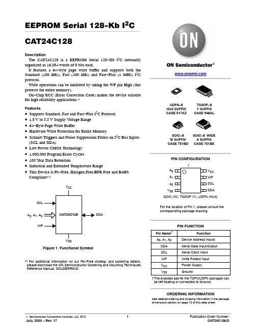
EEPROM Serial 128-Kb I2C CAT24C128DescriptionThe CAT24C128 is a EEPROM Serial 128−Kb I2C internally organized as 16,384 words of 8 bits each.It features a 64−byte page write buffer and supports both the Standard (100 kHz), Fast (400 kHz) and Fast−Plus (1 MHz) I2C protocol.Write operations can be inhibited by taking the WP pin High (this protects the entire memory).On−Chip ECC (Error Correction Code) makes the device suitable for high reliability applications.*Features•Supports Standard, Fast and Fast−Plus I2C Protocol•1.8 V to 5.5 V Supply V oltage Range•64−Byte Page Write Buffer•Hardware Write Protection for Entire Memory•Schmitt Triggers and Noise Suppression Filters on I2C Bus Inputs (SCL and SDA)•Low Power CMOS Technology•1,000,000 Program/Erase Cycles•100 Year Data Retention•Industrial and Extended Temperature Range•This Device is Pb−Free, Halogen Free/BFR Free and RoHS Compliant**Figure 1. Functional Symbol SDASCLWPV CCSSA2, A1, A0** For additional information on our Pb−Free strategy and soldering details,please download the ON Semiconductor Soldering and Mounting Techniques Reference Manual, SOLDERRM/D.PIN CONFIGURATIONSDAWPV CCV SSA2A1A01See detailed ordering and shipping information in the package dimensions section on page 10 of this data sheet.ORDERING INFORMATIONSOIC−8W SUFFIXCASE 751BDSCLSOIC (W), TSSOP (Y), UDFN (HU4)TSSOP−8Y SUFFIXCASE 948ALDevice Address Inputs A0, A1, A2Serial Data Input/OutputSDASerial Clock InputSCLWrite Protect InputWPPower SupplyV CCGroundV SSFunctionPin Name†PIN FUNCTIONFor the location of Pin 1, please consult thecorresponding package drawing.UDFN−8HU4 SUFFIXCASE 517AZ†The exposed pad for the TDFN/UDFN packages canbe left floating or connected to Ground.SOIC−8 WIDEX SUFFIXCASE 751BETable 1. ABSOLUTE MAXIMUM RATINGSParameter Rating Units Storage Temperature−65 to +150°C Voltage on Any Pin with Respect to Ground (Note 1)−0.5 to +6.5V Stresses exceeding those listed in the Maximum Ratings table may damage the device. If any of these limits are exceeded, device functionality should not be assumed, damage may occur and reliability may be affected.1.The DC input voltage on any pin should not be lower than −0.5 V or higher than V CC + 0.5 V. During transitions, the voltage on any pin mayundershoot to no less than −1.5 V or overshoot to no more than V CC + 1.5 V, for periods of less than 20 ns.Table 2. RELIABILITY CHARACTERISTICS (Note 2)Symbol Parameter Min UnitsN END (Notes 3, 4)Endurance1,000,000Program / Erase Cycles T DR Data Retention100Years2.These parameters are tested initially and after a design or process change that affects the parameter according to appropriate AEC−Q100and JEDEC test methods.3.Page Mode, V CC = 5 V, 25°C4.The new product revision (C) uses ECC (Error Correction Code) logic with 6 ECC bits to correct one bit error in 4 data bytes. Therefore, whena single byte has to be written, 4 bytes (including the ECC bits) are re−programmed. It is recommended to write by multiple of 4 bytes in orderto benefit from the maximum number of write cycles.Table 3. D.C. OPERATING CHARACTERISTICS(V CC = 1.8 V to 5.5 V, T A = −40°C to +85°C and V CC = 2.5 V to 5.5 V, T A = −40°C to +125°C, unless otherwise specified.)Symbol Parameter Test Conditions Min Max UnitsI CCR Read Current Read, f SCL = 400 kHz/1 MHz1mAI CCW Write Current3mAI SB Standby Current All I/O Pins at GND or V CC T A = −40°C to +85°C2m AT A = −40°C to +125°C5I L I/O Pin Leakage Pin at GND or V CC T A = −40°C to +85°C1m AT A = −40°C to +125°C2 V IL1Input Low Voltage 2.5 V ≤ V CC≤ 5.5 V−0.50.3 V CC V V IL2Input Low Voltage 1.8 V ≤ V CC < 2.5 V−0.50.25 V CC V V IH1Input High Voltage 2.5 V ≤ V CC≤ 5.5 V0.7 V CC V CC + 0.5V V IH2Input High Voltage 1.8 V ≤ V CC < 2.5 V0.75 V CC V CC + 0.5V V OL1Output Low Voltage V CC≥ 2.5 V, I OL = 3.0 mA0.4V V OL2Output Low Voltage V CC < 2.5 V, I OL = 1.0 mA0.2V Table 4. PIN IMPEDANCE CHARACTERISTICS(V CC = 1.8 V to 5.5 V, T A = −40°C to +85°C and V CC = 2.5 V to 5.5 V, T A = −40°C to +125°C, unless otherwise specified.) Symbol Parameter Conditions Max UnitsC IN (Note 5)SDA I/O Pin Capacitance V IN = 0 V8pFC IN (Note 5)Input Capacitance (other pins)V IN = 0 V6pFI WP, I A (Note 6)WP Input Current, Address InputCurrent (A0, A1, A2)V IN< V IH, V CC = 5.5 V75m A V IN< V IH, V CC = 3.3 V50V IN< V IH, V CC = 1.8 V25V IN> V IH25.These parameters are tested initially and after a design or process change that affects the parameter according to appropriate AEC−Q100and JEDEC test methods.6.When not driven, the WP, A0, A1, A2 pins are pulled down to GND internally. For improved noise immunity, the internal pull−down is relativelystrong; therefore the external driver must be able to supply the pull−down current when attempting to drive the input HIGH. T o conserve power, as the input level exceeds the trip point of the CMOS input buffer (~ 0.5 x V CC), the strong pull−down reverts to a weak current source.Table 5. A.C. CHARACTERISTICS(V CC = 1.8 V to 5.5 V, T A = −40°C to +85°C and V CC = 2.5 V to 5.5 V, T A = −40°C to +125°C)(Note 7)Symbol ParameterStandardV CC = 1.8 V − 5.5 VFastV CC = 1.8 V − 5.5 VFast−Plus (Note 10)V CC = 2.5 V − 5.5 VT A = −405C to +855CUnits Min Max Min Max Min MaxF SCL Clock Frequency1004001,000kHzt HD:STA START Condition Hold Time40.60.25m s t LOW Low Period of SCL Clock 4.7 1.30.45m s t HIGH High Period of SCL Clock40.60.40m s t SU:STA START Condition Setup Time 4.70.60.25m s t HD:DAT Data In Hold Time000m s t SU:DAT Data In Setup Time25010050ns t R (Note 8)SDA and SCL Rise Time1,000300100ns t F (Note 8)SDA and SCL Fall Time300300100ns t SU:STO STOP Condition Setup Time40.60.25m s t BUF Bus Free Time BetweenSTOP and START4.7 1.30.5m st AA SCL Low to Data Out Valid 3.50.90.40m s t DH Data Out Hold Time10010050ns T i (Note 8)Noise Pulse Filtered at SCLand SDA Inputs10010050ns t SU:WP WP Setup Time000m s t HD:WP WP Hold Time 2.5 2.51m s t WR Write Cycle Time555mst PU(Notes 8, 9)Power-up to Ready Mode110.11ms7.Test conditions according to “A.C. Test Conditions” table.8.Tested initially and after a design or process change that affects this parameter.9.t PU is the delay between the time V CC is stable and the device is ready to accept commands.10.Fast−Plus (1 MHz) speed class available for new product revision “C”. The die revision “C” is identified by letter “C” or a dedicated markingcode on top of the package.Table 6. A.C. TEST CONDITIONSInput Levels0.2 x V CC to 0.8 x V CCInput Rise and Fall Times v 50 nsInput Reference Levels0.3 x V CC, 0.7 x V CCOutput Reference Levels0.5 x V CCOutput Load Current Source: I OL = 3 mA (V CC≥ 2.5 V); I OL = 1 mA (V CC < 2.5 V); C L = 100 pFPower−On Reset (POR)The CAT24C128 incorporates Power−On Reset (POR) circuitry which protects the device against powering up in the wrong state.The CAT24C128 will power up into Standby mode after V CC exceeds the POR trigger level and will power down into Reset mode when V CC drops below the POR trigger level. This bi−directional POR feature protects the device against ‘brown−out’ failure following a temporary loss of power. Pin DescriptionSCL: The Serial Clock input pin accepts the Serial Clock generated by the Master.SDA: The Serial Data I/O pin receives input data and transmits data stored in EEPROM. In transmit mode, this pin is open drain. Data is acquired on the positive edge, and is delivered on the negative edge of SCL.A0, A1 and A2: The Address pins accept the device address. When not driven, these pins are pulled LOW internally. WP: The Write Protect input pin inhibits all write operations, when pulled HIGH. When not driven, this pin is pulled LOW internally.Functional DescriptionThe CAT24C128 supports the Inter−Integrated Circuit (I2C) Bus data transmission protocol, which defines a device that sends data to the bus as a transmitter and a device receiving data as a receiver. Data flow is controlled by a Master device, which generates the serial clock and all START and STOP conditions. The CAT24C128 acts as a Slave device. Master and Slave alternate as either transmitter or receiver. Up to 8 devices may be connected to the bus as determined by the device address inputs A0, A1, and A2.I2C Bus ProtocolThe I2C bus consists of two ‘wires’, SCL and SDA. The two wires are connected to the V CC supply via pull−up resistors. Master and Slave devices connect to the 2−wire bus via their respective SCL and SDA pins. The transmitting device pulls down the SDA line to ‘transmit’ a ‘0’ and releases it to ‘transmit’ a ‘1’.Data transfer may be initiated only when the bus is not busy (see A.C. Characteristics).During data transfer, the SDA line must remain stable while the SCL line is HIGH. An SDA transition while SCL is HIGH will be interpreted as a START or STOP condition (Figure 2). The START condition precedes all commands. It consists of a HIGH to LOW transition on SDA while SCL is HIGH. The START acts as a ‘wake−up’ call to all receivers. Absent a START, a Slave will not respond to commands. The STOP condition completes all commands. It consists of a LOW to HIGH transition on SDA while SCL is HIGH.Device AddressingThe Master initiates data transfer by creating a START condition on the bus. The Master then broadcasts an 8−bit serial Slave address. The first 4 bits of the Slave address are set to 1010, for normal Read/Write operations (Figure 3). The next 3 bits, A2, A1 and A0, select one of 8 possible Slave devices and must match the state of the external address pins. The last bit, R/W, specifies whether a Read (1) or Write (0) operation is to be performed.AcknowledgeAfter processing the Slave address, the Slave responds with an acknowledge (ACK) by pulling down the SDA line during the 9th clock cycle (Figure 4). The Slave will also acknowledge all address bytes and every data byte presented in Write mode. In Read mode the Slave shifts out a data byte, and then releases the SDA line during the 9th clock cycle. As long as the Master acknowledges the data, the Slave will continue transmitting. The Master terminates the session by not acknowledging the last data byte (NoACK) and by issuing a STOP condition. Bus timing is illustrated in Figure 5.START CONDITIONSTOP CONDITIONSDASCLFigure 2. START/STOP ConditionsDEVICE ADDRESSFigure 3. Slave Address BitsSCL FROM MASTER≥ t SU:DAT )DATA OUTPUTFROM TRANSMITTERDATA OUTPUT FROM RECEIVERFigure 4. Acknowledge TimingSCLSDA INSDA OUTFigure 5. Bus TimingWrite OperationsByte WriteUpon receiving a Slave address with the R/W bit set to ‘0’,the CA T24C128 will interpret the next two bytes as address bytes. These bytes are used to initialize the internal address counter; the 2 most significant bits are ‘don’t care’, the next 8 point to one of 256 available pages and the last 6 point to a location within a 64 byte page. A byte following the address bytes will be interpreted as data. The data will be loaded into the Page Write Buffer and will eventually be written to memory at the address specified by the 14 active address bits provided earlier. The CAT24C128 will acknowledge the Slave address, address bytes and data byte.The Master then starts the internal Write cycle by issuing a STOP condition (Figure 6). During the internal Write cycle (t WR ), the SDA output will be tri −stated and additional Read or Write requests will be ignored (Figure 7).Page WriteBy continuing to load data into the Page Write Buffer after the 1st data byte and before issuing the STOP condition, up to 64 bytes can be written simultaneously during one internal Write cycle (Figure 8). If more data bytes are loaded than locations available to the end of page, then loading will continue from the beginning of page, i.e. the page address islatched and the address count automatically increments to and then wraps −around at the page boundary. Previously loaded data can thus be overwritten by new data. What is eventually written to memory reflects the latest Page Write Buffer contents. Only data loaded within the most recent Page Write sequence will be written to memory.Acknowledge PollingThe ready/busy status of the CAT24C128 can be ascertained by sending Read or Write requests immediately following the STOP condition that initiated the internal Write cycle. As long as internal Write is in progress, the CAT24C128 will not acknowledge the Slave address.Hardware Write ProtectionWith the WP pin held HIGH, the entire memory is protected against Write operations. If the WP pin is left floating or is grounded, it has no impact on the operation of the CAT24C128. The state of the WP pin is strobed on the last falling edge of SCL immediately preceding the first data byte (Figure 9). If the WP pin is HIGH during the strobe interval, the CA T24C128 will not acknowledge the data byte and the Write request will be rejected.Delivery StateThe CAT24C128 is shipped erased, i.e., all bytes are FFh.SLAVE ADDRESSSA C KA C KA C KS T O P PBUS ACTIVITY:MASTERSLAVES T AR T ADDRESS BYTE ADDRESS BYTE DATA BYTEA C K* = Don’t Care BitFigure 6. Byte Write Sequence**a 13−a 8a 7−a 0STOPCONDITIONSTARTCONDITIONADDRESSSCLSDA Figure 7. Write Cycle TimingSLAVE ADDRESSSA C KA C KC KBUS ACTIVITY:MASTER SLAVEST ARTADDRESS BYTE ADDRESS BYTE DATA BYTE DATA BYTE DATABYTE C KS T O C KC KC K* = Don’t Care Bit P v 63Figure 8. Page Write Sequence**a 13−a 8a 7−a 0ADDRESS BYTEDATA BYTESCLSDA WPFigure 9. WP TimingRead OperationsImmediate ReadUpon receiving a Slave address with the R/W bit set to ‘1’,the CAT24C128 will interpret this as a request for data residing at the current byte address in memory. The CAT24C128 will acknowledge the Slave address, will immediately shift out the data residing at the current address,and will then wait for the Master to respond. If the Master does not acknowledge the data (NoACK) and then follows up with a STOP condition (Figure 10), the CAT24C128returns to Standby mode.Selective ReadTo read data residing at a specific location, the internal address counter must first be initialized as described under Byte Write. If rather than following up the two address byteswith data, the Master instead follows up with an Immediate Read sequence, then the CAT24C128 will use the 14 active address bits to initialize the internal address counter and will shift out data residing at the corresponding location. If the Master does not acknowledge the data (NoACK) and then follows up with a STOP condition (Figure 11), the CAT24C128 returns to Standby mode.Sequential ReadIf during a Read session the Master acknowledges the 1st data byte, then the CAT24C128 will continue transmitting data residing at subsequent locations until the Master responds with a NoACK, followed by a STOP (Figure 12).In contrast to Page Write, during Sequential Read the address count will automatically increment to and then wrap −around at end of memory (rather than end of page).SCL SDA 8th Bit STOPNO ACKDATA OUT8SLAVE ADDRESSSA C KDATA BYTEN O A C K S T O P PS T A R T BUS ACTIVITY:MASTERSLAVEFigure 10. Immediate Read Sequence and Timing9SLAVE ADDRESSSA C KA C K A C K BUS ACTIVITY:MASTERSLAVES T A R T ADDRESS BYTE ADDRESS BYTE DATA BYTESLAVE ADDRESSSA C KP* = Don’t Care BitFigure 11. Selective Read Sequence**S T A R T S T O P A C KN O a 13−a 8a 7−a 0BUS ACTIVITY:MASTERSLAVEBYTE nBYTE n+1BYTE n+2BYTE n+xC KC KC KS T O N O A C C KSLAVE Figure 12. Sequential Read SequenceORDERING INFORMATION(Notes 11 thru 14)Device Order Number SpecificDeviceMarking*PackageType Temperature Range Lead Finish Shipping†CAT24C128WI−GT324128C SOIC−8,JEDECI = Industrial(−40°C to +85°C)NiPdAu Tape & Reel,3,000 Units / ReelCAT24C128YI−GT3C28C TSSOP−8I = Industrial(−40°C to +85°C)NiPdAu Tape & Reel,3,000 Units / ReelCAT24C128HU4IGT3C7U UDFN−8I = Industrial(−40°C to +85°C)NiPdAu Tape & Reel,3,000 Units / Reel†For information on tape and reel specifications, including part orientation and tape sizes, please refer to our Tape and Reel Packaging Specifications Brochure, BRD8011/D.11.All packages are RoHS−compliant (Lead−free, Halogen−free).12.The standard lead finish is NiPdAu.13.For additional package and temperature options, please contact your nearest ON Semiconductor Sales office.14.For detailed information and a breakdown of device nomenclature and numbering systems, please see the ON Semiconductor DeviceNomenclature document, TND310/D, available at ON Semiconductor is licensed by the Philips Corporation to carry the I2C bus protocol.UDFN8, 2x3 EXTENDED PADCASE 517AZ ISSUE ADATE 23 MAR 2015SCALE 2:1NOTES:1.DIMENSIONING AND TOLERANCING PER ASME Y14.5M, 1994.2.CONTROLLING DIMENSION: MILLIMETERS.3.DIMENSION b APPLIES TO PLATEDTERMINAL AND IS MEASURED BETWEEN 0.15 AND 0.25MM FROM THE TERMINAL TIP .4.COPLANARITY APPLIES TO THE EXPOSEDPAD AS WELL AS THE TERMINALS.DIM MIN MAX MILLIMETERS A 0.450.55A10.000.05b 0.200.30D 2.00 BSC D2 1.35 1.45E 3.00 BSC E2 1.25 1.35e 0.50 BSC L 0.250.35*For additional information on our Pb −Free strategy and soldering details, please download the ON Semiconductor Soldering and Mounting Techniques Reference Manual, SOLDERRM/D.SOLDERING FOOTPRINT*DIMENSIONS: MILLIMETERSDETAIL AA30.13 REF L1DETAIL ALALTERNATE CONSTRUCTIONSLL1−−−0.15RECOMMENDEDGENERICMARKING DIAGRAM*XXXXX = Specific Device Code A = Assembly Location WL = Wafer Lot Y = YearW = Work WeekG= Pb −Free Package*This information is generic. Please refer to device data sheet for actual part marking.Pb −Free indicator, “G” or microdot “ G ”,may or may not be present.XXXXX AWLYW G18XDETAIL BALTERNATE CONSTRUCTIONSSOIC −8, 150 mils CASE 751BD ISSUE ODATE 19 DEC 2008IDENTIFICATIONTOP VIEWSIDE VIEWEND VIEWNotes:(1) All dimensions are in millimeters. Angles in degrees.(2) Complies with JEDEC MS-012.SYMBOLMIN NOM MAX θA A1b cD E E1e h 0º8º0.100.330.190.254.805.803.801.27 BSC1.750.250.510.250.505.006.204.00L0.401.271.35TSSOP8, 4.4x3.0, 0.65PCASE 948AL ISSUE ADATE 20 MAY 2022qXXX = Specific Device Code Y = YearWW = Work WeekA = Assembly Location G= Pb −Free Package*This information is generic. Please refer to device data sheet for actual part marking.Pb −Free indicator, “G” or microdot “G ”, may or may not be present. Some products may not follow the Generic Marking.GENERICMARKING DIAGRAM*XXX YWW A GPUBLICATION ORDERING INFORMATIONTECHNICAL SUPPORTLITERATURE FULFILLMENT:。
IIC模拟方式操作EEPROM
{ return 1;//表示无响应 } }while(READ_SDA); SDA_OUT(); I2C_stop (); return 0;//表示操作序列结束 } 简单说明一下: 该函数是用来检测 EEPROM 是否在写数据中,在 AT24C02 数据手册的 P10 中,有一个 响应查询的说明,说到发送起始位,接着发送器件地址,一旦 EEPROM 写数据完成,就会输 出一个低电平。 该函数一个好处是只要 EEPROM 操作完成, 立即在程序中开启写下一个数据, 这明显节省等待时间。 PS:可以用等待 10ms 的延时,测试等待 10ms,对 EEPROM 操作不会有问题。延时小,有问 题的。
i2c总线可以挂载一系列的从设备从设备可以通过地址来区分可是主机如何确保和一个设备通信呢这就得用总线上高低电平来区分了在总线上每个设备使用的是开漏输出硬件保证假设一个从设备拉低总线了那整个sda总线就被拉低了那i2c主机的sda也是低因此这就是所谓的总线所有设备的线与概念简单表示即
IIC 模拟方式操作 EEPROM 介绍
10.I2C 操作 EEPROM 相应的简单函数 a.简单单次写操作,函数 eeprom_write () //针对 EEPROM 编写的写函数 unsigned char eeprom_write(unsigned char c_slave_address7bit,unsigned char c_reg_address,unsigned char u_data) { unsigned char u_wait_err = 0; I2C_start (); I2C_send_byte (c_slave_address7bit << 1); u_wait_err |= I2C_wait_ack (); I2C_send_byte (c_reg_address); u_wait_err |= I2C_wait_ack ();
基于STM32的IIC_EEPROM案例说明

基于STM32的IIC_EEPROM案例说明STM32是一系列由STMicroelectronics开发的32位ARM Cortex-M处理器的微控制器。
它具有高性能、低功耗和丰富的外设。
其中一个外设是I2C接口,可以用于连接外部器件,如EEPROM。
EEPROM(Electrically Erasable Programmable Read-Only Memory)是一种非易失性存储器,可以通过电量抹除并重新编程。
本文将说明如何在STM32微控制器上使用I2C接口来读取和写入EEPROM的数据。
以下是一个I2CEEPROM案例的步骤:1.硬件连接:找到适当的引脚连接STM32和EEPROM。
根据STM32型号和EEPROM的规格书,将SCL引脚连接到STM32的相应引脚,将SDA引脚连接到STM32的相应引脚。
确保EEPROM上的地址引脚正确连接到STM32的引脚,以选择EEPROM的地址。
另外,确保STM32的引脚配置正确。
2.初始化I2C外设:在STM32的代码中,首先需要初始化I2C外设。
这可以通过配置I2C控制器的寄存器来完成。
这些寄存器包含有关时钟速度、地址模式和使能I2C控制器的设置选项。
3.选择EEPROM地址:通过向I2C总线发送一个特定的命令字节,可以选择EEPROM的地址。
这个命令字节包含I2C总线上的设备地址和寻址模式。
4.读取EEPROM数据:为了从EEPROM读取数据,STM32将发送一个读取命令字节,将该命令字节传送到EEPROM,然后从EEPROM读取数据。
在读取数据之前,需要设置读取数据的长度和目标缓冲区。
5.写入EEPROM数据:为了向EEPROM写入数据,STM32将发送一个写入命令字节,将该命令字节传送到EEPROM,然后将数据写入EEPROM。
在写入数据之前,需要设置写入数据的长度和源缓冲区。
6.处理错误和超时:在进行I2CEEPROM读取和写入操作时,可能会出现错误和超时。
二线制I2C CMOS 串行EEPROM 读写操作

reg[10:0]main_state;//主状态寄存器
reg[7:0]data_from_rm;//EEPROM读寄存器
reglink_sda;//SDA数据输入EEPROM开关
reglink_read;//EEPROM读寄存器开关
reglink_head;//启动信号开关
sh8in_bit6= 10'b0000000100,
sh8in_bit5= 10'b0000001000,
sh8in_bit4= 10'b0000010000,
sh8in_bit3= 10'b0000100000,
sh8in_bit2= 10'b0001000000,
sh8in_bit1= 10'b0010000000,
sh8out_end= 9'b100000000;
////////////串行数据并行输出状态定义///////////////////////////////////////////////////
parameter
sh8in_begin= 10'b0000000001,
sh8in_bit7= 10'b0000000010,
// //synthesis parallel_case //case语句综合为并行多路选择器
// //synthesis full_case //case语句分支项完备
// //synthesis translate_on //开始综合以下内容
// //synthesis translate_off //停止综合以下内容,以下内容仅供仿真
main_state<= READ_START;
STC单片机EEPROM读写程序
STC单片机EEPROM读写程序在单片机中,EEPROM(Electrically Erasable Programmable Read-Only Memory)是一种非易失性存储器,可以用于存储数据,即使在断电情况下,数据也会被保留。
因此,掌握STC单片机的EEPROM读写程序对于开发嵌入式系统非常重要。
一、EEPROM简介EEPROM是一种可重复擦写的存储器,可用于存储小量数据。
与Flash存储器相比,EEPROM具有更快的写入和擦除速度。
在STC单片机中,EEPROM的存储容量通常较小,一般在几个字节到几千字节之间。
二、EEPROM读操作在STC单片机中,进行EEPROM读操作需要按照以下步骤进行:1. 初始化I2C总线:STC单片机使用I2C总线进行EEPROM读写操作,因此需要先初始化I2C总线。
通过设置相关寄存器,设置I2C 总线的速度和地址。
2. 发送设备地址:确定要读取的EEPROM设备的地址,并发送到I2C总线。
3. 发送寄存器地址:确定要读取的EEPROM寄存器地址,并将其发送到I2C总线。
4. 发送读命令:向EEPROM发送读命令,以启动读操作。
5. 读取数据:从EEPROM中读取数据,并保存到变量中。
6. 结束读操作:完成读操作后,关闭I2C总线。
三、EEPROM写操作类似于读操作,进行EEPROM写操作也需要按照一定的步骤进行:1. 初始化I2C总线:同样地,首先需要初始化I2C总线。
2. 发送设备地址:确定要写入的EEPROM设备的地址,并发送到I2C总线。
3. 发送寄存器地址:确定要写入的EEPROM寄存器地址,并将其发送到I2C总线。
4. 发送写命令:向EEPROM发送写命令,以启动写操作。
5. 写入数据:将要写入EEPROM的数据发送到I2C总线。
6. 结束写操作:完成写操作后,关闭I2C总线。
四、注意事项在进行EEPROM读写操作时,需要注意以下几点:1. 确保正确的设备地址:要与EEPROM的地址匹配,否则无法进行有效的读写操作。
eeprom i2c C51程序
/*本程序是用eeprom A T24C02保存数码管显示秒时间数据。
*/#include <reg52.h>#include <intrins.h>sbit scl=P3^7; //I2C时钟线sbit sda=P3^6; //I2C数据线bit write=0;unsigned char code ledmap[]={0xc0,0xf9,0xa4,0xb0,0x99,0x92,0x82,0xf8,0x80,0x90,0xff}; //共阴极编码unsigned char num,sec,ledbuf[6];void delay(unsigned int z ){unsigned char i; //显示用的延时程序while(--z)for(i=110;i>0;i++);}void delayus(void){;;}void initi2c(void){sda=1;delayus(); //I2C初始化scl=1;delayus();}void i2cstart(void){sda=1;delayus(); //i2c起始信号scl=1;delayus();sda=0;delayus();}void ack(){unsigned char i;scl=1;i=0; //i2c的应答信号delayus();while((sda==1)&&(i<255))i++;scl=0;}void i2cstop(void){sda=0;delayus();scl=1; //i2c的停止信号delayus();sda=1;delayus();}void i2csend(unsigned char byte){unsigned char mask,i;mask=byte;for(i=0;i<8;i++) //I2C发送一个字节数据{mask=mask<<1; //从最高位开始传送scl=0; //按照I2C的协议传送数据时,SCL边低delayus();sda=CY; //传送delayus();scl=1;delayus();}scl=0;delayus(); //传送完后,scl变低sda=1; //传送完毕后拉高数据线delayus();}unsigned char i2cread(void){unsigned char byte,i;scl=0;delayus();sda=1;delayus(); //接收8位数据子程序for(i=0;i<8;i++){//读一个字节scl=1; //读的时候SCL为高,稳定数据byte<<=1;byte|=sda;scl=0;delayus();}return byte;}unsigned char read_eeprom(unsigned char addr){unsigned char databyte; //读取EEPROM数据函数i2cstart(); //发起始信号i2csend(0xa0); //发器件写地址ack(); //应答i2csend(addr); //发器件子地址ack(); //应答i2cstart(); //发起始信号i2csend(0xa1); //发器件读地址ack(); //应答databyte=i2cread(); //读器件子地址数据i2cstop(); //停止return databyte;}void write_eeprom(unsigned char addr,unsigned char databyte) {i2cstart();i2csend(0xa0);ack(); //向i2c 的eeprom写数据i2csend(addr);ack();i2csend(databyte);ack();i2cstop();}void disp(){unsigned char pos,j; //秒显示子程序pos=0x08;for(j=0;j<6;j++){P1=0x00;P0=ledbuf[j];P1=pos;delay(1);pos++;}P1=0x00;}void t0int() interrupt 1{TH0=0x4c; //由于是11.0592的晶振,定时器定时50ms TL0=0x00;num++;if(num==20) //20次就是一秒钟{num=0;sec++; //秒加一write=1; //此时把秒写进I2C进去,另write标志为一if(sec==100) //显示100秒为此sec=0;}}void main(){initi2c(); //I2C初始化sec=read_eeprom(0); //将I2C地址0的数据写进秒数据里if(sec>100)sec=0;num=0;TMOD=0x01; //定时器0方式1TH0=0x4c; //初始化TL0=0x00;IE=0x82; //定时器总中断为1,ET0=1TR0=1; //开始定时while(1){ledbuf[0]=ledmap[sec%10]; //显示在6个数码管开始2位ledbuf[1]=ledmap[sec/10];ledbuf[2]=0xff; //高四位不显示ledbuf[3]=0xff;ledbuf[4]=0xff;ledbuf[5]=0xff;disp();if(write==1){write=0; //如果为1则将秒数据写进eeprom里write_eeprom(0,sec);}}}。
STM32F4利用I2C向EEPROM写入、读取数据步骤
STM32F4利⽤I2C向EEPROM写⼊、读取数据步骤
写⼊⼀个字节:
第⼀步:使⽤库函数I2C_GenerateSTART()产⽣I2C起始信号,调⽤库函数I2C_CheckEvent()检测事件,若检测到下⼀事件,则进⼊通讯下⼀阶段
第⼆步:调⽤库函数I2C_Send7bitAddress()发送EEPROM的设备地址,并把数据传输⽅向设置为I2C_Direction_Transmitter(即发送⽅向),发送地址后以同样的⽅式检测相应的事件。
第三步:调⽤库函数I2C_SendData向EEPROM发送要写⼊的地址,发送完后等待EV8事件的产⽣。
第四步:继续调⽤库函数I2C_SendData向EEPROM发送要写⼊的数据,然后等待EV8事件的产⽣。
第五步:通讯结束,调⽤I2C_GenerateSTOP发送停⽌信号。
读取⼀字节的数据:
第⼀步:通过库函数I2C_GETFlagStatus()查询库函数是否处于忙碌状态,若不忙碌,则进⼊下⼀状态。
第⼆步:使⽤库函数I2C_GenerateSTART()产⽣起始信号,调⽤库函数I2C_CheckEvent()检测Event1,若检测成功则进⼊下⼀阶段。
第三步:发送EEPROM的设备地址,⽅向为I2C_Direction_Transmitter(即写⽅向),检测事件6
第四步:利⽤库函数I2C_Cmd重新使能I2C外设
第五步:利⽤库函数I2C_Senddata()发送要读取的EEPROM的内部地址,检测Event8事件的产⽣
第六步:产⽣第⼆次I2C起始信号,并检测相关事件
第七步:发送I2C设备地址
第⼋步:读取数据。
EEPROMI2C操作说明
EEPROMI2C操作说明EEPROM (Electrically Erasable Programmable Read-Only Memory)是一种非易失性存储器,可以通过电子方式擦除和编程,同时可以通过I2C总线进行操作。
本文将详细介绍EEPROM的I2C操作说明。
I2C(Inter-Integrated Circuit)是一种串行通信接口协议,可以在多个设备之间进行通信。
在EEPROM的I2C操作中,需要了解以下几个重要的概念和步骤。
1.设备地址:每个通过I2C连接的设备都有一个唯一的设备地址。
在EEPROM的I2C操作中,需要使用设备地址来与EEPROM进行通信。
2.起始条件和停止条件:I2C通信中,起始条件表示通信的开始,停止条件表示通信的结束。
起始条件由一个高电平到低电平的SCL上升沿和一个低电平的SDA下降沿组成,停止条件由一个低电平到高电平的SCL上升沿和一个高电平的SDA上升沿组成。
3. 数据传输:I2C通信中,数据可以以字节的形式进行传输。
每个字节由8个bit组成,包括7个数据位和1个校验位。
在进行EEPROM的I2C操作时,通常需要经过以下几个步骤:1.发送起始条件:将SCL和SDA引脚拉高,然后将SDA引脚拉低,形成起始条件。
2.发送设备地址和写命令:根据EEPROM的设备地址,将设备地址和写命令(0)发送到SDA引脚。
3.发送要写入的地址:将要写入数据的地址发送到SDA引脚。
4.发送数据:将要写入的数据发送到SDA引脚。
5.发送停止条件:将SCL引脚拉高,然后将SDA引脚拉高,形成停止条件。
实际的EEPROM的I2C操作可能还包括以下一些操作:1.读操作:通过发送读命令(1)和读取数据的地址,可以从EEPROM 中读取数据。
读操作与写操作类似,只是需要在发送设备地址时,将写命令(0)改为读命令(1)。
2.擦除操作:EEPROM的主要特点之一是可以擦除数据。
通过发送擦除命令和要擦除的数据的地址,可以将指定数据段擦除为初始值。
EEPROM I2C操作说明知识讲解
E E P R O M I2C操作说明I2C协议2条双向串行线,一条数据线SDA,一条时钟线SCL。
SDA传输数据是大端传输,每次传输8bit,即一字节。
支持多主控(multimastering),任何时间点只能有一个主控。
总线上每个设备都有自己的一个addr,共7个bit,广播地址全0.系统中可能有多个同种芯片,为此addr分为固定部分和可编程部份,细节视芯片而定,看datasheet。
1.1 I2C位传输数据传输:SCL为高电平时,SDA线若保持稳定,那么SDA上是在传输数据bit;若SDA发生跳变,则用来表示一个会话的开始或结束(后面讲)数据改变:SCL为低电平时,SDA线才能改变传输的bit1.2 I2C开始和结束信号开始信号:SCL为高电平时,SDA由高电平向低电平跳变,开始传送数据。
结束信号:SCL为高电平时,SDA由低电平向高电平跳变,结束传送数据。
1.3 I2C应答信号Master每发送完8bit数据后等待Slave的ACK。
即在第9个clock,若从IC发ACK,SDA会被拉低。
若没有ACK,SDA会被置高,这会引起Master发生RESTART或STOP流程,如下所示:1.4 I2C写流程写寄存器的标准流程为:1. Master发起START2. Master发送I2C addr(7bit)和w操作0(1bit),等待ACK3. Slave发送ACK4. Master发送reg addr(8bit),等待ACK5. Slave发送ACK6. Master发送data(8bit),即要写入寄存器中的数据,等待ACK7. Slave发送ACK8. 第6步和第7步可以重复多次,即顺序写多个寄存器9. Master发起STOP写一个寄存器写多个寄存器1.5 I2C读流程读寄存器的标准流程为:1. Master发送I2C addr(7bit)和w操作1(1bit),等待ACK2. Slave发送ACK3. Master发送reg addr(8bit),等待ACK4. Slave发送ACK5. Master发起START6. Master发送I2C addr(7bit)和r操作1(1bit),等待ACK7. Slave发送ACK8. Slave发送data(8bit),即寄存器里的值9. Master发送ACK10. 第8步和第9步可以重复多次,即顺序读多个寄存器读一个寄存器读多个寄存器1.前言对于大多数工程师而言,I2C永远是一个头疼的问题。
- 1、下载文档前请自行甄别文档内容的完整性,平台不提供额外的编辑、内容补充、找答案等附加服务。
- 2、"仅部分预览"的文档,不可在线预览部分如存在完整性等问题,可反馈申请退款(可完整预览的文档不适用该条件!)。
- 3、如文档侵犯您的权益,请联系客服反馈,我们会尽快为您处理(人工客服工作时间:9:00-18:30)。
I2C协议2条双向串行线,一条数据线SDA,一条时钟线SCL。
SDA传输数据是大端传输,每次传输8bit,即一字节。
支持多主控(multimastering),任何时间点只能有一个主控。
总线上每个设备都有自己的一个addr,共7个bit,广播地址全0.系统中可能有多个同种芯片,为此addr分为固定部分和可编程部份,细节视芯片而定,看datasheet。
1.1 I2C位传输数据传输:SCL为高电平时,SDA线若保持稳定,那么SDA上是在传输数据bit;若SDA发生跳变,则用来表示一个会话的开始或结束(后面讲)数据改变:SCL为低电平时,SDA线才能改变传输的bit1.2 I2C开始和结束信号开始信号:SCL为高电平时,SDA由高电平向低电平跳变,开始传送数据。
结束信号:SCL为高电平时,SDA由低电平向高电平跳变,结束传送数据。
1.3 I2C应答信号Master每发送完8bit数据后等待Slave的ACK。
即在第9个clock,若从IC发ACK,SDA会被拉低。
若没有ACK,SDA会被置高,这会引起Master发生RESTART或STOP流程,如下所示:1.4 I2C写流程写寄存器的标准流程为:1. Master发起START2. Master发送I2C addr(7bit)和w操作0(1bit),等待ACK3. Slave发送ACK4. Master发送reg addr(8bit),等待ACK5. Slave发送ACK6. Master发送data(8bit),即要写入寄存器中的数据,等待ACK7. Slave发送ACK8. 第6步和第7步可以重复多次,即顺序写多个寄存器9. Master发起STOP写一个寄存器写多个寄存器1.5 I2C读流程读寄存器的标准流程为:1. Master发送I2C addr(7bit)和w操作1(1bit),等待ACK2. Slave发送ACK3. Master发送reg addr(8bit),等待ACK4. Slave发送ACK5. Master发起START6. Master发送I2C addr(7bit)和r操作1(1bit),等待ACK7. Slave发送ACK8. Slave发送data(8bit),即寄存器里的值9. Master发送ACK10. 第8步和第9步可以重复多次,即顺序读多个寄存器读一个寄存器读多个寄存器1.前言对于大多数工程师而言,I2C永远是一个头疼的问题。
相比UART和SPI而言,I2C的时序要复杂一些,I2C组合变化也丰富一些。
在这里以AT24C04为例说明I2C使用过程中的一些注意点。
2.AT24C04操作示意图图AT24C04操作示意图示意图说明:示意图分阐述了4种不同的操作方式,例如写单个存储单元,写多个存储单元,读单个存储单元和写单个存储单元。
对于单个操作而言,上部为MCU通过I2C输出的相关指令,下部为I2C设备的响应。
例如写单个存储单元操作时,MCU发出I2C启动,设备地址,写标志位等,而I2C设备输出多个ACK。
3.若干说明3.1 基本操作方式I2C设备的操作可分为写单个存储字节,写多个存储字节,读单个存储字节和读多个存储字节。
相对于AT24C04而言,这些读写动作相对于内部的存储单元而言,对于其他的具备I2C接口的AD或传感器而言,存储单元变成了寄存器单元。
虽然存在概念上的差别,但是其操作原理确实一样的。
3.2 无应答在以上4种情况中,无应答为MCU发出,无应答意为MCU不需要从机输出数据,MCU将会停止本次I2C操作。
需要说明的是,无应答并不是一种异常情况。
3.3 I2C设备并不只有一个设备地址这一点往往被忽略,一般情况下认为在I2C启动信号之后的字节为I2C从机地址(7位)。
对于AT24C04而言,内部具有4Kb存储位,合计512字节。
若需要访问512字节内容,总共需要9根地址线(8位宽度),那么上图中的存储地址(8位长度)显然还差了一位,那么就需要从设备地址中“借”1位,这就使得AT24C04具有两个I2C地址,例如0x50和0x51。
3.4 存储地址相对于AT24C04而言,存储地址占1个字节。
若换成其他I2C设备,例如ADXL345,存储地址被寄存器地址替代即可,其他操作方式相似。
但是像AT24C32或AT24C64这样的大容量EEPROM,则存储地址需要2字节描述,也就意味着需要连续发送两个字节地址信息且高字节在前。
其他像BH1750这样的光照芯片,存储地址被具体的操作命令替代,使用I2C设备时需要因地制宜,切不可照搬教条。
3.5 连续读和连续写限制AT24C04中存在页的概念,一页的大小为8字节,若果在单页的范围内,存储地址累加,若超过该页的最大地址,存储地址回到页开始处。
所以对于连续读和连续写而言,最大的操作字节数为8。
若需要操作的字节内容超过8字节,则需要进行翻页操作,即写入下一页的起始存储地址。
4 总结I2C设备有很多种,若掌握基本原理,便可见招拆招,那是I2C总线就不那么难了。
5.参考资料2. PowerPC的I2C实现Mpc8560的CCSR中控制I2C的寄存器共有6个。
2.1 I2CADR 地址寄存器CPU也可以是I2C的Slave,CPU的I2C地址有 I2CADR指定2.2 I2CFDR 频率设置寄存器The serial bit clock frequency of SCL is equal to the CCB clock divided by the divider.用来设置I2C总线频率2.3 I2CCR 控制寄存器MEN: Module Enable. 置1时,I2C模块使能MIEN:Module Interrupt Enable. 置1时,I2C中断使能。
MSTA:Master/slave mode. 1 Master mode,0 Slave mode.当1->0时,CPU发起STOP信号当0->1时,CPU发起START信号MTX:Transmit/receive mode select.0 Receive mode,1 Transmit mode TXAK:Transfer acknowledge. 置1时,CPU在9th clock发送ACK拉低SDA RSTA:Repeat START. 置1时,CPU发送REPEAT STARTBCST:置1,CPU接收广播信息(信息的slave addr为7个0)2.4 I2CSR 状态寄存器MCF:0 Byte transfer is in process1 Byte transfer is completedMAAS:当CPU作为Slave时,若I2CDR与会话中Slaveaddr匹配,此bit被置1MBB:0 I2C bus idle1 I2C bus busyMAL:若置1,表示仲裁失败BCSTM:若置1,表示接收到广播信息SRW:When MAAS is set, SRW indicates the value of the R/W command bit of the calling address, which is sent from the master.0 Slave receive, master writing to slave1 Slave transmit, master reading from slaveMIF:Module interrupt. The MIF bit is set when an interrupt is pending, causing a processor interrupt request(provided I2CCR[MIEN] is set)RXAK:若置1,表示收到了ACK2.5 I2CDR 数据寄存器这个寄存器储存CPU将要传输的数据。
3. PPC-Linux中I2C的实现内核代码(linux-2.6.24)中,通过I2C总线存取寄存器的函数都在文件drivers/i2c/busses/i2c-mpc.c中最重要的函数是mpc_xfer.1.static int mpc_xfer(struct i2c_adapter *adap,struct i2c_msg *msgs,int num)2.{3.struct i2c_msg *pmsg;4.int i;5.int ret = 0;6.unsigned long orig_jiffies = jiffies;7.struct mpc_i2c *i2c = i2c_get_adapdata(adap);8.9. mpc_i2c_start(i2c);// 设置I2CCR[MEN], 使能I2C module10.11./* Allow bus up to 1s to become not busy */12.//一直读I2CSR[MBB],等待I2C总线空闲下来13.while(readb(i2c->base + MPC_I2C_SR)& CSR_MBB){14.if(signal_pending(current)){15. pr_debug("I2C: Interrupted\n");16. writeccr(i2c, 0);17.return-EINTR;18.}19.if(time_after(jiffies, orig_jiffies + HZ)){20. pr_debug("I2C: timeout\n");21.if(readb(i2c->base + MPC_I2C_SR)==22.(CSR_MCF | CSR_MBB | CSR_RXAK))23. mpc_i2c_fixup(i2c);24.return-EIO;25.}26. schedule();27.}28.29.for(i = 0; ret >= 0 && i < num; i++){30. pmsg =&msgs[i];31. pr_debug("Doing %s %d bytes to 0x%02x - %d of %d messages\n",32. pmsg->flags & I2C_M_RD ?"read":"write",33. pmsg->len, pmsg->addr, i + 1, num);34.//根据消息里的flag进行读操作或写操作35.if(pmsg->flags & I2C_M_RD)36. ret = mpc_read(i2c, pmsg->addr, pmsg->buf, pmsg->len, i);37.else38. ret = mpc_write(i2c, pmsg->addr, pmsg->buf, pmsg->len, i);39.}40. mpc_i2c_stop(i2c);//保证为I2CCSR[MSTA]为0,保证能触发STOP41.return(ret < 0)? ret : num;42.}1.static int mpc_write(struct mpc_i2c *i2c,int target,2.const u8 * data,int length,int restart)3.{4.int i;5.unsigned timeout = i2c->adap.timeout;6. u32 flags = restart ? CCR_RSTA : 0;7.8./* Start with MEN *///以防万一,保证I2C模块使能起来9.if(!restart)10. writeccr(i2c, CCR_MEN);11./* Start as master *///写了I2CCR[CCR_MSTA],触发CPU发起START信号12. writeccr(i2c, CCR_MIEN | CCR_MEN | CCR_MSTA | CCR_MTX | flags);13./* Write target byte *///CPU发送一个字节,slave I2C addr和0 (写操作bit)14. writeb((target << 1), i2c->base + MPC_I2C_DR);15.16.if(i2c_wait(i2c, timeout, 1)< 0)//等待slave 发ACK17.return-1;18.19.for(i = 0; i < length; i++){20./* Write data byte */21. writeb(data[i], i2c->base + MPC_I2C_DR);//CPU接着发数据,包括reg addr和data22.23.if(i2c_wait(i2c, timeout, 1)< 0)//等待slave 发ACK24.return-1;25.}26.27.return 0;28.}1.static int i2c_wait(struct mpc_i2c *i2c,unsigned timeout,int writing)2.{3.unsigned long orig_jiffies = jiffies;4. u32 x;5.int result = 0;6.7.if(i2c->irq == 0)8.{//循环读I2CSR,直到I2CSR[MIF]置19.while(!(readb(i2c->base + MPC_I2C_SR)& CSR_MIF)){10. schedule();11.if(time_after(jiffies, orig_jiffies + timeout)){12. pr_debug("I2C: timeout\n");13. writeccr(i2c, 0);14. result =-EIO;15.break;16.}17.}18. x = readb(i2c->base + MPC_I2C_SR);19. writeb(0, i2c->base + MPC_I2C_SR);20.}else{21./* Interrupt mode */22. result = wait_event_interruptible_timeout(i2c->queue,23.(i2c->interrupt & CSR_MIF), timeout * HZ);24.25.if(unlikely(result < 0)){26. pr_debug("I2C: wait interrupted\n");27. writeccr(i2c, 0);28.}else if(unlikely(!(i2c->interrupt & CSR_MIF))){29. pr_debug("I2C: wait timeout\n");30. writeccr(i2c, 0);31. result =-ETIMEDOUT;32.}33.34. x = i2c->interrupt;35. i2c->interrupt = 0;36.}37.38.if(result < 0)39.return result;40.41.if(!(x & CSR_MCF)){42. pr_debug("I2C: unfinished\n");43.return-EIO;44.}45.46.if(x & CSR_MAL){//仲裁失败47. pr_debug("I2C: MAL\n");48.return-EIO;49.}50.51.if(writing &&(x & CSR_RXAK)){//写后没收到ACK52. pr_debug("I2C: No RXAK\n");53./* generate stop */54. writeccr(i2c, CCR_MEN);55.return-EIO;56.}57.return 0;58.}1.static int mpc_read(struct mpc_i2c *i2c,int target,2. u8 * data,int length,int restart)3.{4.unsigned timeout = i2c->adap.timeout;5.int i;6. u32 flags = restart ? CCR_RSTA : 0;8./* Start with MEN *///以防万一,保证I2C模块使能9.if(!restart)10. writeccr(i2c, CCR_MEN);11./* Switch to read - restart */12. //注意这里,再次把CCR_MSTA置1,再触发 START13. writeccr(i2c, CCR_MIEN | CCR_MEN | CCR_MSTA | CCR_MTX | flags);14.15.16./* Write target address byte - this time with the read flag set */17.//CPU发送slave I2C addr和读操作118. writeb((target << 1)| 1, i2c->base + MPC_I2C_DR);//等待Slave发ACK1.if(i2c_wait(i2c, timeout, 1)< 0)2.return-1;3.4.if(length){5.if(length == 1)6. writeccr(i2c, CCR_MIEN | CCR_MEN | CCR_MSTA | CCR_TXAK);7.else//为什么不置 TXAK8. writeccr(i2c, CCR_MIEN | CCR_MEN | CCR_MSTA);9./* Dummy read */10. readb(i2c->base + MPC_I2C_DR);11.}12.13.for(i = 0; i < length; i++){14.if(i2c_wait(i2c, timeout, 0)< 0)15.return-1;16.17./* Generate txack on next to last byte */18.//注意这里TXAK置1,表示CPU每收到1byte数据后,会发送ACK19.if(i == length - 2)20. writeccr(i2c, CCR_MIEN | CCR_MEN | CCR_MSTA | CCR_TXAK);21.22./* Generate stop on last byte */23.//注意这里CCR_MSTA [1->0] CPU会触发STOP24.if(i == length - 1)25. writeccr(i2c, CCR_MIEN | CCR_MEN | CCR_TXAK);26.27. data[i]= readb(i2c->base + MPC_I2C_DR);28.}30.return length;31.}。