EM3_V3.0原理图(2015_05_15)
ESP32 Chip Revision v3.0 用户指南说明书

ESP32 Chip Revision v3.0 User GuideVersion 1.3Espressif SystemsCopyright © 2022About This GuideThis document describes differences between chip revision v3.0 and previous ESP32 chiprevisions.Release NotesDocumentation Change NotificationEspressif provides email notifications to keep customers updated on changes totechnical documentation. Please subscribe at https:///en/subscribe .CertificationDownload certificates for Espressif products from https:///en/certificates . DateVersion Release notes 2020.01V1.0Initial release.2020.07V1.1Added item 6 to Chapter 1 Design Changes in ECO V3.2022.10v1.2Replaced “ECO” with “Chip Revision” Renamed this document as “ESP32 Chip Revision v3.0 User Guide”2022.11v1.3Added item 1 to Chapter 1 Design Changes in ECO V3.Table of Contents................................................................................. 1.Design Changes in Chip Revision v3.0 1............................................................................................... 2.Impact on Customer Projects 2..........................................................................e Case 1: Hardware and Software Upgrade 2........................................................................................e Case 2: Hardware Upgrade Only 2................................................................................................................ bel Specification 3............................................................................................................. 4.Ordering Information 41. Design Changes in Chip Revision v3.0 1.Design Changes in ChipRevision v3.0Espressif has released ESP32 chip revision v3.0 that features wafer-level changes basingon previous ESP32 chip revisions. The design changes introduced on the ESP32 chiprevision v3.0 are:1.Fixed "Due to the flash start-up time, a spurious watchdog reset occurs when ESP32 ispowered up or wakes up from Deep-sleep". Details of the issue can be found in item 3.8in ESP32 Series SoC Errata.2.PSRAM Cache Bug Fix: Fixed “When the CPU accesses the external SRAM in a certainsequence, read & write errors can occur”. Details of the issue can be found in item 3.9 inESP32 Series SoC Errata.3.Fixed “When each CPU reads certain different address spaces simultaneously, a readerror can occur”. Details of the issue can be found in item 3.10 in ESP32 Series SoCErrata.4.Optimized 32.768 KHz crystal oscillator stability. The issue was reported by client thatthere is a low probability that on chip revision v1.0 hardware, the 32.768 KHz crystaloscillator couldn’t start properly.5.Fixed Fault injection issues regarding secure boot and flash encryption are fixed.Reference: Security Advisory concerning fault injection and eFuse protections(CVE-2019-17391) & Espressif Security Advisory Concerning Fault Injection and SecureBoot (CVE-2019-15894)6.Improvement: Changed the minimum baud rate supported by the TWAI module from 25kHz to 12.5 kHz.7.Allowed Download Boot mode to be permanently disabled by programming new eFusebit UART_DOWNLOAD_DIS. When this bit is programmed to 1, Download Boot modecannot be used and booting will fail if the strapping pins are set for this mode. Softwareprograms this bit by writing to bit 27 of EFUSE_BLK0_WDATA0_REG, and reads this bitby reading bit 27 of EFUSE_BLK0_RDATA0_REG. Write disable for this bit is shared withwrite disable for the flash_crypt_cnt eFuse field.12022.11 Espressif /52. Impact on Customer Projects 2.Impact on Customer ProjectsThis section is intended to help our customers to understand the impact of using chiprevision v3.0 in a new design or replacing older version SoC with chip revision v3.0 inexisting design.e Case 1: Hardware and Software UpgradeThis is the use-case where the new project is being initiated or upgrade for hardware andsoftware in an existing project is a possible option. In such a case, the project can benefitfrom protection against fault injection attack and can also take advantage of newer secureboot mechanism and PSRAM cache bug fix with slightly enhanced PSRAM performance.1.Hardware Design Changes:Please follow the latest ESP32 Hardware Design Guidelines. For 32.768 KHz crystaloscillator stability issue optimization, please refer to Section Crystal Oscillator for moreinformation.2.Software Design Changes:1)Select Minimum configuration to Rev3: Go to menuconfig > Conponent config >ESP32-specific, and set the Minimum Supported ESP32 Revision option to “Rev3”.2)Software version: Recommend to use RSA-based secure boot from ESP-IDF v4.1and later. ESP-IDF v3.X Release version can also work with application with originalsecure boot V1.e Case 2: Hardware Upgrade OnlyThis is the use-case where customers have existing project which can allow hardwareupgrade but software needs to remain the same across hardware revisions. In this case theproject gets benefit of security to fault injection attacks, PSRAM cache bug fix and32.768KHz crystal oscillator stability issue. The PSRAM performance continues to remainthe same though.1.Hardware Design Changes:Please follow latest ESP32 Hardware Design Guidelines.2.Software Design Changes:Client can continue to use the same software and binary for deployed product. Thesame application binary will work on both chip revision v1.0 and chip revision v3.0.3. Label Specification bel SpecificationThe label of ESP32-D0WD-V3 is shown below:The label of ESP32-D0WDQ6-V3 is shown below:4. Ordering Information 4.Ordering InformationFor product ordering, please refer to: ESP Product Selector.Disclaimer and Copyright NoticeInformation in this document, including URL references, is subject to change without notice.THIS DOCUMENT IS PROVIDED AS IS WITH NO WARRANTIES WHATSOEVER,INCLUDING ANY WARRANTY OF MERCHANTABILITY , NON-INFRINGEMENT, FITNESS FOR ANY PARTICULAR PURPOSE, OR ANY WARRANTY OTHERWISE ARISING OUT OF ANY PROPOSAL, SPECIFICATION OR SAMPLE.All liability, including liability for infringement of any proprietary rights, relating to use of information in this document is disclaimed. No licenses express or implied, by estoppel or otherwise, to any intellectual property rights are granted herein.The Wi-Fi Alliance Member logo is a trademark of the Wi-Fi Alliance. The Bluetooth logo is a registered trademark of Bluetooth SIG.All trade names, trademarks and registered trademarks mentioned in this document are property of their respective owners, and are hereby acknowledged. Copyright © 2022 Espressif Inc. All rights reserved.Espressif IoT Team。
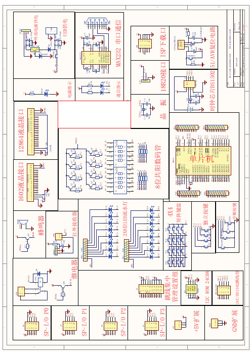
单片机开发板原理图
1122334455667788DDCCAA
TitleNumberRevisionSizeA3Date:2009-12-9Sheet of
File:F:\2008-2 DEMO PCB V2.0.SCHDOCDrawn By
:
EA/VPP31XTAL119XTAL218RST9P3.7(RD)17P3.6(WR)16P3.2(INT0)12P3.3(INT1)13P3.4(T0)14P3.5(T1)15P1.01P1.12P1.23P1.34P1.45P1.5(MOSI)6P1.6(MISO)7P1.7(SCK)8(AD0)P0.039(AD1)P0.138(AD2)P0.237(AD3)P0.336(AD4)P0.435(AD5)P0.534(AD6)P0.633(AD7)P0.732(A8)P2.021(A9)P2.122(A10)P2.223(A11)P2.324(A12)P2.425(A13)P2.526(A14)P2.627(A15)P2.728PSEN29ALE/PROG30(TXD)P3.111(RXD)P3.010GND20VCC40
ZIP40AT8
9
S52
123VinVoutGND
IC17805
12FR1
123DCIN+
+-
-
USB
16V 470uF
C1104pC2104pC416V 470uFC3
PLED1KR1
12POWER
D21N
5819
D11N4007
162738495DB9DB9
C1+1V+2C1-3C2+4C2-5V-6T2OUT7R2IN8R2OUT9T2IN10T1IN11R1OUT12R1IN13T1OUT14GND15
VCC16
IC2M
A
X232
1uFC91uFC8
1uFC71uFC6
10uFC
5
12318B20
CN3
+5
+5
11A121H10F92H83H7B64H1E2D
3DP
4C
5GD
LED1
11A121H10F92H83H7B64H1E2D
3DP
4C
普中科技HC6800V3.0型电路原理图

普中科技HC6800V3.0型电路原理图HC6800型51单片机电路原理图Figure 1 MCU (2)Figure 2 五线四相步进电机 (2)Figure 3四线双极性步进电机 (3)Figure 4 16X16点阵 (3)Figure 5 EEPROM (4)Figure 6 LCD1602 (4)Figure 7 静态数码管 (5)Figure 8 矩阵键盘 (5)Figure 9 独立按键 (6)Figure 10 动态数码管 (6)Figure 11 TFT彩屏 (7)Figure 12 RS485 (7)Figure 13 继电器 (8)Figure 14 蜂鸣器+138译码器 (8)Figure 15 74HC595 (9)Figure 16 74HC165 (10)Figure 17 DS1302+NE555 (11)Figure 18 USB自动下载 (12)Figure 19 使用USB、RS232 + 复位 (12) Figure 20 MAX232 (13)Figure 21 AD/DA/光敏/热敏 (13)Figure 22 交通灯 (14)Figure 23 电源模块 (14)Figure 24 ISP/PS2/温度/红外 (14)Figure 1 MCUFigure 2 五线四相步进电机Figure 3四线双极性步进电机Figure 4 16X16点阵Figure 5 EEPROMFigure 6 LCD1602Figure 7 静态数码管Figure 8 矩阵键盘Figure 9 独立按键Figure 10 动态数码管Figure 11 TFT彩屏Figure 12 RS485Figure 13 继电器Figure 14 蜂鸣器+138译码器Figure 15 74HC595 Figure 16 74HC165Figure 17 DS1302+NE555 Figure 18 USB自动下载Figure 19 使用USB、RS232 + 复位Figure 20 MAX232Figure 21 AD/DA/光敏/热敏Figure 22 交通灯Figure 23 电源模块Figure 24 ISP/PS2/温度/红外。
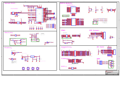
ESP32开发板原理图ESP-WROVER-KIT
R52
100K(1%)
Q2 S8050(NPN) GND IO0
1 3 5 7 9 11 13
2 4 6 8 10 12 14
2 4 6 8 10 12 14
nTRST TMS TDO TDI TCK TDI
MTCK MTDI MTDO MTMS EN
R_IO13 R50 R_IO12 R54 R_IO15 R69 R_IO14 R55 R_nTRSTR58
VDD33
2 3 13
nRXLED nTXLED nPWRSAV nPWREN nSUSPEND
2
R18
R19
R14 C10
XO1 1
12MHz 2 C11 27pF/50V
OSCO
R_IO36 R_IO39 R_IO34 R_IO35 R_IO25 R_IO26 R_IO27 R_IO14 R_IO12
R126 R165 10K(1%) R59 R_IO5 R164 5.1K(1%) Q5 S8050 GND 5.1K(1%) Q4 S8050
15R(1%)
CON7X2_2P54 GND
1 2 3 4 5 6 7 8 9 10 11 12 13 14 15 16 17 18
VDD33
SWITCH BUTTON
SW2 R62 R170 C24 1nF/50V(10%) 10K(1%) R171 1K(1%) 1K(1%)
R172
0R(1%)
IO0 R169 100K(1%) Q9 S8050(NPN) IO2
VDD33 R122 10K(1%)(NC) TDI S_TDI R61 470R(1%) EN R123 C23 1nF/50V(10%) D8 GND GND 10K(1%) C32 0.1uF/25V Q3 S8050(NPN)
米3电路原理图&板位框图

Y5000 32KHz OSC32KO EMCS/WE/CLK/LDM/UDM U5012 LPDDR 64MB EMD*16 EMA*14 JTAG_RSTN/DO/DI/MS/CK
CHG_TORCHEN/AP_FLASHEN USB_HS_ID D_CHG_IRQ_N
U602
VDD_VBUS
VDD_SYS
U1506 气压传感器 BMP180 DS601 FLASH DS602 FLASH FL502 SAW 声表面滤波器 U501 LNA 低噪音放大器 FL501 SAW 声表面滤波器 U500 GPS RX BCM4752 U300 Transceiver SR3500 FL300 SAW GSM/EGSM FL301 SAW DCS/PCS FL302 SAW TD-SCDMA Y501 26MHz WL/BT时钟 U200 AW+PA RF9812 U2006 电压转换器 U2003 LDO 低压差稳压管 U1508 双向电流 和功率监测 U2000 MHL Sil9244 U2001 低噪音 低压差稳压器 Q2000 P沟MOSFET 开关 S2001 USB/MHL 开关 U803 16G eMMC
GPS_CLK_32K_4_U600 GPS_UART2_DTX/DRX/NRTS/NCTS GPS_EN S2001-2
MHL_SEL0 AP_USB_D_P/N S2001-1 J701-2 MHL_SEL0 MHL_D_N MHL_D_N USB_ID U2000 HDMI Sil9244 VDD_VBUS FL2001
HPH_LP PROXIMITY HPH_RN REF HPH_LP HEADSET_MIC/DET DMIC2_SCL/SDA DMIC_SCL/SDA SPK_P/N DMIC_SCL/SDA FL702 EAO_N/P SPKL_N SPKL_P SPK_EN S700 FL701 HPH_RN GEN1_I2C J702 HDST_DET HEADSET_MIC_P_S
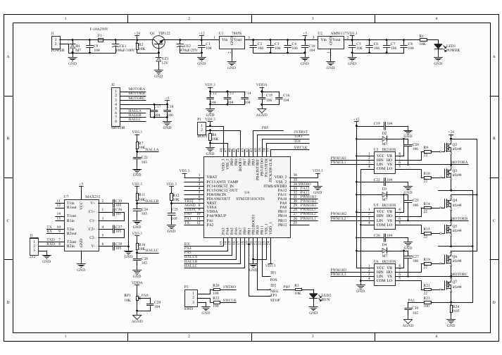
STM32控制的BLDC电机原理图
矿产资源开发利用方案编写内容要求及审查大纲
矿产资源开发利用方案编写内容要求及《矿产资源开发利用方案》审查大纲一、概述
㈠矿区位置、隶属关系和企业性质。
如为改扩建矿山, 应说明矿山现状、
特点及存在的主要问题。
㈡编制依据
(1简述项目前期工作进展情况及与有关方面对项目的意向性协议情况。
(2 列出开发利用方案编制所依据的主要基础性资料的名称。
如经储量管理部门认定的矿区地质勘探报告、选矿试验报告、加工利用试验报告、工程地质初评资料、矿区水文资料和供水资料等。
对改、扩建矿山应有生产实际资料, 如矿山总平面现状图、矿床开拓系统图、采场现状图和主要采选设备清单等。
二、矿产品需求现状和预测
㈠该矿产在国内需求情况和市场供应情况
1、矿产品现状及加工利用趋向。
2、国内近、远期的需求量及主要销向预测。
㈡产品价格分析
1、国内矿产品价格现状。
2、矿产品价格稳定性及变化趋势。
三、矿产资源概况
㈠矿区总体概况
1、矿区总体规划情况。
2、矿区矿产资源概况。
3、该设计与矿区总体开发的关系。
㈡该设计项目的资源概况
1、矿床地质及构造特征。
2、矿床开采技术条件及水文地质条件。
电气化自动技术 6单相桥式全控整流及有源逆变电路实验V3.0版
实验六单相桥式全控整流及有源逆变电路实验一、实验目的(1)加深理解单相桥式全控整流及逆变电路的工作原理。
(2)研究单相桥式变流电路整流的全过程。
(3)研究单相桥式变流电路逆变的全过程,掌握实现有源逆变的条件。
(4)掌握产生逆变颠覆的原因及预防方法。
二、实验所需挂件及附件三、实验线路及原理图3-5为单相桥式整流带电阻电感性负载,其输出负载R用D42三相用DJK02面板上的可调电阻器,将两个900Ω接成并联形式,电抗Ld700mH,直流电压、电流表均在DJK02面板上。
触发电路采用DJK03组件挂箱上的“锯齿波同步移相触发电路Ⅰ”和“Ⅱ”。
图3-6为单相桥式有源逆变原理图,三相电源经三相不控整流,得到一个上负下正的直流电源,供逆变桥路使用,逆变桥路逆变出的交流电压经升压变压器返馈回电网。
“三相不控整流”是DJK10上的一个模块,其“心式变压器”在此做为升压变压器用,从晶闸管逆变出的电压接“心式变压器”的中压端Am、Bm,返回电网的电压从其高压端A、B输出,为了避免输出的逆变电压过高而损坏心式变压器,故将变压器接成Y/Y接法。
图中的电阻R、电抗L d和触发电路与整流所用相同。
有关实现有源逆变的必要条件等内容可参见电力电子技术教材的有关内容。
图3-5 单相桥式整流实验原理图图3-6 单相桥式有源逆变电路实验原理图四、实验内容(1)单相桥式全控整流电路带电阻电感负载。
(2)单相桥式有源逆变电路带电阻电感负载。
(3)有源逆变电路逆变颠覆现象的观察。
五、预习要求(1)阅读电力电子技术教材中有关单相桥式全控整流电路的有关内容。
(2)阅读电力电子技术教材中有关有源逆变电路的内容,掌握实现有源逆变的基本条件。
六、思考题实现有源逆变的条件是什么?在本实验中是如何保证能满足这些条件?七、实验方法(1)触发电路的调试将DJK01电源控制屏的电源选择开关打到“直流调速”侧使输出线电压为200V,用两根导线将200V交流电压接到DJK03的“外接220V”端,按下“启动”按钮,打开DJK03电源开关,用示波器观察锯齿波同步触发电路各观察孔的电压波形。
STM32开发板原理图
R7
45K DC5V
Y1 C2 22pF
R15 DGND DC3.3V R16 R17
10K 30.PA5-SPI1-SCK 10K 31.PA6-SPI1-MISO 10K 32.PA7-SPI1-MOSI A
DC3.3V C A 8550-PNP Q1 E B
R3 10K R4 1K
104
5 9 4 8 3 7 2 6 1
2.4K
ENC28J60CSS (SSOP-28)
RJ45-HR911105A
1 2 3 4 5 6 7 8
DAT2 CD/DAT3 CMD VDD3V CLK VSS DATA0 DATA1 TF_card
1
DC3.3V
DGND
AT24C02(SO-8)
DC5V
60.PD13-LIGHT-PWM 57.PD10-D15
DB9 DB9RA/F
11
1K
10M以太网
DGND C11 U5 10uF 1 2 3 4 5 6 7 8 9 10 11 12 13 14
SPI1
Vcap Vss CLKO INT WOL SO SI SCK CS RST Vssrx TPINTPIN+ Rbias VDD LEDA LEDB Vddosc OSC2 OSC1 Vssosc Vsspll Vddpll Vddrx Vsstx TPOUT+ TPOUTVddtx DC3.3V 28 C13 103 27 26 25 DC3.3V 24 23 22 21 20 19 18 17 16 15 DGND DC3.3V TPOUT+ R21 TPOUT- R22 DC3.3V RJ 1 DGND 2 LEDA 4 LEDB 8 DGND C17 7 C14 20pF 104 C18 104 5 TPIN+ 3 DGND TPIN6 Y2 DGND R24 1K 9 25MHZ 10 C15 20pF R25 1K 12 L1 11 50 DC3.3V A 50 100nH-0805 B C16 103 DGND DGND TPOUT+ TPOUTTD+ TDGND RD+ RDGLEDA GLEDK YLEDA YLEDK A B