GPU架构图
GPU与CPU的区别
GPU与CPU的区别显卡的发展可以说是非常的快,人们对于视觉化上的要求也越来越高,随着用户对于图像处理上面的要求不断超出处理器的计算能力。
另一方面CPU处理能力也不断强大,但在进入3D时代后,人们发现庞大的3D图像处理数据计算使得CPU越来越不堪重荷,并且远远超出其计算能力。
图形计算需求日益增多,作为计算机的显示芯片也飞速发展。
随后人们发现显示芯片的计算能力也无法满足快速增长的图形计算需求时,图形,图像计算等计算的功能被脱离出来单独成为一块芯片设计,这就是现在的图形计算处理器——GPU(Graphics Processing Unit),也就是显卡。
1999年8月,NVIDIA终于正式发表了具有跨世纪意义的产品NV10——GeForce 256。
GeForce256是业界第一款256bit的GPU,也是全球第一个集成T&L(几何加速/转换)、动态光影、三角形设置/剪辑和四像素渲染等3D加速功能的图形引擎。
通过T&L技术,显卡不再是简单像素填充机以及多边形生成器,它还将参与图形的几何计算从而将CPU从繁重的3D管道几何运算中解放出来。
在这代产品中,NVIDIA推出了两个全新的名词——GPU以GeForce。
所以从某种意义上说,GeForce 256开创了一个全新的3D图形时代,NVIDIA终于从追随者走向了领导者。
再到后来GeForce 3开始引出可编程特性,能将图形硬件的流水线作为流处理器来解释,基于GPU的通用计算也开始出现。
到了Nvidia GeForce6800这一代GPU,功能相对以前更加丰富、灵活。
顶点程序可以直接访问纹理,支持动态分支;象素着色器开始支持分支操作,包括循环和子函数调用,TMU 支持64位浮点纹理的过滤和混合,ROP(象素输出单元)支持MRT(多目标渲染)等。
象素和顶点可编程性得到了大大的扩展,访问方式更为灵活,这些对于通用计算而言更是重要突破。
真正意义的变革,是G80的出现,真正的改变随着DX10到来发生质的改变,基于DX10统一渲染架构下,显卡已经抛弃了以前传统的渲染管线,取而代之的是统一流处理器,除了用作图像渲染外,流处理器自身有着强大的运算能力。
gpu 需要掌握的知识
gpu 需要掌握的知识摘要:1.GPU 的概念和历史2.GPU 的主要应用领域3.GPU 的关键技术和架构4.如何学习和掌握GPU 知识5.GPU 的未来发展趋势正文:一、GPU 的概念和历史GPU,全称图形处理器(Graphics Processing Unit),是一种专门用于处理图形和图像任务的微处理器。
GPU 的发展历程可以追溯到上世纪80 年代,从最初的固定功能图形处理器,到90 年代的可编程图形处理器,再到21 世纪初的统一渲染架构,GPU 的性能和功能不断得到提升。
二、GPU 的主要应用领域1.计算机图形学:GPU 主要用于渲染3D 图形和动画,为游戏、电影、广告等提供高质量的视觉效果。
2.机器学习:GPU 可以加速深度学习和其他人工智能任务,提高训练和推理的效率。
3.科学计算:GPU 具有并行处理能力强大的特点,可以高效地处理大规模数据和复杂计算任务,如流体动力学、分子模拟等领域。
三、GPU 的关键技术和架构1.着色器:GPU 的核心部分,负责处理图形和图像的计算任务,包括顶点着色器、片段着色器等。
2.渲染管线:GPU 中用于处理图形和图像的一组指令,包括几何处理、光栅化、纹理贴图等阶段。
3.统一渲染架构:将图形和计算任务统一处理,提高GPU 的通用性和灵活性。
4.并行计算:GPU 具有大量计算单元,可以同时执行多个任务,提高计算效率。
四、如何学习和掌握GPU 知识1.学习基本概念:了解GPU 的定义、历史、应用领域等基本知识。
2.学习GPU 编程:掌握GPU 编程语言(如CUDA、OpenGL 等),编写简单的GPU 程序。
3.学习优化技巧:了解如何优化GPU 程序性能,提高计算效率。
4.实践项目:参与实际项目,积累GPU 编程经验,不断提高自己的技能水平。
五、GPU 的未来发展趋势1.AI 与GPU 的融合:随着人工智能的发展,GPU 将成为AI 计算的重要平台,融合AI 与GPU 技术将是未来的趋势。
图形处理器架构(GPU Architecture)与图形管线(Graphics Pipeline)入门
GPUs-Graphics Processing UnitsMinh Tri Do DinhMinh.Do-Dinh@student.uibk.ac.atVertiefungsseminar Architektur von Prozessoren,SS2008Institute of Computer Science,University of InnsbruckJuly7,2008This paper is meant to provide a closer look at modern Graphics Processing Units.It explorestheir architecture and underlying design principles,using chips from Nvidia’s”Geforce”series asexamples.1IntroductionBefore we dive into the architectural details of some example GPUs,we’ll have a look at some basic concepts of graphics processing and3D graphics,which will make it easier for us to understand the functionality of GPUs1.1What is a GPU?A GPU(G raphics P rocessing U nit)is essentially a dedicated hardware device that is responsible for trans-lating data into a2D image formed by pixels.In this paper,we will focus on the3D graphics,since that is what modern GPUs are mainly designed for.1.2The anatomy of a3D sceneFigure1:A3D scene3D scene:A collection of3D objects and lights.Figure2:Object,triangle and vertices3D objects:Arbitrary objects,whose geometry consists of triangular polygons.Polygons are composed of vertices.Vertex:A Point with spatial coordinates and other information such as color and texture coordinates.Figure3:A cube with a checkerboard textureTexture:An image that is mapped onto the surface of a3D object,which creates the illusion of an object consisting of a certain material.The vertices of an object store the so-called texture coordinates (2-dimensional vectors)that specify how a texture is mapped onto any given surface.Figure4:Texture coordinates of a triangle with a brick textureIn order to translate such a3D scene to a2D image,the data has to go through several stages of a”Graphics Pipeline”1.3The Graphics PipelineFigure5:The3D Graphics PipelineFirst,among some other operations,we have to translate the data that is provided by the application from 3D to2D.1.3.1Geometry StageThis stage is also referred to as the”Transform and Lighting”stage.In order to translate the scene from 3D to2D,all the objects of a scene need to be transformed to various spaces-each with its own coordinate system-before the3D image can be projected onto a2D plane.These transformations are applied on a vertex-to-vertex basis.Mathematical PrinciplesA point in3D space usually has3coordinates,specifying its position.If we keep using3-dimensional vectors for the transformation calculations,we run into the problem that different transformations require different operations(e.g.:translating a vertex requires addition with a vector while rotating a vertex requires multiplication with a3x3matrix).We circumvent this problem simply by extending the3-dimensional vector by another coordinate(the w-coordinate),thus getting what is called homogeneous coordinates.This way, every transformation can be applied by multiplying the vector with a specific4x4matrix,making calculations much easier.Figure6:Transformation matrices for translation,rotation and scalingLighting,the other major part of this pipeline stage is calculated using the normal vectors of the surfaces of an object.In combination with the position of the camera and the position of the light source,one can compute the lighting properties of a given vertex.Figure7:Calculating lightingFor transformation,we start out in the model space where each object(model)has its own coordinate system,which facilitates geometric transformations such as translation,rotation and scaling.After that,we move on to the world space,where all objects within the scene have a unified coordinate system.Figure8:World space coordinatesThe next step is the transformation into view space,which locates a camera in the world space and then transforms the scene,such that the camera is at the origin of the view space,looking straight into the positive z-direction.Now we can define a view volume,the so-called view frustrum,which will be used to decide what actually is visible and needs to be rendered.Figure9:The camera/eye,the view frustrum and its clipping planesAfter that,the vertices are transformed into clip space and assembled into primitives(triangles or lines), which sets up the so-called clipping process.While objects that are outside of the frustrum don’t need to be rendered and can be discarded,objects that are partially inside the frustrum need to be clipped(hence the name),and new vertices with proper texture and color coordinates need to be created.A perspective divide is then performed,which transforms the frustrum into a cube with normalized coordinates(x and y between-1and1,z between0and1)while the objects inside the frustrum are scaled accordingly.Having this normalized cube facilitates clipping operations and sets up the projection into2D space(the cube simply needs to be”flattened”).Figure10:Transforming into clip spaceFinally,we can move into screen space where x and y coordinates are transformed for proper2D display (in a given window).(Note that the z-coordinate of a vertex is retained for later depth operations)Figure11:From view space to screen spaceNote,that the texture coordinates need to be transformed as well and additionally besides clipping,sur-faces that aren’t visible(e.g.the backside of a cube)are removed as well(so-called back face culling).The result is a2D image of the3D scene,and we can move on to the next stage.1.3.2Rasterization StageNext in the pipeline is the Rasterization stage.The GPU needs to traverse the2D image and convert the data into a number of”pixel-candidates”,so-called fragments,which may later become pixels of the final image.A fragment is a data structure that contains attributes such as position,color,depth,texture coordinates,etc.and is generated by checking which part of any given primitive intersects with which pixel of the screen.If a fragment intersects with a primitive,but not any of its vertices,the attributes of that fragment have to be additionally calculated by interpolating the attributes between the vertices.Figure12:Rasterizing a triangle and interpolating its color valuesAfter that,further steps can be made to obtain thefinal pixels.Colors are calculated by combining textures with other attributes such as color and lighting or by combining a fragment with either another translucent fragment(so-called alpha blending)or optional fog(another graphical effect).Visibility checks are performed such as:•Scissor test(checking visibility against a rectangular mask)•Stencil test(similar to scissor test,only against arbitrary pixel masks in a buffer)•Depth test(comparing the z-coordinate of fragments,discarding those which are further away)•Alpha test(checking visibility against translucent fragments)Additional procedures like anti-aliasing can be applied before we achieve thefinal result:a number of pixels that can be written into memory for later display.This concludes our short tour through the graphics pipeline,which hopefully gives us a better idea of what kind of functionality will be required of a GPU.2Evolution of the GPUSome historical key points in the development of the GPU:•Efforts for real time graphics have been made as early as1944(MIT’s project”Whirlwind”)•In the1980s,hardware similar to modern GPUs began to show up in the research community(“Pixel-Planes”,a a parallel system for rasterizing and texture-mapping3D geometry•Graphic chips in the early1980s were very limited in their functionality•In the late1980s and early1990s,high-speed,general-purpose microprocessors became popular for implementing high-end GPUs(e.g.Texas Instruments’TMS340)•1985Thefirst mass-market graphics accelerator was included in the Commodore Amiga•1991S3introduced thefirst single chip2D-accelerator,the S386C911•1995Nvidia releases one of thefirst3D accelerators,the NV1•1999Nvidia’s Geforce256is thefirst GPU to implement Transform and Lighting in Hardware •2001Nvidia implements thefirst programmable shader units with the Geforce3•2005ATI develops thefirst GPU with unified shader architecture with the ATI Xenos for the XBox 360•2006Nvidia launches thefirst unified shader GPU for the PC with the Geforce88003From Theory to Practice-the Geforce68003.1OverviewModern GPUs closely follow the layout of the graphics pipeline described in thefirst ing Nvidia’s Geforce6800as an example we will have a closer look at the architecture of modern day GPUs.Since being founded in1993,the company NVIDIA has become one of the biggest manufacturers of GPUs (besides ATI),having released important chips such as the Geforce256,and the Geforce3.Launched in2004,the Geforce6800belongs to the Geforce6series,Nvidia’s sixth generation of graphics chipsets and the fourth generation that featured programmability(more on that later).The following image shows a schematic view of the Geforce6800and its functional units.Figure13:Schematic view of the Geforce6800You can already see how each of the functional units correspond to the stages of the graphics pipeline. We start with six parallel vertex processors that receive data from the host(the CPU)and perform oper-ations such as transformation and lighting.Next,the output goes into the triangle setup stage which takes care of primitive assembly,culling and clipping,and then into the rasterizer which produces the fragments.The Geforce6800has an additional Z-cull unit which allows to perform an early fragment visibility check based on depth,further improving the efficiency.We then move on to the sixteen fragment processors which operate in4parallel units and computes the output colors of each fragment.The fragment crossbar is a linking element that is basically responsible for directing output pixels to any available pixel engine(also called ROP,short for R aster O perator),thus avoiding pipeline stalls.The16pixel engines are thefinal stage of processing,and perform operations such as alpha blending, depth tests,etc.,before delivering thefinal pixel to the frame buffer.3.2In DetailFigure14:A more detailed view of the Geforce6800While most parts of the GPU arefixed function units,the vertex and fragment processors of the Geforce 6800offer programmability which wasfirst introduced to the geforce chipset line with the geforce3(2001). We’ll have a more detailed look at the units in the following sections.3.2.1Vertex ProcessorFigure15:A vertex processorThe vertex processors are the programmable units responsible for all the vertex transformations and at-tribute calculations.They operate with4-dimensional data vectors corresponding with the aforementioned homogeneous coordinates of a vertex,using32bits per coordinate(hence the128bits of a register).Instruc-tions are123bits long and are stored in the Instruction RAM.The data path of a vertex processor consists of:•A multiply-add unit for4-dimensional vectors•A scalar special function unit•A texture unitInstruction set:Some notable instructions for the vertex processor include:dp4dst,src0,src1Computes the four-component dot product of the source registersexp dst,src Provides exponential2xdst dest,src0,src1Calculates a distance vectornrm dst,src Normalize a3D vectorrsq dst,src Computes the reciprocal square root(positive only)of the sourcescalarRegisters in the vertex processor instructions can be modified(with few exceptions):•Negate the register value•Take the absolute value of the register•Swizzling(copy any source register component to any temporary register component)•Mask destination register componentsOther technical details:•Vertex processors are MIMD units(Multiple Instruction Multiple Data)•They use VLIW(Very Long Instruction Words)•They operate with32-bitfloating point precision•Each vertex processor runs up to3threads to hide latency•Each vertex processor can perform a four-wide MAD(Multiply-Add)and a special function in one cycle3.2.2Fragment ProcessorFigure16:A fragment processorThe Geforce6800has16fragment processors.They are grouped to4bigger units which operate simulta-neously on4fragments each(a so-called quad).They can take position,color,depth,fog as well as other arbitrary4-dimensional attributes as input.The data path consists of:•An Interpolation block for attributes•2vector math(shader)units,each with slightly different functionality•A fragment texture unitSuperscalarity:A fragment processor works with4-vectors(vector-oriented instruction set),where sometimes components of the vector need be treated seperately(e.g.color,alpha).Thus,the fragment processor supports co-issueing of the data,which means splitting the vector into2parts and executing different operations on them in the same clock.It supports3-1and2-2splitting(2-2co-issue wasn’t possible earlier).Additionally,it also features dual issue,which means executing different operations on the2vector math units in the same clock.Texture Unit:The texture unit is afloating-point texture processor which fetches andfilters the texture data.It is con-nected to a level1texture cache(which stores parts of the textures that are used).Shader units1and2:Each shader unit is limited in its abilities,offering complete functionality when used together.Figure17:Block diagram of Shader Unit1and2Shader Unit1:Green:A crossbar which distributes the input coming eiter from the rasterizer or from the loopback Red:InterpolatorsYellow:A special function unit(for functions such as Reciprocal,Reciprocal Square Root,etc.)Cyan:MUL channelsOrange:A unit for texture operations(not the fragment texture unit)The shader unit can perform2operations per clock:A MUL on a3-dimensional vector and a special function,a special function and a texture operation,or2 MULs.The output of the special function unit can go into the MUL channels.The texture gets input from the MUL unit and does LOD(Level Of Detail)calculations,before passing the data to the actual fragment texture unit.The fragment texture unit then performs the actual sampling and writes the data into registers for the second shader unit.The shader unit can simply pass data as well.Shader Unit2:Red:A crossbarCyan:4MUL channelsGray:4ADD channelsYellow:1special function unitThe crossbar splits the input onto5channels(4components,1channel stays free).The ADD units are additionally connected,allowing advanced operations such as a dotproduct in one clock. Again,the shader unit can handle2independent operations per cycle or it can simply pass data.If no special function is used,the MAD unit can perform up to2operations from this list:MUL,ADD,MAD,DP,or any other instruction based on these operations.Instruction set:Some notable instructions for the vertex processor include:cmp dst,src0,src1,src2Choose src1if src0>=0.Otherwise,choose src2.The comparisonis done per channeldsx dst,src Compute the rate of change in the render target’s x-directiondsy dst,src Compute the rate of change in the render target’s y-direction sincos dst.{x|y|xy},src0.{x|y|z|w}Computes sine and cosine,in radianstexld dst,src0,src1Sample a texture at a particular sampler,using provided texturecoordinatesRegisters in the fragment processor instructions can be modified(with few exceptions):•Negate the register value•Take the absolute value of the register•Mask destination register componentsOther technical details:•The fragment processors can perform operations within16or32floating point precision(e.g.the fog unit uses only16bit precision for its calculations since that is sufficient)•The quads operate as SIMD units•They use VLIW•They run up to100s of threads to hide texture fetch latency(˜256per quad)•A fragment processor can perform up to8operations per cycle/4math operations if there’s a texture fetch in shader1Figure18:Possible operations per cycle•The fragment processors have a2level texture cache•The fog unit can perform fog blending on thefinal pass without performance penalty.It is implemented withfixed point precision since that’s sufficient for fog and saves performance.The equation:out=FogColor*fogFraction+SrcColor*(1-fogFraction)•There’s support for multiple render targets,the pixel processor can output to up to four seperate buffers(4x4values,color+depth)3.2.3Pixel EngineFigure19:A pixel engineLast in the pipeline are the16pixel engines(raster operators).Each pixel engine connects to a specific memory partition of the GPU.After the lossless color and depth compression,the depth and color units perform depth,color and stencil operations before writing thefinal pixel.When activated the pixel engines also perform multisample antialiasing.3.2.4MemoryFrom“GPU Gems2,Chapter30:The GeForce6Series GPU Architecture”:“The memory system is partitioned into up to four independent memory partitions,eachwith its own dynamic random-access memories(DRAMs).GPUs use standard DRAM modulesrather than custom RAM technologies to take advantage of market economies and thereby reducecost.Having smaller,independent memory partitions allows the memory subsystem to operateefficiently regardless of whether large or small blocks of data are transferred.All rendered surfacesare stored in the DRAMs,while textures and input data can be stored in the DRAMs or insystem memory.The four independent memory partitions give the GPU a wide(256bits),flexible memory subsystem,allowing for streaming of relatively small(32-byte)memory accessesat near the35GB/sec physical limit.”3.3Performance•425MHz internal graphics clock•550MHz memory clock•256-MB memory size•35.2GByte/second memory bandwidth•600million vertices/second•6.4billion texels/second•12.8billion pixels/second,rendering z/stencil-only(useful for shadow volumes and shadow buffers)•6four-wide fp32vector MADs per clock cycle in the vertex shader,plus one scalar multifunction operation(a complex math operation,such as a sine or reciprocal square root)•16four-wide fp32vector MADs per clock cycle in the fragment processor,plus16four-wide fp32 multiplies per clock cycle•64pixels per clock cycle early z-cull(reject rate)•120+Gflops peak(equal to six5-GHz Pentium4processors)•Up to120W energy consumption(the card has two additional power connectors,the power sources are recommended to be no less than480W)4Computational PrinciplesStream Processing:Typical CPUs(the von Neumann architecture)suffer from memory bottlenecks when processing.GPUs are very sensitive to such bottlenecks,and therefore need a different architecture,they are essentially special purpose stream processors.A stream processor is a processor that works with so-called streams and kernels.A stream is a set of data and a kernel is a small program.In stream processors,every kernel takes one or more streams as input and outputs one or more streams,while it executes its operations on every single element of the input streams. In stream processors you can achieve several levels of parallelism:•Instruction level parallelism:kernels perform hundreds of instructions on every stream element,you achieve parallelism by performing independent instructions in parallel•Data level parallelism:kernels perform the same instructions on each stream element,you achieve parallelism by performing one instruction on many stream elements at a time•Task level parallelism:Have multiple stream processors divide the work from one kernelStream processors do not use caching the same way traditional processors do since the input datasets are usually much larger than most caches and the data is barely reused-with GPUs for example the data is usually rendered and then discarded.We know GPUs have to work with large amounts of data,the computations are simpler but they need to be fast and parallel,so it becomes clear that the stream processor architecture is very well suited for GPUs. Continuing these ideas,GPUs employ following strategies to increase output:Pipelining:Pipelining describes the idea of breaking down a job into multiple components that each perform a single task.GPUs are pipelined,which means that instead of performing complete processing of a pixel before moving on to the next,youfill the pipeline like an assembly line where each component performs a task on the data before passing it to the next stage.So while processing a pixel may take multiple clock cycles,you still achieve an output of one pixel per clock since youfill up the whole pipe.Parallelism:Due to the nature of the data-parallelism can be applied on a per-vertex or per-pixel basis -and the type of processing(highly repetitive)GPUs are very suitable for parallelism,you could have an unlimited amount of pipelines next to each other,as long as the CPU is able to keep them busy.Other GPU characteristics:•GPUs can afford large amounts offloating point computational power since they have lower control overhead•They use dedicated functional units for specialized tasks to increase speeds•GPU memory struggles with bandwidth limitations,and therefore aims for maximum bandwidth usage, employing strategies like data compression,multiple threads to cope with latency,scheduling of DRAM cycles to minimize idle data-bus time,etc.•Caches are designed to support effective streaming with local reuse of data,rather than implementinga cache that achieves99%hit rates(which isn’t feasible),GPU cache designs assume a90%hit ratewith many misses inflight•GPUs have many different performance regimes all with different characteristics and need to be de-signed accordingly4.1The Geforce6800as a general processorYou can see the Geforce6800as a general processor with a lot offloating-point horsepower and high memory bandwidth that can be used for other applications as well.Figure20:A general view of the Geforce6800architectureLooking at the GPU that way,we get:•2serially running programmable blocks with fp32capability.•The Rasterizer can be seen as a unit that expands the data into interpolated values(from one data-”point”to multiple”fragments”).•With MRT(Multiple Render Targets),the fragment processor can output up to16scalarfloating-point values at a time.•Several possibilities to control the dataflow by using the visibility checks of the pixel engines or the Z-cull unit5The next step:the Geforce8800After the Geforce7series which was a continuation of the Geforce6800architecture,Nvidia introduced the Geforce8800in2006.Driven by the desire to increase performance,improve image quality and facilitate programming,the Geforce8800presented a significant evolution of past designs:a unified shader architec-ture(Note,that ATI already used this architecture in2005with the XBOX360GPU).Figure21:From dedicated to unified architectureFigure22:A schematic view of the Geforce8800The unified shader architecture of the Geforce8800essentially boils down to the fact that all the different shader stages become one single stage that can handle all the different shaders.As you can see in Figure22,instead of different dedicated units we now have a single streaming processor array.We have familiar units such as the raster operators(blue,at the bottom)and the triangle setup, rasterization and z-cull unit.Besides these units we now have several managing units that prepare and manage the data as itflows in the loop(vertex,geometry and pixel thread issue,input assembler and thread processor).Figure23:The streaming processor arrayThe streaming processor array consists of8texture processor clusters.Each texture processor cluster in turn consists of2streaming multiprocessors and1texture pipe.A streaming multiprocessor has8streaming processors and2special function units.The streaming pro-cessors work with32-bit scalar data,based on the idea that shader programs are becoming more and more scalar,making a vector architecture more inefficient.They are driven by a high-speed clock that is seperate from the core clock and can perform a dual-issued MUL and MAD at each cycle.Each multiprocessor can have768hardware scheduled threads,grouped together to24SIMD”warps”(A warp is a group of threads). The texture pipe consists of4texture addressing and8texturefiltering units.It performs texture prefetching andfiltering without consuming ALU resources,further increasing efficency.It is apparent that we gain a number of advanteges with such a new architecture.For example,the old problem of constantly changing workload and one shader stage becoming a processing bottleneck is solved since the units can adapt dynamically,now that they are unified.Figure24:Workload balancing with both architecturesWith a single instruction set and the support of fp32throughout the whole pipeline,as well as the support of new data types(integer calculations),programming the GPU now becomes easier as well.6General Purpose Programming on the GPU-an exampleWe use the bitonic merge sort algorithm as an example for efficiently implementing algorithms on a GPU. Bitonic merge sort:Bitonic merge sort works by repeatedly building bitonic lists out of a set of elements and sorting them.A bitonic list is a concatenation of two monotonic lists,one ascending and one descending.E.g.:List A=(3,4,7,8)List B=(6,5,2,1)List AB=(3,4,7,8,6,5,2,1)is a bitonic listList BA=(6,5,2,1,3,4,7,8)is also a bitonic listBitonic lists have a special property that is used in bitonic mergesort:Suppose you have a bitonic list of length2n.You can rearrange the list so that you get two halves with n elements where each element(i)of thefirst half is less than or equal to each corresponding element(i+n)in the second half(or greater than or equal,if the list descendsfirst and then ascends)and the new list is again a bitonic list.This happens by com-paring the corresponding elements and switching them if necessary.This procedure is called a bitonic merge. Bitonic merge sort works by recursively creating and merging bitonic lists that increase in their size until we reach the maximum size and the complete list is sorted.Figure25illustrates the process:Figure25:The different stages of the algorithmThe sorting process has a certain number of stages where comparison passes are performed.Each new stage increases the number of passes by one.This results in bitonic mergesort having a complexity of O(n log2(n)+log(n))which is worse than quicksort,but the algorithm has no worst-case scenario(where quicksort reaches O(n2).The algorithm is very well suited for a GPU.Many of the operations can be performed in parallel and the length stays constant,given a certain number of elements.Now when implementing this algorithm on the GPU,we want to make use of as many resources as possible(both in parallel as well as vertically alongthe pipeline),especially considering that the GPU has shortcomings as well,such as the lack of support for binary or integer operations.For example,simply letting the fragment processor stage handle all the calculations might work,but leaving all the other units unused is a waste of precious resources.A possible solution looks like this:In this algorithm,we have groups of elements(fragments)that have the same sorting conditions,while groups next to each other operate in opposite.Now if we draw a vertex quad over two adjacent groups and set appropriateflags at each corner,we can easily determine group membership by using the rasterizer.For example,if we set the left corners to-1and the right corners to+1,we can check where a fragment belongs to by simply looking at its sign(the interpolation process takes care of that).Figure26:Using vertexflags and the interpolator to determine compare operationsNext,we need to determine which compare operation to use and we need to locate the partner item to compare.Both can again be accomplished by using theflag value.Setting the compare operation to less-than and multiplying with theflag value implicitlyflips the operation to greater-equal halfway across the quad. Locating the partner item happens by multiplying the sign of theflag with an absolute value that specifies the distance between the items.In order to sort elements of an array,we store them in a2D texture.Each row is a set of elements and becomes its own bitonic sequence that needs to be sorted.If we extend the quads over the rows of the2D texture and use the interpolation,we can modulate the comparison so the rows get sorted either up or down according to their row number.This way,pairs of rows become bitonic sequences again which can besorted in the same way we sorted the columns of the single rows,simply by transposing the quads.As afinal optimization we reduce texture fetching by packing two neighbouring key pairs into one frag-ment,since the shader operates on4-vectors.Performance comparison:std:sort:16-Bit Data, Pentium43.0GHz Bitonic Merge Sort:16-Bit Float Data, NVIDIA Geforce6800UltraN FullSorts/Sec SortedKeys/SecN Passes FullSorts/SecSortedKey/Sec256282.5 5.4M256212090.07 6.1M 512220.6 5.4M512215318.3 4.8M 10242 4.7 5.0M10242190 3.6 3.8M。
华为FusionCube系统构架介绍
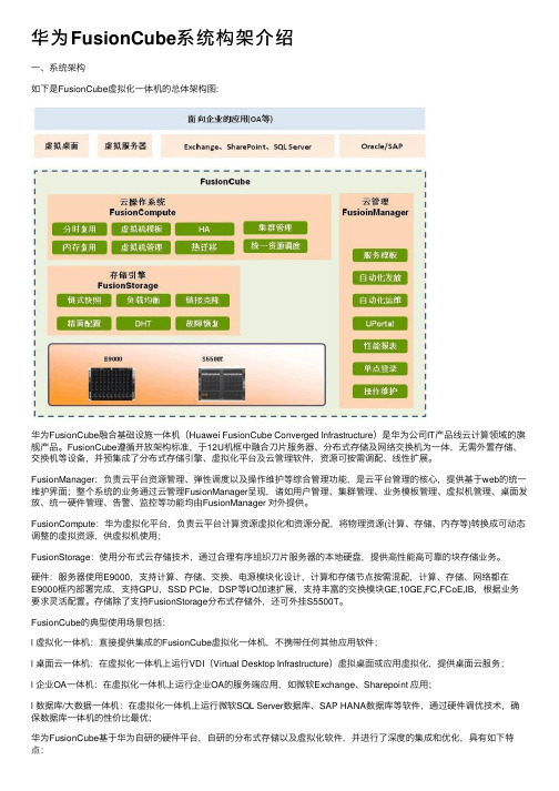
华为FusionCube系统构架介绍⼀、系统架构如下是FusionCube虚拟化⼀体机的总体架构图:华为FusionCube融合基础设施⼀体机(Huawei FusionCube Converged Infrastructure)是华为公司IT产品线云计算领域的旗舰产品。
FusionCube遵循开放架构标准,于12U机框中融合⼑⽚服务器、分布式存储及⽹络交换机为⼀体,⽆需外置存储、交换机等设备,并预集成了分布式存储引擎、虚拟化平台及云管理软件,资源可按需调配、线性扩展。
FusionManager:负责云平台资源管理、弹性调度以及操作维护等综合管理功能,是云平台管理的核⼼,提供基于web的统⼀维护界⾯;整个系统的业务通过云管理FusionManager呈现,诸如⽤户管理、集群管理、业务模板管理、虚拟机管理、桌⾯发放、统⼀硬件管理、告警、监控等功能均由FusionManager 对外提供。
FusionCompute:华为虚拟化平台,负责云平台计算资源虚拟化和资源分配,将物理资源(计算、存储、内存等)转换成可动态调整的虚拟资源,供虚拟机使⽤;FusionStorage:使⽤分布式云存储技术,通过合理有序组织⼑⽚服务器的本地硬盘,提供⾼性能⾼可靠的块存储业务。
硬件:服务器使⽤E9000,⽀持计算、存储、交换、电源模块化设计,计算和存储节点按需混配,计算、存储、⽹络都在E9000框内部署完成,⽀持GPU,SSD PCIe,DSP等I/O加速扩展,⽀持丰富的交换模块GE,10GE,FC,FCoE,IB,根据业务要求灵活配置。
存储除了⽀持FusionStorage分布式存储外,还可外挂S5500T。
FusionCube的典型使⽤场景包括:l 虚拟化⼀体机:直接提供集成的FusionCube虚拟化⼀体机,不携带任何其他应⽤软件;l 桌⾯云⼀体机:在虚拟化⼀体机上运⾏VDI(Virtual Desktop Infrastructure)虚拟桌⾯或应⽤虚拟化,提供桌⾯云服务;l 企业OA⼀体机:在虚拟化⼀体机上运⾏企业OA的服务端应⽤,如微软Exchange、Sharepoint 应⽤;l 数据库/⼤数据⼀体机:在虚拟化⼀体机上运⾏微软SQL Server数据库、SAP HANA数据库等软件,通过硬件调优技术,确保数据库⼀体机的性价⽐最优;华为FusionCube基于华为⾃研的硬件平台,⾃研的分布式存储以及虚拟化软件,并进⾏了深度的集成和优化,具有如下特点:l 简单易⽤FusionCube将服务器、存储和⽹络打包放置在统⼀的机框或机架中,从销售到维护都更简单;l 业务快速部署可以快速部署系统,灵活为企业分配IT资源。
如何使用GPU-Z查看显卡的各项性能
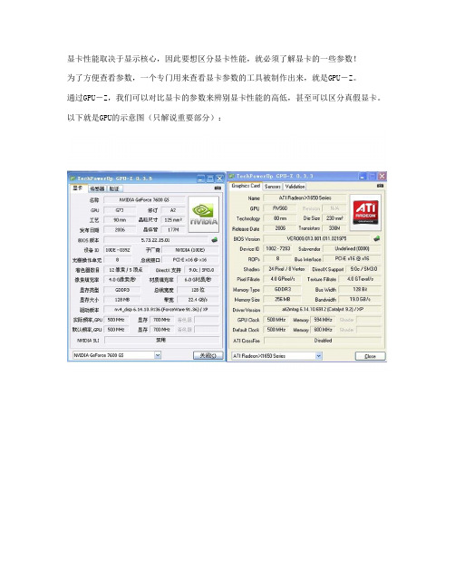
显卡性能取决于显示核心,因此要想区分显卡性能,就必须了解显卡的一些参数!为了方便查看参数,一个专门用来查看显卡参数的工具被制作出来,就是GPU-Z。
通过GPU-Z,我们可以对比显卡的参数来辨别显卡性能的高低,甚至可以区分真假显卡。
以下就是GPU的示意图(只解说重要部分):【名称】:可以直接显示是哪个芯片公司生产的型号注:Nvidia可以直接显示出具体型号,例如图直接注明7600GSATI 只会显示显卡的同系列名称,例如X1650GT只显示1650 Series【GPU】:显示核芯,核芯代号,所指的是研发公司内部编号,也可以用于区分性能高低。
【工艺】:核心的制作工艺,单位纳米,越小工艺就越先进,功耗就越低。
【光栅】:数量越高,显卡性能越强。
光栅属于输出单元,负责后期渲染,将像素点光栅化,主要影响抗锯齿、动态模糊之类特效,但对光线却没什么大的影响。
【总线接口】:提供数据流量带宽,目前主流的接口是PCI-E 16×,可以提供8G/s的数据流量(双通道,上、下行各4G/s)。
注:16×@16×,代表最高支持流量,以及目前工作的流量,如果主板或者电源影响,工作接口有可能会下降!【着色器】:旧架构为“渲染管线+着色顶点”,新架构之后统一为“统一渲染单元”,即“流处理器”,数量越高性能越好。
旧架构区分性能通过“渲染管线”多少、“着色顶点”多少就可以了解显卡性能。
新架构由于只有一个基数,因此更容易了解,数值越高性能越强。
注:N卡一个流处理器就能发挥作用,因此流处理器数量看上去很少。
A卡对“统一渲染单元”定位不一样,要5个流处理器单元一组才能工作,因此看上去数量很高。
【Directx 支持】:简称DX,是微软编写的程序,作用于多媒体指令,在显卡方面,就是针对画面特效,目前最高级别是DX11(Windows 7)。
【像数填充率】:光栅工作的数据处理流量,公式GPU频率×光栅=像数填充率。
高通Adreno图形处理器解析
手机GPU:高通Adreno图形处理器解析高通(Qualcomm)不只是一家在移动SoC芯片和3G通信技术上造诣颇深的公司,而且是一家拥有移动GPU自主设计能力和生产能力的公司。
移动GPU是SoC 芯片的一部分,与ARM架构的通用处理器(CPU)一起构成SoC芯片体现应用性能的两个重要部分。
美国高通公司目前除高通公司对应用在手机和平板电脑领域的GPU进行设计和生产以外,另外还有两家公司也从事这方面的开发,它们是Imagination公司和ARM公司,他们对应的产品分别是PowerVR SGX系列和Mali系列(移动GPU:ARM Mali图形处理单元全解析)。
高通GPU历史:高通公司的GPU业务发展时间较短,但是如果追溯它的根源,却可以说由来已久。
2004年,高通与加拿大图形芯片设计公司ATI Technologies达成合作计划,决定把该公司的3D图形技术集成到高通Qualcomm的下一代芯片中去。
之后,高通引进ATI的Imageon图形平台,并将Imageon技术集成到Qualcomm的7000系列移动站点调制解调器手机芯片中。
高通收购AMD相关图形芯片部门在以后的数年时间里,高通与ATI展开了手机芯片的密切合作。
2006年,ATI 被AMD收购。
直至2009年初,高通传出收购AMD包括绘图芯片技术在内的掌上设备资产,将这部分技术包括产权收于囊中。
至此,高通不必再为绘图核心技术的授权买单。
高通是否收购了AMD的Imageon部门?我们知道,高通收购了AMD的绘图芯片技术相关资源。
但是AMD表示,高通收购的部分是“向量绘图(vectorgraphics)与3D绘图技术和知识产权(IP)”,这部分特定的资产技术是AMD之前未曾揭露过的,而不包括Imageon处理器产品、Imageon 品牌。
QUALCOMM高通除了出售给高通的图形技术产权以外,AMD自家依然保留Imageon处理器品牌,AMD的掌上型绘图技术集中在“unified shader architecture”技术,这项技术已授权给微软Xbox及其他厂商使用,与售给高通的技术并无太大关系。
CUDA---GPU架构知识技巧
GPU架构SM(Streaming Multiprocessors)是GPU架构中非常重要的部分,GPU硬件的并行性就是由SM决定的。
以Fermi架构为例,其包含以下主要组成部分:∙CUDA cores∙Shared Memory/L1Cache∙Register File∙Load/Store Units∙Special Function Units∙Warp SchedulerGPU中每个SM都设计成支持数以百计的线程并行执行,并且每个GPU 都包含了很多的SM,所以GPU支持成百上千的线程并行执行,当一个kernel启动后,thread会被分配到这些SM中执行。
大量的thread 可能会被分配到不同的SM,但是同一个block中的thread必然在同一个SM中并行执行。
CUDA采用Single Instruction Multiple Thread(SIMT)的架构来管理和执行thread,这些thread以32个为单位组成一个单元,称作warps。
warp中所有线程并行的执行相同的指令。
每个thread拥有它自己的instruction address counter和状态寄存器,并且用该线程自己的数据执行指令。
SIMT和SIMD(Single Instruction, Multiple Data)类似,SIMT 应该算是SIMD的升级版,更灵活,但效率略低,SIMT是NVIDIA提出的GPU新概念。
二者都通过将同样的指令广播给多个执行官单元来实现并行。
一个主要的不同就是,SIMD要求所有的vector element 在一个统一的同步组里同步的执行,而SIMT允许线程们在一个warp 中独立的执行。
SIMT有三个SIMD没有的主要特征:∙每个thread拥有自己的instruction address counter∙每个thread拥有自己的状态寄存器∙每个thread可以有自己独立的执行路径一个block只会由一个SM调度,block一旦被分配好SM,该block 就会一直驻留在该SM中,直到执行结束。
了解电脑硬件CPU和GPU的区别
了解电脑硬件CPU和GPU的区别在如今数字化浪潮的时代,电脑已经成为人们生活和工作中不可或缺的工具。
而电脑的硬件组成部分被广泛认为是其中最重要的部分。
其中两个核心组成部分分别是CPU(中央处理器)和GPU(图形处理器)。
尽管它们都属于处理器的范畴,但是CPU和GPU在设计和功能上有很大的区别。
本文将重点解释CPU和GPU之间的差异,帮助读者更好地了解这两个关键部件。
一、CPU与GPU的定义1. CPU(中央处理器)CPU,全称为中央处理器(Central Processing Unit),是一种负责执行各种计算任务的芯片,是电脑的核心处理器。
它是电脑的“大脑”,负责解析和执行指令,管理和协调电脑的各个组件。
2. GPU(图形处理器)GPU,全称为图形处理器(Graphics Processing Unit),是电脑中的另一种处理器。
与CPU相比,GPU的主要任务是处理图形和图像相关的任务,特别是3D图形处理。
二、CPU与GPU的架构差异1. 架构设计CPU的设计主要针对通用计算任务,其架构更加多功能和灵活。
它具备更高的时钟频率、更大的缓存容量和更强的单线程性能,适合处理各种任务,如软件运行、文件管理和网络通讯等。
GPU的架构则更加专注于处理并行计算任务,特别是图形处理。
它拥有大量的核心,且这些核心可以并行处理大量数据,以实现高效的图像渲染和计算。
2. 并行计算能力CPU在设计上更适合串行计算任务,它的每个核心可以处理多个任务,但是对于大规模并行计算任务,CPU相对较慢。
GPU则是为了并行计算而设计的,它具有大量的核心和强大的内存带宽,可以同时处理大量的并行任务。
这使得GPU在图像、视频处理和科学计算等方面具有明显的优势。
三、CPU与GPU的应用领域差异1. CPU的应用领域由于其灵活性和通用性,CPU广泛应用于各个领域。
例如,它们用于操作系统的运行、网页浏览、文字处理、办公软件以及一些需要高度交互和实时性的任务,如游戏和视频剪辑等。
移动端Tile-Base架构GPU及优化方法
Tile-Base GPU以及优化思路Tile-Based GPU 架构,也称为Tile-Based Rendering(TBR)或Tile-Based Deferred Rendering(TBDR),是一种现代移动端GPU 的设计架构,它将屏幕分成一个个的区块(tile),每个区块的坐标通过中间缓冲器以列表形式保存在系统内存中,GPU 一次只绘制一个tile。
相比传统的Immediate Mode Rendering(IMR)架构,TBR/TBDR 架构在移动端设备上具有一些优势,如减少带宽开销、降低功耗等。
TBR/TBDR 架构的工作原理可以分为两个主要阶段:Binning Pass 和Rendering Pass。
在Binning Pass 阶段,GPU 会处理所有的顶点,并将每个图元分配到对应的tile 中。
这个过程会生成一个tile list 的中间数据(FrameData),其中保存了每个图元所属的tile 坐标。
对于不同的GPU 架构,tile 的大小可能会有所不同,例如PowerVR 的tile 大小为32x32,而Mali 的tile 大小为16x16。
在rendering Pass 阶段,GPU 会针对每个tile 执行像素处理过程,包括光栅化、片元着色器等。
每个tile 处理完毕后,将结果一起写入到系统内存中。
由于每个tile 的大小较小,其对应的framebuffer 可以存放在on-chip memory 上,从而减少了对主存的访问,降低了带宽开销。
此外,depth buffer 和stencil buffer 只在tile 处理内部有用,不需要写回系统内存,进一步节省了带宽。
与传统的IMR 架构相比,TBR/TBDR 架构在处理遮挡关系时具有一定的优势。
在IMR 架构中,即使一个图元被其他图元遮挡,也需要对其进行像素处理。
而在TBDR 架构中,通过隐面剔除(Hidden Surface Removal)技术,可以在Binning Pass 阶段提前剔除那些被遮挡的图元,从而避免了不必要的像素处理,提高了性能。
解读ARM架构主流GPU
解读ARM架构主流GPUGPU一词是由英伟达在1999年提出来的。
GPU相当于专用于图像处理的CPU,正因为它专,所以它强,在处理图像时它的工作效率远高于CPU,因此在PC时代,一个带有不错GPU的独立显卡无疑是游戏玩家的必然选择。
而在智能手机飞速发展的这两年,特别是cortex—A8规格的CPU的使用,手机CPU的主频也达到了1GB,硬件性能也成为了智能手机好坏的重要标志。
在加上软件商城那些游戏软件的催化,一个不错的GPU对主流的智能手机无疑是必须的。
在android平台中,由于没有一个同一的硬件标准,导致了各个厂家,各个型号的手机的硬件就不一样。
目前应用在手机和平板电脑端的GPU主要由四家公司执行设计——英伟达、Imagination公司、高通公司和ARM公司。
其中,ARM和Imagination公司并不进行GPU 的实际生产,而是主要出售芯片设计技术(IP)的授权。
Imagination公司以著名的PowerVR SGX系列为主,CPU包括TI的OMAP系列、三星的S5PC100/C110/S5PV210、苹果的A4/A5等等都是用这个系列的GPU.ARM公司则包括是Mali系列,型号为Mali-55、Mali-200、Mali-300、Mali-400、Mali-T604等,其授权的厂商较多,但是在智能手机上的应用很少见,一般在平板上,如最近较火的智器T10、蓝魔W10就是搭载的AMLogic AML8726-M型号的cpu就是整合了Mali-400型号GPU.高通的产品主要是Adreno系列被广泛的采用在高通的Snapdragon平台上,目前主流是Adreno 130、dreno 200以及高端的Adreno 205。
英伟达的在智能上的GPU主要就是搭载图睿2上得GeForce ULV,它无疑也是第一款开卖的双核智能手机上的GPU,代表机型为摩托的ATRTX 4G和LG的擎天柱了。
除此之外还有不常见的如Vivante的GCXXX,和博通的BCM27xx等等,可能要到年中之后才能大规模进入智能手机市场。
- 1、下载文档前请自行甄别文档内容的完整性,平台不提供额外的编辑、内容补充、找答案等附加服务。
- 2、"仅部分预览"的文档,不可在线预览部分如存在完整性等问题,可反馈申请退款(可完整预览的文档不适用该条件!)。
- 3、如文档侵犯您的权益,请联系客服反馈,我们会尽快为您处理(人工客服工作时间:9:00-18:30)。
显卡帝教你读懂GPU架构图轻松做达人GPU架构“征途之旅”即日起航显卡GPU架构之争永远是DIY玩家最津津乐道的话题之一,而对于众多普通玩家来说经常也就看看热闹而已。
大多数玩家在购买显卡的时候其实想的是这款显卡是否可以满足我实际生活娱乐中的应用要求,而不大会很深入的关注GPU的架构设计。
不过,如果你想成为一个资深DIY玩家,想与众多DIY高手“高谈阔论”GPU架构设计方面的话题的时候,那么你首先且必须弄明白显卡GPU 架构设计的基本思想和基本原理,而读懂GPU架构图正是这万里长征的第一步。
显卡帝手把手教你读懂GPU架构图通过本次GPU架构图的“征途之旅”,网友朋友将会和显卡帝共同来探讨和解密如下问题:一、顶点、像素、着色器是什么;二、SIMD与MIMD的架构区别;三、A/N在统一渲染架构革新中的三次交锋情况如何;四、为什么提出并行架构设计;五、A/N两家在GPU架构设计的特点及其异同点是什么。
以上目录也正是本文的大致行文思路,显卡帝希望能够通过循序渐进的分析与解读让众多玩家能够对GPU架构设计有个初步的认识,并且能够在读完本文之后能对GPU架构图进行独立认知与分析的基本能力,这将是本人莫大的欣慰。
非统一架构时代的GPU架构组件解读上世纪的绝大多数显示加速芯片都不能称之为完整意义上的GPU,因为它们仅仅只有像素填充和纹理贴图的基本功能。
而NVIDIA公司在1999年所发布的GeForce 256图形处理芯片则首次提出了GPU的概念。
GPU所采用的核心技术有硬件T&L、立方环境材质贴图和顶点混合、纹理压缩和凹凸映射贴图、双重纹理四像素256位渲染引擎等,而硬件T&L(Transform and Lighting,多边形转换与光源处理)技术可以说是GPU问世的标志。
演示硬件几何和光影(T&L)转换的Demo● 传统的固定渲染管线渲染管线也称为渲染流水线,是显示芯片内部处理图形信号相互独立的的并行处理单元。
在某种程度上可以把渲染管线比喻为工厂里面常见的各种生产流水线,工厂里的生产流水线是为了提高产品的生产能力和效率,而渲染管线则是提高显卡的工作能力和效率。
什么叫一条“像素渲染管线”?简单的说,传统的一条渲染管线是由包括Pixel Shader Unit(像素着色单元)+ TMU(纹理贴图单元) + ROP(光栅化引擎)三部分组成的。
用公式表达可以简单写作:PS=PSU+TMU+ROP 。
从功能上看,PSU 完成像素处理,TMU负责纹理渲染,而ROP则负责像素的最终输出。
所以,一条完整的像素管线意味着在一个时钟周期完成至少进行1个 PS运算,并输出一次纹理。
● Shader(着色器)的引入而GPU的下一次重大革新则是引入了Shader(着色器)。
着色器替代了传统的固定渲染管线,可以实现3D图形学计算中的相关计算,由于其可编辑性,从而可以实现各种各样的图像效果而不用受显卡的固定渲染管线限制。
这极大的提高了图像的画质。
而从GeForce 3到GeForce 9,GPU的发展都是一直基于这种用于显卡硬件几何架构/渲染过程的Shader来进行的。
传统(像素)管线/Shader示意图● Shader(着色器)的分类早期的Shader(着色器)有两种,一种是顶点着色器,称为Vertex Shader (OpenGL称为vertex program),取代固定渲染管线中的变换和光照部分,程序员可以自己控制顶点变换、光照等。
另一种是像素着色器,称为Pixel Shader (OpenGL称为fragment program),取代固定渲染管线中的光栅化部分,程序员可以自己控制像素颜色和纹理采样等。
3D场景的对象都是由顶点形成关于顶点,我们需要小小说明一下:所有3D场景的对象都是由顶点形成。
一个顶点是X、Y、Z坐标形成的3D空间中的一点,多个顶点聚在一起(至少四个)可形成一个多边形,如三角形、立方体或更复杂的形状,将材质贴在其上可使该组件(或几个排好的组件)看起来更真实。
上图的3D立方体就是由八个顶点所形成,使用大量顶点,可形成弧线形对象等较复杂的图像。
传统shader指令结构● GPU的像素着色单元和顶点着色单元在图形处理中,最常见的像素都是由RGB(红绿蓝)三种颜色构成的,加上它们共有的信息说明(Alpha),总共是4个通道。
而顶点数据一般是由 XYZW 四个坐标构成,这样也是4个通道。
在3D图形进行渲染时,其实就是改变RGBA 四个通道或者XYZW四个坐标的数值。
为了一次性处理1个完整的像素渲染或几何转换,GPU的像素着色单元和顶点着色单元从一开始就被设计成为同时具备4次运算能力的算数逻辑运算器(ALU)。
SIMD和MIMD两种结构你知道吗?在我们继续介绍GPU架构设计之前我们需要对SIMD和MIMD这两种结构进行一个详细的说明。
1966年,MichealFlynn根据指令和数据流的概念对计算机的体系结构进行了分类,这就是所谓的Flynn分类法。
Flynn将计算机划分为四种基本类型,即SISD、MIMD、SIMD、 MISD。
SIMD(Single Instruction Single Data Stream,单指令单数据流)结构传统的顺序执行的计算机在同一时刻只能执行一条指令(即只有一个控制流)、处理一个数据(即只有一个数据流),因此被称为单指令单数据流计算(Single Instruction Single Data Stream,SISD)。
MIMD(多指令流多数据流)结构而对于大多数并行计算机而言,多个处理单元都是根据不同的控制流程执行不同的操作,处理不同的数据,因此,它们被称作是多指令流多数据流计算机,即 MIMD(Multiple Instruction Stream Multiple Data Stream,简称MIMD)计算机,它使用多个控制器来异步地控制多个处理器,从而实现空间上的并行性。
● 传统SIMD架构在执行效率下降的原因分析数据的基本单元是Scalar(标量),就是指一个单独的值,GPU的ALU进行一次这种变量操作,被称做1D标量。
由于传统GPU的像素着色单元和顶点着色单元从一开始就被设计成为同时具备4次运算能力的算数逻辑运算器(ALU),所以GPU的ALU在一个时钟周期可以同时执行4次这样的并行运算,所以ALU 的操作被称做4D Vector(矢量)操作。
一个矢量就是N个标量,一般来说绝大多数图形指令中N=4。
图形指令中标量与矢量由于顶点和像素的绝大部分运算都是4D Vector,它只需要一个指令端口就能在单周期内完成4倍运算量,显然SIMD架构能够有效提升GPU的矢量处理性能以使效率达到100%。
但如果4D SIMD架构一旦遇上1D标量指令的时候,效率就会陡然降至原来的1/4,而其他的3/4模块几乎被闲置。
为了解决这种资源被浪费的情况,ATI和 NVIDIA在进入DX9时代后相继采用混合型设计,比如R300就采用了3D+1D的架构,允许Co-issue操作(矢量指令和标量指令可以并行执行),NV40以后的GPU支持2D+2D和3D+1D两种模式,虽然很大程度上缓解了标量指令执行效率低下的问题,但依然无法最大限度的发挥ALU运算能力,尤其是一旦遇上分支预测的情况,SIMD在矢量处理方面高效能的优势将会大大降低。
分析一下其中的原因,我们可以得知:在早期,传统的1条渲染管线包含了4个基本单元,而大多数程序指令都是4D的,所以执行效率会很高。
然而随着API 的不断革新以及游戏设计中复杂的Shader指令的发展,4D指令的出现比例开始逐步下降,而1D/2D/3D等混合指令开始大幅出现,故而传统的管线式架构效率开始越来越低下。
GPU架构大变革:统一渲染架构袭来微软DirectX 10对于统一渲染架构的提出,可谓是GPU架构设计的一场大变革。
它的核心思想是:将Vertex Shader(顶点着色)和Pixel Shader(像素着色)单元合并成一个具备完整执行能力的US(Unified Shader,统一渲染)单元,指令可以直接面向底层的ALU而非过去的特定单元,所以在硬件层面US可以同时吞吐一切shader指令,同时并不会对指令进行任何的修改,也不会对shader program的编写模式提出任何的强迫性的改变要求。
GS(几何着色器)、PS(像素着色器)、VS(顶点着色器)首次三位一体:US从DirectX 10开始,微软真正将注意力开始转向了Shader效率上来,借助提升Shader效率来提升对应设计的运算单元的整体运行效率,而最终给玩家的体现就是带来流畅度(帧数)的提升。
当然也可以用来进行更复杂和灵活的其他操作。
N卡第一代GPU统一架构核心之G802006年11月,NVIDIA发布了业界第一款DirectX 10构架的GPUG80。
G80由一套完整的包含仲裁资源的几何处理单元,与之相连的8个SM阵列,6组TA (纹理寻址)和6组ROP(光栅化引擎)单元组成,整个构架以高速crossbar(交叉)总线直连。
G80的标量流处理器架构NVIDIA在G80核心架构上把原来的4D着色单元完全打散,流处理器统统由矢量设计改为了标量运算单元。
每一个ALU都有自己的专属指令发射器,初代产品拥有128个这样的1D运算器,称之为流处理器(SP)。
这些流处理器可以按照动态流控制智能的执行各种4D/3D/2D/1D指令,无论什么类型的指令执行效率都能接近于100%。
G80这种标量流处理器即MIMD(多指令流多数据流)架构。
虽然说G80将GPU Shader执行效率提升到了一个新高度,但我们知道:4个1D 标量ALU和1个4D矢量ALU的运算能力是相当的,前者需要4个指令发射端和4个控制单元,而后者只需要1个,如此一来MIMD架构所占用的晶体管数就远大于了SIMD架构,这正是采用MIMD架构的G80核心的软肋。
A卡第一代GPU统一架构核心之R6002007年5月,AMD收购ATI之后推出的第一款DirectX 10 GPUR600正式发布了。
R600由一套几何处理单元,独立的线程仲裁器UTDP,与仲裁机构相连的SPU(流处理器)和TMU(纹理贴图)单元,以及完整的后端所组成。
整个构架以ringbus(环状)总线进行连接。
R600的超标量流处理器架构相比大胆革新的G80核心架构,从Stream Processing Units这一处可以观察出:R600身上有些许传统GPU的影子,因为SPU依然采用的是SIMD(单指令多数据流)架构。
R600拥有4个SIMD阵列,每个SIMD阵列包括了16个Stream Processing Units,这样总共就是64个,但不能简单地认为它拥有64个流处理器,因为R600的每个Units内部包含了5个ALU,从微观上来看即:5D Superscalar超标量架构。