GP1S51V_datasheet技术资料
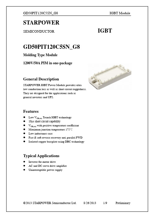
GD50PIT120C5SN_G8
Units
V
A A
Characteristics Values
Symbol VF Qr IRM Erec
Parameter Diode Forward Vol tage
Recovered Charge
Peak Reverse Recovery Current Reverse Recovery Energy
Symbol
VRRM
IF IFRM
Description Repetitive Peak Reverse Voltage @ Tj=25℃ DC Forward Current Repetitive Peak Forward Current tp=1ms
GD50PIT120C5SN_G8
1200
50 100
Features
Low VCE(sat) Trench IGBT technology 10μs short circuit capability VCE(sat) with positive temperature coefficient Maximum junction temperature 175℃ Low inductance case Fast & soft reverse recovery anti-parallel FWD Isolated copper baseplate using DBC technology
Test Conditions
IF=50A,VGE=0V
Tj=25℃ Tj=125℃
Tj=25℃
IF=50A, VR=600V,
Tj=125℃ Tj=25℃
RG=15Ω, VGE=-15V
Tj=125℃ Tj=25℃
英飞凌 PMG1-S0 EZ-PD PMG1第一代PD微控制器 数据表

请注意赛普拉斯已正式并入英飞凌科技公司。
此封面页之后的文件标注有“赛普拉斯”的文件即该产品为此公司最初开发的。
请注意作为英飞凌产品组合的部分,英飞凌将继续为新的及现有客户提供该产品。
文件内容的连续性事实是英飞凌提供如下产品作为英飞凌产品组合的部分不会带来对于此文件的任何变更。
未来的变更将在恰当的时候发生,且任何变更将在历史页面记录。
订购零件编号的连续性英飞凌继续支持现有零件编号的使用。
下单时请继续使用数据表中的订购零件编号。
PMG1-S0数据手册第一代供电微控制器PMG1系列概述EZ-PD PMG1 (第一代PD微控制器) 是具有电力传输 (PD) 应用的高电压微处理器成员之一。
这些芯片拥有一个Arm® Cortex®-M0/M0+ CPU、USB-C PD控制器以及模拟和数字外设。
PMG1适用于嵌入式系统,这些系统为高电压USB PD端口提供电源或消耗来自该端口的电源,并利用微控制器提供额外的控制功能。
图1是PMG1系列的细分情况。
图1.PMG1系列细分情况表1介绍了PMG1系列中不同MCU的性能对比。
表1. PMG1系列中不同MCU的性能对比子系统或范围条目PMG1-S0PMG1-S1PMG1-S2PMG1-S3*CPU和存储器子系统内核ARM Cortex-M0 ARM Cortex-M0 ARM Cortex-M0 Arm Cortex-M0+最大频率 (MHz)48484848 Flash (KB)64 128128256 SRAM (KB)812832供电供电端口11148-QFN具有一个端口97-BGA具有两个端口功能灌电流DRP DRP DRPMOSFET栅极驱动器1x PFET2x PFET2x NFET灵活的2x NFET 故障保护VBUS OVP和UVPVBUS OVP, UVP和OCP。
SCP和RCP (仅适用于发送源配置)。
VBUS, OVP, UVP和OCPVBUS OVP, UVP和OCP。
HY5PS1G1631CFP-S5中文资料
This document is a general product description and is subject to change without notice. Hynix Semiconductor does not assume any responsibility for use of circuits described. No patent licenses are implied.Rev. 0.2 / Dec 20061HY5PS1G431C(L)FP HY5PS1G831C(L)FP HY5PS1G1631C(L)FP1Gb DDR2 SDRAMHY5PS1G431C(L)FP HY5PS1G831C(L)FP HY5PS1G1631C(L)FPRev. 0.2 /Dec 20062Revision DetailsRev.HistoryDraft Date 0.1Initial data sheet released Nov. 20060.2IDD Values addedDec. 2006Rev. 0.2 / Dec 20063Contents1. Description1.1 Device Features and Ordering Information1.1.1 Key Φεατυρεσ1.1.2 Ordering Information 1.1.3 Ordering Frequency 1.2 Pin configuration 1.3 Pin Description2. Maximum DC ratings2.1 Absolute Maximum DC Ratings 2.2 Operating Temperature Condition3. AC & DC Operating Conditions3.1 DC Operating Conditions5.1.1 Recommended DC Operating Conditions(SSTL_1.8)5.1.2 ODT DC Electrical Characteristics 3.2 DC & AC Logic Input Levels3.2.1 Input DC Logic Level 3.2.2 Input AC Logic Level 3.2.3 AC Input Test Conditions 3.2.4 Differential Input AC Logic Level 3.2.5 Differential AC output parameters 3.3 Output Buffer Levels3.3.1 Output AC Test Conditions 3.3.2 Output DC Current Drive 3.3.3 OCD default χηαραχτεριστιχσ3.4 IDD Specifications & Measurement Conditions 3.5 Input/Output Capacitance4. AC Timing Specifications5. Package DimensionsRev. 0.2 /Dec 200641.1 Device Features & Ordering Information1.1.1 Key Features•VDD = 1.8V +/- 0.1V •VDDQ = 1.8V +/- 0.1V•All inputs and outputs are compatible with SSTL_18 interface •8 banks•Fully differential clock inputs (CK, /CK) operation •Double data rate interface•Source synchronous-data transaction aligned to bidirectional data strobe (DQS, DQS)•Differential Data Strobe (DQS, DQS)•Data outputs on DQS, DQS edges when read (edged DQ)•Data inputs on DQS centers when write(centered DQ)•On chip DLL align DQ, DQS and DQS transition with CK transition•DM mask write data-in at the both rising and falling edges of the data strobe•All addresses and control inputs except data, data strobes and data masks latched on the rising edges of the clock •Programmable CAS latency 3, 4, 5 and 6 supported•Programmable additive latency 0, 1, 2, 3, 4 and 5 supported•Programmable burst length 4/8 with both nibble sequential and interleave mode •Internal eight bank operations with single pulsed RAS •Auto refresh and self refresh supported •tRAS lockout supported •8K refresh cycles /64ms•JEDEC standard 60ball FBGA(x4/x8) , 84ball FBGA(x16)•Full strength driver option controlled by EMRS •On Die Termination supported•Off Chip Driver Impedance Adjustment supported •Read Data Strobe supported (x8 only)•Self-Refresh High Temperature EntryOrdering InformationPart No.Configuration PackageHY5PS1G431C(L)FP-XX*256Mx460 BallHY5PS1G831C(L)FP-XX*128Mx8HY5PS1G1631C(L)FP-XX*64Mx1684 Ball Operating FrequencyGrade tCK(ns)CL tRCD tRP Unit E35333Clk C4 3.75444Clk Y53555Clk S52.5555ClkNote:-XX* is the speed bin, refer to the Operation Frequency table for complete Part No.1. DescriptionRev. 0.2 /Dec 200651.2 Pin Configuration & Address Table256Mx4 DDR2 Pin Configuration (Top view: see balls through package)ROW AND COLUMN ADDRESS TABLEITEMS 256Mx4# of Bank 8Bank Address BA0,BA1,BA2Auto Precharge FlagA10/AP Row Address A0 - A13Column AddressA0-A9, A11Page size1 KBVSS DM VDDQ DQ3VSS WE BA1A1A5A9NCNC VSSQ DQ1VSSQ VREF CKEBA0A10A3A7A12VDD NC VDDQ NC VDDLBA2VSS VDD A B C D E F G H J K VSSQ DQS VDDQ DQ2VSSDL RAS CAS A2A6A11NCDQS VSSQ DQ0VSSQ CK CK CS A0A4A8A13VDDQ NC VDDQ NC VDD ODTVDDVSSL321789Rev. 0.2 /Dec 20066128Mx8 DDR2 PIN CONFIGURATION (Top view: see balls through package)ROW AND COLUMN ADDRESS TABLEITEMS 128Mx8# of Bank 8Bank Address BA0, BA1, BA2Auto Precharge FlagA10/AP Row Address A0 - A13Column AddressA0-A9Page size1 KBVSS DM/RDQS VDDQ DQ3VSS WE BA1A1A5A9NCNU/RDQS VSSQ DQ1VSSQ VREF CKEBA0A10A3A7A12VDD DQ6VDDQ DQ4VDDLBA2VSS VDD A B C D E F G H J K VSSQ DQS VDDQ DQ2VSSDL RAS CAS A2A6A11NCDQS VSSQ DQ0VSSQ CK CK CS A0A4A8A13VDDQ DQ7VDDQ DQ5VDD ODTVDDVSSL321789Rev. 0.2 /Dec 2006764Mx16 DDR2 PIN CONFIGURATION (Top view: see balls through package)ROW AND COLUMN ADDRESS TABLEITEMS 64Mx16# of Bank 8Bank Address BA0, BA1, BA2Auto Precharge FlagA10/AP Row Address A0 - A12Column AddressA0-A9Page size2 KB3VSS UDM VDDQ DQ11VSS WE BA1A1A5A9NC, A142NC VSSQ DQ9VSSQ VREF CKEBA0A10/APA3A7A121VDD DQ14VDDQ DQ12VDDLNC, BA2VSS VDD A F G H J K L M 7VSSQ UDQS VDDQ DQ10VSSDL RAS CAS A2A6A11NC, A158UDQS VSSQ DQ8VSSQ CK CK CS A0A4A8NC, A139VDDQ DQ15VDDQ DQ13VDD ODTVDDVSSVSS LDM VDDQ DQ3NC VSSQ DQ1VSSQ VDD DQ6VDDQ DQ4B C D E VSSQ LDQS VDDQ DQ2LDQS VSSQ DQ0VSSQ VDDQ DQ7VDDQ DQ5N P RRev. 0.2 /Dec 20068IDD Test Conditions(IDD values are for full operating range of Voltage and Temperature, Notes 1-5)SymbolConditionsUnits IDD0Operating one bank active-precharge current ; t CK = t CK(IDD), t RC = t RC(IDD), t RAS = t RAS min(IDD) ; CKE is HIGH, CS is HIGH between valid commands;Address bus inputs are SWITCHING;Data bus inputs are SWITCHINGmAIDD1Operating one bank active-read-precharge current ; IOUT = 0mA;BL = 4, CL = CL(IDD), AL = 0; t CK = t CK(IDD), t RC = t RC (IDD), t RAS = t RASmin(IDD), t RCD = t RCD(IDD) ; CKE is HIGH, CS is HIGH between valid commands ; Address bus inputs are SWITCHING ; Data pattern is same as IDD4WmAIDD2P Precharge power-down current ; All banks idle ; t CK = t CK(IDD) ; CKE is LOW ; Other control and address bus inputs are STABLE; Data bus inputs are FLOATINGmAIDD2Q Precharge quiet standby current ;All banks idle; t CK = t CK(IDD);CKE is HIGH, CS is HIGH; Other control and address bus inputs are STABLE; Data bus inputs are FLOATINGmAIDD2N Precharge standby current ; All banks idle; t CK = t CK(IDD); CKE is HIGH, CS is HIGH; Other control and address bus inputs are SWITCHING; Data bus inputs are SWITCHINGmA IDD3PActive power-down current ; All banks open; t CK = t CK(IDD); CKE is LOW; Other control and address bus inputs are STABLE; Data bus inputs are FLOATING Fast PDN Exit MRS(12) = 0mA Slow PDN Exit MRS(12) = 1mAIDD3N Active standby current ; All banks open; t CK = t CK(IDD), t RAS = t RASmax(IDD), t RP=t RP(IDD); CKE is HIGH, CS is HIGH between valid commands; Other control and address bus inputs are SWITCHING; Data bus inputs are SWITCHINGmAIDD4W Operating burst write current ; All banks open, Continuous burst writes; BL = 4, CL = CL(IDD), AL = 0; t CK = t CK(IDD), t RAS = t RASmax(IDD), t RP = t RP(IDD); CKE is HIGH, CS is HIGHbetween valid commands; Address bus inputs are SWITCHING; Data bus inputs are SWITCHING mAIDD4R Operating burst read current ; All banks open, Continuous burst reads, IOUT = 0mA; BL = 4, CL = CL(IDD), AL = 0; t CK = t CK(IDD), t RAS = t RASmax(IDD), t RP = t RP(IDD); CKE is HIGH, CS is HIGH between valid commands; Address bus inputs are SWITCHING;; Data pattern is same as IDD4WmAIDD5BBurst refresh current ; t CK = t CK(IDD); Refresh command at every t RFC(IDD) interval; CKE is HIGH, CS is HIGH between valid commands; Other control and address bus inputs are SWITCH-ING; Data bus inputs are SWITCHINGmAIDD6Self refresh current ; CK and CK at 0V; CKE £ 0.2V; Other control and address bus inputs are FLOATING; Data bus inputs are FLOATINGmAIDD7Operating bank interleave read current ; All bank interleaving reads, IOUT = 0mA; BL = 4, CL = CL(IDD), AL = t RCD(IDD)-1*t CK(IDD); t CK = t CK(IDD), t RC = t RC(IDD), t RRD = t RRD(IDD), t RCD = 1*t CK(IDD); CKE is HIGH, CS is HIGH between valid commands; Address bus inputs are STABLE during DESELECTs; Data pattern is same as IDD4R; - Refer to the following page for detailed timing conditionsmARev. 0.2 /Dec 20069Note:1.VDDQ = 1.8 +/- 0.1V ; VDD = 1.8 +/- 0.1V (exclusively VDDQ = 1.9 +/- 0.1V ; VDD = 1.9 +/- 0.1V for C3 speed grade)2.IDD specifications are tested after the device is properly initialized3.Input slew rate is specified by AC Parametric Test Condition4.IDD parameters are specified with ODT disabled.5.Data bus consists of DQ, DM, DQS, DQS, RDQS, RDQS, LDQS, LDQS, UDQS, and UDQS. IDD values must be met with all combinations of EMRS bits 10 and 11.6.Definitions for IDDLOW is defined as Vin £ VILAC(max)HIGH is defined as Vin Š VIHAC(min)STABLE is defined as inputs stable at a HIGH or LOW level FLOATING is defined as inputs at VREF = VDDQ/2SWITCHING is defined as: inputs changing between HIGH and LOW every other clock cycle (once per two clocks)for address and control signals, and inputs changing between HIGH and LOW every other data transfer (once per clock)for DQ signals not including masks or strobes.Rev. 0.2 /Dec 2006102. Maximum DC Ratings2.1 Absolute Maximum DC RatingsNote:1.Stresses greater than those listed under “Absolute Maximum Ratings” may cause permanent damage to the device. This is a stress rating only and functional operation of the device at these or any other conditions above those indicated in the operational sections of this specification is not implied. Exposure to absolute maximum rat-ing conditions for extended periods may affect reliability.2.Storage Temperature is the case surface temperature on the χεντερ/top side of the DRAM. For the measurement conditions. please refer to JESD51-2 standard.2.2 Operating Temperature ConditionNote:1.Operating Temperature is the case surface temperature on the center/top side of the DRAM. For the measure-ment conditions, please refer to JESD51-2 standard.2.At 85~95° T OPER , Double refresh rate(tREFI:3.9us) is required, and to enter the self refresh mode at this tem-perature range, an EMRS command is required to change ιnternal refresh rate.Symbol ParameterRating Units Notes VDD Voltage on VDD pin relative to Vss - 1.0 V ~ 2.3 V V 1VDDQ Voltage on VDDQ pin relative to Vss - 0.5 V ~ 2.3 V V 1VDDLVoltage on VDDL pin relative to Vss- 0.5 V ~ 2.3 V V 1V IN, V OUT Voltage on any pin relative to Vss - 0.5 V ~ 2.3 V V1T STG Storage Temperature-55 to +100°C 1, 2 I I Input leakage current; any input 0V VIN VDD; all other balls not under test = 0V)-2 uA ~ 2 uA uA I OZOutput leakage current; 0V VOUT VDDQ; DQ and ODT disabled-5 uA ~ 5 uAuASymbol Parameter Rating UnitsNotesT OPER Operating Temperature0 to 95°C 1,2Rev. 0.2 /Dec 2006113. AC & DC Operating Conditions3.1 DC Operating Conditions3.1.1 Recommended DC Operating Conditions (SSTL_1.8)Note:1.Min. Typ. and Max. values increase by 100mV for C3(DDR2-533 3-3-3) speed option.2.VDDQ tracks with VDD,VDDL tracks with VDD. AC parameters are measured with VDD,VDDQ and VDD.3.The value of VREF may be selected by the user to provide optimum noise margin in the system. Typically the value of VREF is expected to be about 0.5 x VDDQ of the transmitting device and VREF is expected to track varia-tions in VDDQ4.Peak to peak ac noise on VREF may not exceed +/-2% VREF (dc).5.VTT of transmitting device must track VREF of receiving device.3.1.2 ODT DC electrical characteristicsNote :1.Test condition for Rtt measurementsMeasurement Definition for Rtt(eff):Apply V IH (ac) and V IL (ac) to test pin separately, then measure current I(V IH (ac)) and I(V IL (ac)) respectively. V IH (ac), V IL (ac), and VDDQ values defined in SSTL_18Measurement Definition for VM :Measurement Voltage at test pin(mid point) with no load.Symbol ParameterRatingUnits Notes Min.Typ. Max.VDD Supply Voltage 1.7 1.8 1.9V 1VDDL Supply Voltage for DLL 1.7 1.8 1.9V 1,2VDDQ Supply Voltage for Output 1.7 1.8 1.9V 1,2VREF Input Reference Voltage 0.49*VDDQ 0.50*VDDQ 0.51*VDDQ mV 3,4VTT Termination VoltageVREF-0.04VREFVREF+0.04V5PARAMETER/CONDITIONSYMBOL MIN NOM MAX UNITS NOTES Rtt effective impedance value for EMRS(A6,A2)=0,1; 75 ohm Rtt1(eff)607590ohm 1Rtt effective impedance value for EMRS(A6,A2)=1,0; 150 ohm Rtt2(eff)120150180ohm 1Rtt effective impedance value for EMRS(A6,A2)=1,1; 50 ohm Rtt3(eff)405060ohm 1Deviation of VM with respect to VDDQ/2delta VM-6+6%1Rtt(eff) =V IH (ac) - V IL (ac)I(V IH (ac)) - I(V IL (ac))delta VM =2 x VmVDDQx 100%- 1Rev. 0.2 /Dec 2006123.2 DC & AC Logic Input Levels3.2.1 Input DC Logic Level3.2.2 Input AC Logic Level3.2.3 AC Input Test ConditionsNote:1.Input waveform timing is referenced to the input signal crossing through the V REF level applied to the device under test.2.The input signal minimum slew rate is to be maintained over the range from V REF to V IH(ac) min for rising edges and the range from V REF to V IL(ac) max for falling edges as shown in the figure below.3.AC timings are referenced with input waveforms switching from VIL(ac) to VIH(ac) on the positive transitions and VIH(ac) to VIL(ac) on the negative transitions.Symbol Parameter Min.Max.Units NotesV IH (dc)dc input logic high VREF + 0.125VDDQ + 0.3V V IL (dc)dc input logic low- 0.3VREF - 0.125VSymbol ParameterDDR2 400,533DDR2 667,800Units NotesMin.Max.Min.Max.V IH (ac)ac input logic high VREF + 0.250-VREF + 0.200-V V IL (ac)ac input logic low-VREF - 0.250-VREF - 0.200VSymbol Condition Value Units Notes V REF Input reference voltage0.5 * V DDQV 1V SWING(MAX)Input signal maximum peak to peak swing1.0V 1SLEW Input signal minimum slew rate1.0V/ns2, 3Rev. 0.2 /Dec 2006133.2.4 Differential Input AC logic LevelNote:1.VIN(DC) specifies the allowable DC execution of each input of differential pair such as CK, CK, DQS, DQS, LDQS,LDQS, UDQS and UDQS.2.VID(DC) specifies the input differential voltage |VTR -VCP | required for switching, where VTR is the true input (such as CK, DQS, LDQS or UDQS) level and VCP is the complementary input (such as CK, DQS, LDQS or UDQS) level.The minimum value is equal to VIH(DC) - V IL(DC).Note:1.VID(AC) specifies the input differential voltage |VTR -VCP | required for switching, where VTR is the true input sig-nal(such as CK, DQS, LDQS or UDQS) and VCP is the complementary input signal (such as CK, DQS, LDQS or UDQS). The minimum value is equal to V IH(AC) - V IL(AC).2.The typical value of VIX(AC) is expected to be about 0.5 * VDDQ of the transmitting device and VIX(AC) isexpected to track variations in VDDQ. VIX(AC) indicates the voltage at which differential input signals must cross.3.2.5 Differential AC output parametersNote:1.The typical value of VOX(AC) is expected to be about 0.5 * V DDQ of the transmitting device and VOX(AC) is expected to track variations in VDDQ. VOX(AC) indicates the voltage at ωηιχη differential output signals must cross.Symbol ParameterMin.Max.Units Notes V ID (ac)ac differential input voltage 0.5VDDQ + 0.6V 1V IX (ac)ac differential cross point voltage0.5 * VDDQ - 0.1750.5 * VDDQ + 0.175V2Symbol ParameterMin.Max.Units Notes V OX (ac)ac differential cross point voltage0.5 * VDDQ - 0.1250.5 * VDDQ + 0.125V1V DDQCrossing pointV SSQV TR V CPV IDV IX or V OX< Differential signal levels >Rev. 0.2 /Dec 2006143.3 Output Buffer Characteristics3.3.1 Output AC Test ConditionsNote:1.The VDDQ of the device under test is referenced.3.3.2 Output DC Current DriveNote:1.V DDQ = 1.7 V; V OUT = 1420 mV. (V OUT - V DDQ )/I OH must be less than 21 ohm for values of V OUT between V DDQand V DDQ - 280 mV.2.V DDQ = 1.7 V; V OUT = 280 mV. V OUT /I OL must be less than 21 ohm for values of V OUT between 0 V and 280 mV.3.The dc value of V REF applied to the receiving device is set to V TT4.The values of I OH(dc) and I OL(dc) are based on the conditions given in Notes 1 and 2. They are used to test device drive current capability to ensure V IH min plus a noise margin and V IL max minus a noise margin are delivered to an SSTL_18 receiver. The actual current values are derived by shifting the desired driver operating point (see Section 3.3) along a 21 ohm load line to define a convenient driver current for measurement.Symbol ParameterSSTL_18 Class IIUnits Notes V OTR Output Timing Measurement Reference Level0.5 * V DDQV1Symbol ParameterSSTl_18Units Notes I OH(dc)Output Minimum Source DC Current - 13.4mA 1, 3, 4I OL(dc)Output Minimum Sink DC Current13.4mA2, 3, 4Rev. 0.2 /Dec 2006153.3.3 OCD default characteristicsNote :1.Absolute Specifications ( Toper; VDD = +1.8V ±0.1V , VDDQ = +1.8V ±0.1V)2.Impedance measurement condition for output source dc current: VDDQ=1.7V; VOUT=1420mV; (VOUT-VDDQ)/Ioh must be less than 23.4 ohms for values of VOUT between VDDQ and VDDQ-280mV.Impedance measurement condition for output sink dc current: VDDQ = 1.7V; VOUT = 280mV; VOUT/Iol must be less than 23.4 ohms for values of VOUT between 0V and 280mV .3.Mismatch is absolute value between pull-up and pull-dn, both are measured at same temperature and voltage.4.Slew rate measured from vil(ac) to vih(ac).5.The absolute value of the slew rate as measured from DC to DC is equal to or greater than the slew rate as measured from AC to AC. This is guaranteed by design and characterization.6.This represents the step size when the OCD is near 18 ohms at nominal conditions across all processcorners/variations and represents only the DRAM uncertainty. A 0 ohm value(no calibration) can only be achieved if the OCD impedance is 18 ohms +/- 0.75 ohms under nominal conditions.Output Slew rate load:7.DRAM output slew rate specification applies to 400, 533 and 667 MT/s speed bins.8.Timing skew due to DRAM output slew rate mis-match between DQS / DQS and associated DQs is included in tDQSQ and tQHS specification.DescriptionParameter Min Nom Max Unit Notes Output impedance---ohms 1Output impedance step size for OCD calibration 0 1.5ohms 6Pull-up and pull-down mismatch 04ohms 1,2,3Output slew rate Sout 1.5-5V/ns1,4,5,6,7,8Rev. 0.2 /Dec 200616IDD Specifications(max)SymbolDDR2 400DDR2 533DDR2 667DDR2 800Unitsx4x8x4x8x16x4x8x16x4x8x16IDD06060656585707090757595mA IDD17070757511080801158585120mA IDD2P 88888888888mA IDD2Q 2222272727303030323232mA IDD2N 3030353535404040454545mA IDD3PF 2020202020252525252525mA S99999999999mA IDD3N 3535454545505050555555mA IDD4W 100100125125160150150195170170225mA IDD4R 100100125125160150150195170170225mA IDD5165165165165165175175175175175175mA IDD6Normal88888888888mA Low power 55555555555mA IDD7165165175175260180180265185185270mA3.4 IDD Specifications & Test ConditionsRev. 0.2 /Dec 200617IDD Test Conditions(IDD values are for full operating range of Voltage and Temperature, Notes 1-5)Symbol ConditionsUnits IDD0Operating one bank active-precharge current ; t CK = t CK(IDD), t RC = t RC(IDD), t RAS = t RAS min(IDD) ; CKE is HIGH, CS is HIGH between valid commands;Address bus inputs are SWITCH-ING;Data bus inputs are SWITCHINGmAIDD1Operating one bank active-read-precharge χυρρεντ ; IOUT = 0mA;BL = 4, CL = CL(IDD), AL = 0; t CK = t CK(IDD), t RC = t RC (IDD), t RAS = t RASmin(IDD), t RCD = t RCD(IDD) ; CKE is HIGH, CS is HIGH between valid commands ; Address bus inputs are SWITCHING ; Data pattern is same as IDD4WmAIDD2P Precharge power-down current ; All banks idle ; t CK = t CK(IDD) ; CKE is LOW ; Other control and address bus inputs are STABLE; Data bus inputs are FLOATINGmA IDD2Q Precharge quiet standby current ;All banks idle; t CK = t CK(IDD);CKE is HIGH, CS is HIGH; Other control and address bus inputs are STABLE; Data bus inputs are FLOATINGmA IDD2NPrecharge standby current ; All banks idle; t CK = t CK(IDD); CKE is HIGH, CS is HIGH; Other control and address bus inputs are SWITCHING; Data bus inputs are SWITCHINGmA IDD3PActive power-down current ; All banks open; t CK = t CK(IDD); CKE is LOW; Other control and address bus inputs are STABLE; Data bus inputs are FLOATING Fast PDN Exit MRS(12) = 0mA Slow PDN Exit MRS(12) = 1mAIDD3N Active standby current ; All banks open; t CK = t CK(IDD), t RAS = t RASmax(IDD), t RP=t RP(IDD); CKE is HIGH, CS is HIGH between valid commands; Other control and address bus inputs are SWITCHING; Data bus inputs are SWITCHINGmAIDD4W Operating burst write current ; All banks open, Continuous burst writes; BL = 4, CL = CL(IDD), AL = 0; t CK = t CK(IDD), t RAS = t RASmax(IDD), t RP = t RP(IDD); CKE is HIGH, CS is HIGH between valid commands; Address bus inputs are SWITCHING; Data bus inputs are SWITCHINGmAIDD4R Operating burst read current ; All banks open, Continuous burst reads, IOUT = 0mA; BL = 4, CL = CL(IDD), AL = 0; t CK = t CK(IDD), t RAS = t RASmax(IDD), t RP = t RP(IDD); CKE is HIGH, CS is HIGH between valid commands; Address bus inputs are SWITCHING;; Data pattern is same as IDD4WmAIDD5BBurst refresh current ; t CK = t CK(IDD); Refresh command at every t RFC(IDD) interval; CKE is HIGH, CS is HIGH between valid commands; Other control and address bus inputs are SWITCH-ING; Data bus inputs are SWITCHINGmAIDD6Self refresh current ; CK and CK at 0V; CKE £ 0.2V; Other control and address bus inputs are FLOATING; Data bus inputs are FLOATINGmAFLOATING is defined as inputs at VREF = VDDQ/2SWITCHING is defined as: inputs changing between HIGH and LOW every other clock cycle (once per two clocks) for address and control signals, and inputs changing between HIGH and LOW every other data transfer (once per clock) for DQ signals not including masks or strobes.IDD7Operating bank interleave read current ; All bank interleaving reads, IOUT = 0mA; BL = 4, CL = CL(IDD), AL = t RCD(IDD)-1*t CK(IDD); t CK = t CK(IDD), t RC = t RC(IDD), t RRD = t RRD(IDD), t RCD = 1*t CK(IDD); CKE is HIGH, CS is HIGH between valid commands; Address bus inputs are STABLE during DESELECTs; Data pattern is same as IDD4R; - Refer to the following page for detailed timing conditionsmARev. 0.2 /Dec 200618Note :1.VDDQ = 1.8 +/- 0.1V ; VDD = 1.8 +/- 0.1V (exclusively VDDQ = 1.9 +/- 0.1V ; VDD = 1.9 +/- 0.1V for C3 speed grade)2.IDD specifications are tested after the device is properly initialized3.Input slew rate is specified by AC Parametric Test Condition4.IDD parameters are specified with ODT disabled.5.Data bus consists of DQ, DM, DQS, DQS, RDQS, RDQS, LDQS, LDQS, UDQS, and UDQS. IDD values must be met with all combinations of EMRS bits 10 and 11.6.Definitions for IDDLOW is defined as Vin £ VILAC(max)HIGH is defined as Vin Š VIHAC(min)STABLE is defined as inputs stable at a HIGH or LOW level FLOATING is defined as inputs at VREF = VDDQ/2SWITCHING is defined as: inputs changing between HIGH and LOW every other clock cycle (once per two clocks)for address and control signals, and inputs changing between HIGH and LOW every other data transfer (once per clock) for DQ signals not including masks or strobes.Rev. 0.2 /Dec 200619For purposes of IDD testing, the following parameters are to be utilizedDetailed IDD7The detailed timings are shown below for IDD7. Changes will be required if timing parameter changes are made to the specification.Legend: A = Active; RA = Read with Autoprecharge; D = DeselectIDD7: Operating Current: All Bank Interleave Read operationAll banks are being interleaved at minimum t RC(IDD) without violating t RRD(IDD) using a burst length of 4. Control and address bus inputs are STABLE during DESELECTs. IOUT = 0mA Timing Patterns for 4 bank devices x4/ x8/ x16-DDR2-400 4/4/4: A0 RA0 A1 RA1 A2 RA2 A3 RA3 D D D D D -DDR2-400 3/3/3: A0 RA0 A1 RA1 A2 RA2 A3 RA3 D D D D-DDR2-533 5/4/4: A0 RA0 D A1 RA1 D A2 RA2 D A3 RA3 D D D D D -DDR2-533 4/4/4: A0 RA0 D A1 RA1 D A2 RA2 D A3 RA3 D D D D DTiming Patterns for 8 bank devices x4/8-DDR2-400 all bins: A0 RA0 A1 RA1 A2 RA2 A3 RA3 A4 RA4 A5 RA5 A6 RA6 A7 RA7-DDR2-533 all bins: A0 RA0 A1 RA1 A2 RA2 A3 RA3 D D A4 RA4 A5 RA5 A6 RA6 A7 RA7 D D Timing Patterns for 8 bank devices x16-DDR2-400 all bins: A0 RA0 A1 RA1 A2 RA2 A3 RA3 D D A4 RA4 A5 RA5 A6 RA6 A7 RA7 D D-DDR2-533 all bins: A0 RA0 D A1 RA1 D A2 RA2 D A3 RA3 D D D A4 RA4 D A5 D A6 RA6 D A7 RA7 D D DDDR2-800DDR2-667DDR2-533DDR2-400Parameter 5-5-56-6-65-5-54-4-43-3-3Units CL(IDD)56543tCK t RCD(IDD)12.515151515ns t RC(IDD)57.560606055ns t RRD(IDD)-x4/x87.57.57.57.57.5ns t RRD(IDD)-x161010101010ns t CK(IDD) 2.5 2.53 3.755ns t RASmin(IDD)4545454540ns t RASmax(IDD)7000070000700007000070000ns t RP(IDD)12.515151515ns t RFC(IDD)-256Mb 7575757575ns t RFC(IDD)-512Mb 105105105105105ns t RFC(IDD)-1Gb 127.5127.5127.5127.5127.5ns t RFC(IDD)-2Gb197.5197.5197.5197.5197.5nsRev. 0.2 /Dec 2006203.5. Input/Output Capacitance4. Electrical Characteristics & AC Timing Specification( 0 ϒ⊃ ϒℜ T CASE ϒℜ 95ϒ⊃; V DDQ = 1.8 V +/- 0.1V; V DD = 1.8V +/- 0.1V)Refresh Parameters by Device DensityDDR2 SDRAM speed bins and tRCD, tRP and tRC for corresponding binNote 1: 8 bank device Precharge All Allowance : tRP for a Precharge All command for an 8 Bank device will equal totRP+1*tCK, where tRP are the values for a single bank Πρεχηαργε, which are shown in the table above.Parameter Symbol DDR2 400DDR2 533DDR2 667DDR2 800UnitsMinMax Min Max Input capacitance, CK and CK CCK 1.0 2.0 1.0 2.0pF Input capacitance delta, CK and CK CDCK x 0.25x 0.25pF Input capacitance, all other input-only pins CI 1.0 2.0 1.0 2.0pF Input capacitance delta, all other input-only pins CDI x 0.25x 0.25pF Input/output capacitance, DQ, DM, DQS, DQS CIO 2.5 4.0 2.5 3.5pF Input/output capacitance delta, DQ, DM, DQS, DQSCDIOx0.5x0.5pFParameterSymbol 256Mb 512Mb 1Gb 2Gb 4Gb Units Refresh to Active/Refresh commandtime tRFC75105127.5195327.5ns Average periodic refresh intervaltREFI0 ϒ⊃ϒℜT CASE ϒℜ 95ϒ⊃7.87.87.87.87.8ns 85ϒ⊃≤…T CASE ϒℜ 95ϒ⊃3.93.93.93.93.9nsSpeed DDR2-800DDR2-667DDR2-533DDR2-400UnitsBin(CL-tRCD-tRP)5-5-56-6-64-4-45-5-54-4-43-3-3Parameter min min min min min min CAS Latency564543tCK tRCD 12.51512151515ns tRP Note112.51512151515ns tRAS 454545454540ns tRC57.56057606055nsRev. 0.2 /Dec 200621Timing Parameters by Speed GradeParameterSymbolDDR2-400DDR2-533UnitNoteminmaxminmaxDQ output access time from CK/CK tAC -600+600-500+500ps DQS output access time from CK/CK tDQSCK -500+500-450+450ps CK high-level width tCH 0.450.550.450.55tCK CK low-level width tCL 0.450.550.450.55tCK CK half period tHP min(tCL,tCH)-min(tCL,tCH)-ps 11,12Clock cycle time, CL=xtCK 5000800037508000ps 15DQ and DM input setup time(differential strobe)tDS(base)150-100-ps 6,7,8,20DQ and DM input hold time(differential strobe)tDH(base)275-225-ps 6,7,8,21DQ and DM input setup time(single ended strobe)tDS 25--25-ps 6,7,8,20DQ and DM input hold time(single ended strobe)tDH 25--25-ps 6,7,8,21Control & Address input pulse width for each inputtIPW 0.6-0.6-tCK DQ and DM input pulse width for each input tDIPW 0.35-0.35-tCK Data-out high-impedance time from CK/CK tHZ -tAC max -tAC max ps 18DQS low-impedance time from CK/CK tLZ (DQS)tAC min tAC max tAC min tAC max ps 18DQ low-impedance time from CK/CK tLZ (DQ)2*tAC mintAC max 2*tAC mintAC max ps 18DQS-DQ skew for DQS and associated DQ signalstDQSQ -350-300ps 13DQ hold skew factortQHS -450-400ps 12DQ/DQS output hold time from DQStQH tHP - tQHS -tHP - tQHS -ps Write command to first DQS latching transition tDQSS WL - 0.25WL + 0.25WL - 0.25WL + 0.25tCK DQS input high pulse width tDQSH 0.35-0.35-tCK DQS input low pulse width tDQSL 0.35-0.35-tCK DQS falling edge to CK setup time tDSS 0.2-0.2-tCK DQS falling edge hold time from CK tDSH 0.2-0.2-tCK Mode register set command cycle time tMRD 2-2-tCK Write postamble tWPST 0.40.60.40.6tCK 10Write preambletWPRE 0.35-0.35-tCK Address and control input setup time tIS 350-250-ps 5,7,9,23Address and control input hold time tIH 475-375-ps 5,7,9,23Read preamble tRPRE 0.9 1.10.9 1.1tCK Read postambletRPST0.40.60.40.6tCK Active to active command period for 1KB page size products (x4, x8)tRRD 7.5-7.5-ns4Active to active command period for 2KB page size products (x16)tRRD10-10-ns 4。
OPF500,OPF510,OPF505,OPF512,OPF507, 规格书,Datasheet 资料

Fea tures•Interfaces with all logic circuits •Two output options•Optimized for fiber optic applicationsusing 50 to 200 micron fiber •Data rate to 200kbps NRZ•Available with multiple packaging optionsDe scrip tionThe OPF500, OPF510 series receivercontains a monolithic integrated circuit which incorporates a photodiode, a linear amplifier, a voltage regulator, and a Schmitt trigger on a single silicon chip.These receivers are designed for short haul fiber optic systems using 850 nm LED’s such as Optek’s OPF300 series.These devices feature TTL\LSTTLcompatible logic level output. An internal voltage regulator allows operation with supply voltages ranging from 4.5V to 16V.Ab so lute Maxi mum Rat ings (T A = 25o C un l ess oth er wise noted)Sup ply Volt a ge ................................................... 18 V Stor a ge Tem p era t ure Range .............................. -65o C to +100o C Op e r a t i ng Tem p era t ure Range ............................. -40o C to +85o C Lead Sol d er i ng Tem p era t ure [1/16 inch (1.6 mm) from case for 5 sec. with sol d er i ng iron].......................................................... 240o C Power Dis s i p a t ion .............................................. 200 mW Du r a t ion of Out p ut Short to V CC ..................................... 1 sec.Volt a ge at Out p ut.................................................. 30 V Sink i ng Cur r ent.................................................. 16 mASche mat icsProd uct Bul le tin OPF500Feb ru ary 1996200kbps Fi ber Op t ic Re ceiverType OPF500, OPF510 Se riesCCCCOUTBuffer/10K PUInverter/10K PUElec tri cal Char ac ter is tics (-40o C to +85o C un l ess oth er wise noted)SYM B OL PA RAME TER MIN TYP MAX UNITS TEST CON DI TIONS V CC Operating Supply Voltage 4.516.0VP IN Input Sensitivity (OPF5X0,1,2) 1.0 1.5µW50% Duty Cycle Square Wave P IN Input Sensitivity (OPF5X5,6,7) 1.5 2.0µW50% Duty Cycle Square WaveV OH High Level Output VoltageBuffer 10K Pull-upV CC -1.5V P IN> 2.0 µW, V CC = 4.5 V to 16 VInverter 10K Pull-up V CC -1.5V PIN< 0.1 µW, V CC = 4.5 V to 16 VV OL Low Level Output VoltageBuffer, 10K Pull-upBuffer Open-collector0.4VP IN< 0.1 µW, V CC = 4.5 V to 16 VInverter, 10K Pull-upInverter Open-collector0.4V P IN> 2.0 µW, V CC = 4.5 V to 16 VI CC Supply Current 5.012.0mA V CC = 4.5 V to 16 V, No load on output BW Bandwidth200kHz P IN> 2.0 µW, 50% Duty CyclePWD Pulse With Distortion10% 1 µW < P IN< 100 µW,f = 20 kHz, D.C. = 50%t r Buffer300ns PIN = 1.5 µW, V CC = 5 V t f100nst r Inverter100ns PIN= 1.5 µW, V CC = 5 V t f300nsPART NUMBER GUIDEOPF5XXOptek Fiber Optic ComponentReceiver0 - Plastic TO-18 Hsg.1 - Plastic TO-18 in SMA2 - Plastic TO-18 in ST*5 - Metal TO-46 Hsg.6 - Metal TO-46 in SMA7 - Metal TO-46 in ST0 - 200kbps, 10K Pull-up buffer (non-inverting) output1 - 200kbps, 10K Pull-up inverting output*ST is a registered trade mark of AT&T.Optek reserves the right to make changes at any time in order to improve design and to supply the best product possible.Typi cal Per form ance CurvesHigh Level Output Voltage vs Ambient TemperatureT A - Ambient Temperature - o C High Level Output Current vs Ambient TemperatureT A - Ambient Temperature - o CLow Level Output Voltage vsAmbient TemperatureT A - Ambient Temperature - o CPlas tic Pack a ge OPF500, OPF510Her metic Pack a ge OPF505, OPF515SMA Pack a ge OPF501, OPF511OPF506, OPF516ST* Pack a ge OPF502, OPF512OPF507, OPF517Op t ek re s erves the right to make changes at any time in or d er to im prove de s ign and to sup p ly the best prod uct pos s i b le.GNDOUTV CCGNDOUTV CCV CCOUTGNDV CCOUTGND。
RD5.1S中文资料

Reverse Current IR (µA)
MAX.
VR (V)
2
30
2
33
2
36
1
39
1
43
0.2
47
0.2
52
0.2
57
0.2
63
0.2
69
0.2
76
0.2
84
0.2
91
4
Data Sheet D11444EJ3V0DS00
RD2.0S to RD120S
TYPICAL CHARACTERISTICS (TA = 25 °C)
DATA SHEET
ZENER DIODES
RD2.0S to RD120S
ZENER DIODES 200 mW 2 PINS SUPER MINI MOLD
DESCRIPTION Type RD2.0S to RD120S Series are 2 PIN Super Mini
Mold Package zener diodes possessing an allowable power dissipation of 200 mW.
Zener Voltage Vz (V)Note 1
MAX.
Iz (mA)
2.20
5
2.40
5
2.60
5
2.90
5
2.75
2.90
3.20
5
3.05
3.20
3.50
5
3.35
3.50
3.80
5
3.65
3.80
4.10
5
3.97
4.10
4.49
WKP101MCPEB0KR;WKP101MCPED0KR;WKP101MCPTG0KR;WKP101MCPSLRKR;WKP331MCPED0KR;中文规格书,Datasheet资料

Document Number: 22206For technical questions, contact: slcap@Revision: 08-Feb-101Ceramic AC CapacitorsClass X1, 760 V AC /Class Y1, 500 V ACWKPVishay DraloricNoteImpedance (Z) as a function of frequency (f) at T a = 20 °C (average).Measurement with lead length 6 mm.DESIGNDisc capacitors with epoxy coatingRATED VOLTAGE U R(X1):760 V AC , 50 Hz (IEC 60384-14.2)(Y1): 500 V AC , 50 Hz (IEC 60384-14.2)250 V AC , 60 Hz (UL1414, CSA C22.2)DIELECTRIC STRENGTH BETWEEN LEADSComponent test:4000 V AC , 50 Hz, 2 sAs repeated test admissible only once with: 3600 V AC , 50 Hz, 2 sRandom sampling test (destructive test):4000 V AC , 50 Hz, 60 sDIELECTRIC STRENGTH OF BODY INSULATION4000 V AC , 50 Hz, 60 s (destructive test)DISSIPATION FACTOR tan δ≤ 25 x 10-3INSULATION RESISTANCE R IS≥ 10 x 109 ΩCATEGORY TEMPERATURE RANGE ϑA(- 40 to + 125) °CCLIMATIC CATEGORY ACC. TO EN60068-140/125/21COATINGEpoxy dipped, insulating, flame retarding acc. to UL 94V-0TAPING AND SPECIAL LEAD CONFIGURATIONSOn requestMARKINGWKP 33 pF to 1.5 nFWKP 2.2 nF to 4.7 nFNote• All approval marks are also shown on the label.760 500 250 ~WKPVishay DraloricCeramic AC CapacitorsClass X1, 760 V AC /Class Y1, 500 V AC For technical questions, contact: slcap@Document Number: 222062Revision: 08-Feb-10Notes(1) Standard lead configuration, other lead spacing and diameter available on request.(2) Capacitance values from 470 pF to 4700 pF: The alternative usage of smaller VKP series is recommended for new application.ORDERING INFORMATION, CERAMIC X1/Y1 CAPACITORS WKPCAPACITANCE (2)(pF)TOL.(%) D x s (mm) F ± 1 (1)(mm) d ± 0.05 (1)(mm)V ± 0.5 (1)(mm)ORDERING CODECLASS 1N 75033± 10 , ± 20 8.0 x 6.012.50.6 1.9WKP330 CP KR CLASS 2K 120047± 10 , ± 20 8.0 x 6.012.50.6 2.3WKP470 CP KR68WKP680 CP KR CLASS 2K 1500100± 10 , ± 20 8.0 x 6.012.50.6 2.3WKP101 CP KR CLASS 2K 2000150± 10 , ± 20 8.0 x 6.012.50.6 2.3WKP151 CP KR220WKP221 CP KR CLASS 2K 4000330± 10 , ± 20 8.0 x 6.012.50.6 2.5WKP331 CP KR470WKP471 CP KR6809.0 x 6.0WKP681 CP KR 100010.0 x 6.00.8 2.7WKP102 CP KR150012.0 x 6.0WKP152 CPKR220013.0 x 6.0WKP222 CP KR330015.0 x 6.0WKP332 CP KR 390016.0 x 6.0WKP392 CP KR 470018.0 x 6.0WKP472 CP KR ORDERING CODE7th digit Capacitance Tolerance:± 10 % = K ± 20 % = M10th to 12th digit Lead Configuration (see General Information)R14th digitRoHS Compliant ComponentAPPROVALSIEC 60384 - 14 / 2nd Issue (1993) incl. Am. 1 (1995) - Safety Tests EN 132 400 (1994) - Safety TestsTHAT APPROVAL TOGETHER WITH THE CB TEST CERTIFICATE SUBSTITUTES THE NATIONAL APPROVAL OF THE FOLLOWING Belgium France Italy Austria China Japan Spain Denmark Greece Luxembourg Portugal Singapore Poland United Germany Ireland Netherlands Sweden Slovenia Hungaria Czech Republic Finland Iceland Norway Switzerland Korea IsraelY1 - Capacitor: CB-T est Certificate:X1 - Capacitor: CB-T est Certificate:DE-1-11002-A1DE-1-11002-A133 pF ... 4.7 nF 33 pF ... 4.7 nF500 V AC 760 V ACMinimum thickness of insulation: 0.4 mmUNDERWRITERS LABORATORIES INC.UL 1414Across-the-line, Antenna-coupling and Line-by-pass component.33 pF ... 4.7 nF250 V ACAgency Files / LicencesE 183 844 V1 S1CANADIAN STANDARDS ASSOCIATION CSA C22.2Across-the-line, antenna-coupling and line-by-pass component 33 pF ... 4.7 nF250 V ACNO 1-98Agency Files / LicencesE 183 844 V1 S1ORDERING INFORMATIONWKP 221M CP ED0K R SERIESCAP. VALUETOLERANCERATED VOLTAGELEADCONFIGURATIONINTERNAL CODEROHS COMPLIANTLegal Disclaimer Notice VishayDisclaimerALL PRODU CT, PRODU CT SPECIFICATIONS AND DATA ARE SU BJECT TO CHANGE WITHOU T NOTICE TO IMPROVE RELIABILITY, FUNCTION OR DESIGN OR OTHERWISE.Vishay Intertechnology, Inc., its affiliates, agents, and employees, and all persons acting on its or their behalf (collectively,“Vishay”), disclaim any and all liability for any errors, inaccuracies or incompleteness contained in any datasheet or in any other disclosure relating to any product.Vishay makes no warranty, representation or guarantee regarding the suitability of the products for any particular purpose or the continuing production of any product. To the maximum extent permitted by applicable law, Vishay disclaims (i) any and all liability arising out of the application or use of any product, (ii) any and all liability, including without limitation special, consequential or incidental damages, and (iii) any and all implied warranties, including warranties of fitness for particular purpose, non-infringement and merchantability.Statements regarding the suitability of products for certain types of applications are based on Vishay’s knowledge of typical requirements that are often placed on Vishay products in generic applications. Such statements are not binding statements about the suitability of products for a particular application. It is the customer’s responsibility to validate that a particular product with the properties described in the product specification is suitable for use in a particular application. Parameters provided in datasheets and/or specifications may vary in different applications and performance may vary over time. All operating parameters, including typical parameters, must be validated for each customer application by the customer’s technical experts. Product specifications do not expand or otherwise modify Vishay’s terms and conditions of purchase, including but not limited to the warranty expressed therein.Except as expressly indicated in writing, Vishay products are not designed for use in medical, life-saving, or life-sustaining applications or for any other application in which the failure of the Vishay product could result in personal injury or death. Customers using or selling Vishay products not expressly indicated for use in such applications do so at their own risk and agree to fully indemnify and hold Vishay and its distributors harmless from and against any and all claims, liabilities, expenses and damages arising or resulting in connection with such use or sale, including attorneys fees, even if such claim alleges that Vishay or its distributor was negligent regarding the design or manufacture of the part. Please contact authorized Vishay personnel to obtain written terms and conditions regarding products designed for such applications.No license, express or implied, by estoppel or otherwise, to any intellectual property rights is granted by this document or by any conduct of Vishay. Product names and markings noted herein may be trademarks of their respective owners.Material Category PolicyVishay Intertechnology, Inc. hereb y certifies that all its products that are identified as RoHS-Compliant fulfill the definitions and restrictions defined under Directive 2011/65/EU of The European Parliament and of the Council of June 8, 2011 on the restriction of the use of certain hazardous substances in electrical and electronic equipment (EEE) - recast, unless otherwise specified as non-compliant.Please note that some Vishay documentation may still make reference to RoHS Directive 2002/95/EC. We confirm that all the products identified as being compliant to Directive 2002/95/EC conform to Directive 2011/65/EU.Revision: 12-Mar-121Document Number: 91000分销商库存信息:VISHAY-BC-COMPONENTSWKP101MCPEB0KR WKP101MCPED0KR WKP101MCPTG0KR WKP101MCPSLRKR WKP331MCPED0KR WKP101MCPDF0KR WKP101MCPEF0KR WKP101MCPERUKR WKP101MCPQG0KR WKP151MCPDF0KR WKP151MCPEB0KR WKP151MCPEF0KR WKP151MCPERUKR WKP330MCPDF0KR WKP330MCPDRUKR WKP330MCPEF0KR WKP470MCPDF0KR WKP470MCPDRUKR WKP470MCPEF0KR WKP680MCPDF0KR WKP680MCPEF0KR WKP471MCPED0KR WKP221MCPDRUKR WKP221MCPED0KR WKP221MCPEF0KR WKP221MCPEFGKR WKP331MCPDF0KR WKP331MCPEF0KR WKP331MCPQG0KR WKP331MCPTE0KR WKP471MCPEF0KR WKP471MCPEFGKR WKP471MCPNZ0KR WKP471MCPSARKR WKP471MCPSVNKR WKP101KCPED0KR WKP101MCPERZKR WKP470MCPERZKR WKP681MCPDF0KR WKP681MCPEF0KR WKP681MCPEJ0KR WKP681MCPQG0KR WKP221MCPERUKR WKP221MCPERZKR WKP331MCPDRUKR WKP331MCPERUKR WKP331MCPERZKR WKP101KCPDF0KR WKP101KCPEF0KR WKP151KCPEF0KR WKP680KCPDF0KR WKP221KCPED0KR WKP221KCPERUKR WKP331KCPEF0KR WKP471MCPDF0KR WKP471MCPDRUKR WKP471MCPERUKR WKP102KCPED0KR WKP681MCPERUKR WKP681MCPERZKR WKP102MCPEH0KR WKP102MCPKX0KR WKP470KCPEF0KR WKP221KCPEF0KR WKP102MCPDF0KR WKP102MCPED0KR WKP102MCPEF0KR WKP102MCPEJ0KR WKP102MCPPA0KR WKP102MCPTH0KR WKP102MCPSAQKR WKP102MCPSUXKR WKP681KCPEJ0KR WKP102MCPDJ0KR WKP102MCPDRTKR WKP102MCPDRUKR WKP102MCPEJGKR WKP102MCPEJXKR WKP102MCPERTKR WKP102MCPERUKR WKP102MCPERYKR WKP102MCPRNAKR WKP102MCPSRKKR WKP152MCPEH0KR WKP152MCPEHNKR WKP152MCPQG0KR WKP152MCPTH0KR WKP102KCPEF0KR WKP152MCPEF0KR WKP152MCPEJ0KR WKP152MCPERUKR WKP152MCPERYKR WKP222MCPEH0KR WKP222MCPKX0KR WKP222MCPNV0KR WKP222MCPNZ0KR WKP222MCPQH0KR WKP222MCPTH0KR WKP222MCPSUXKR WKP222MCPDF0KR WKP222MCPDJ0KR WKP222MCPEF0KR WKP222MCPEJ0KR WKP222MCPEJGKR WKP222MCPEJXKR WKP222MCPSKQKR WKP222KCPQH0KR WKP222KCPEF0KR WKP102MCPERZKR WKP332MCPEH0KR WKP332MCPKX0KR WKP332MCPPK0KR WKP332MCPTH0KR WKP332MCPSLQKR WKP332MCPSUTKR WKP332MCPDF0KR WKP332MCPDJ0KR WKP332MCPEF0KR WKP332MCPEJ0KR WKP332MCPERUKR WKP332MCPSRKKR WKP472MCPDRUAR WKP472MCPERUAR。
INA201AQDGKRQ1;中文规格书,Datasheet资料
DESCRIPTION
The INA200-Q1, INA201-Q1, and INA202-Q1 are high-side current-shunt monitors with voltage output. The INA200-Q1–INA202-Q1 can sense drops across shunts at common-mode voltages from –16V to 80V. The INA200-Q1–INA202-Q1 are available with three output voltage scales: 20V/V, 50V/V, and 100V/V, with up to 500kHz bandwidth.
Copyright © 2011, Texas Instruments Incorporated
/
INA200-Q1 INA201-Q1 INA202-Q1
SBOS558 – APRIL 2011
This integrated circuit can be damaged by ESD. Texas Instruments recommends that all integrated circuits be handled with appropriate precautions. Failure to observe proper handling and installation procedures can cause damage.
The INA200-Q1, INA201-Q1, and INA202-Q1 also incorporate an open-drain comparator and internal reference providing a 0.6V threshold. External dividers are used to set the current trip point. The comparator includes a latching capability, which can be made transparent by grounding (or leaving open) the RESET pin.
TPS51200中文资料
VEN = 3.3 V
VREFOUT = 1.25 V (DDR1), IO = 0 A
VVOSNS
Output DC voltage, VO
1
Please be aware that an important notice concerning availability, standard warranty, and use in critical applications of Texas Instruments semiconductor products and disclaimers thereto appears at the end of this data sheet. PowerPAD is a trademark of Texas Instruments.
TPS51200
SLUS812 – FEBRUARY 2008
ELECTRICAL CHARACTERISTICS
Over recommended free-air temperature range, VVIN = 3.3 V,VVLDOIN = 1.8 V, VREFIN = 0.9 V, VVOSNS = 0.9 V, VEN = VVIN, COUT = 3 × 10 µF and circuit shown in Section 1. (unless otherwise noted)
TW9992_Preliminary_Datasheet_v0.1
TW9992
Ordering Information
PART NUMBER (NOTE 0) TW9992AT-NA1-GR TW9992AT-NA1-GRT
NOTE:
PART MARKING TW9992AT NA1-GR TW9992 NA1-CR
PACKAGE (Pb-Free) 32L WQFN 32 WQFN
YIN0 / YIN0+
YIN3 / YIN2-
SDAT 26
32
31
30
29
28
VSS
27
VDDA VSSA DIAG1 YIN4 / YIN4+ YIN5 / YIN4DIAG2 YIN6 / YIN6+ YIN7 / YIN6-
1 2 3 4 5 6 7 8 10 11 12 13 14 15 16 9
Techwell
PRELIMINARY
Low Power NTSC/PAL/SECAM Video Decoder with Differential CVBS Inputs MIPI-CSI2 Output Interface
THIS IS A PRE-DEVELOPMENT PRELIMINARY DATASHEET. DEVICE FUNCTIONALITY AND SPECIFICATIONS ARE SUBJECT TO CHANGE
PKG. DWG. #
These Intersil Pb-free plastic packaged products employ special Pb-free material sets, molding compounds/die attach materials, and 100% matte tin plate plus anneal (e3 termination finish, which is RoHS compliant and compatible with both SnPb and Pb-free soldering operations). Intersil Pb-free products are MSL classified at Pb-free peak reflow temperatures that meet or exceed the Pb-free requirements of IPC/JEDEC J STD-020.
G591 datasheet V2.0
JRC/CRTGPSModuleHardwareSpecificationThisdocumentspecifiestheelectrical,mechanical,andbehavioralcharacteristicsofJRC/CRTGPSenginemodule.
Module:G591Version:V2.0Date:2008-05-26
DrawnCheckedReleasedRevisionHistoryRevisionReleasedateIssuerChangedescriptionG591V2.02008-4-20CreativeContents1Description...........................................................................................................12Mechanicalspecifications....................................................................................13ElectricalSpecifications.......................................................................................24Typicalcharacteristics..........................................................................................35PinDefinition........................................................................................................46ReferencePCBlayout.........................................................................................67ReferenceDesign................................................................................................78NMEAoutputSentence.......................................................................................99Supplier'sResponsibility....................................................................................1210Noticeforhandling...........................................................................................12AppendixA...........................................................................................................14AppendixB...........................................................................................................15Page1of16