SU学习资料
SU-A29B0中文资料
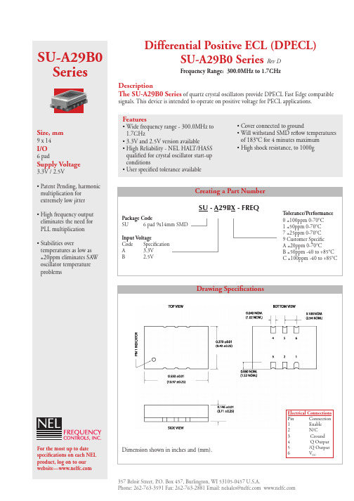
Electrical Connections Pin Connection 1 Enable 2 N/C 3 Ground 4 Q Output 5 /Q Output 6 VCC
357 Beloit Street, P.O. Box 457, Burlington, WI 53105-0457 U.S.A. Phone: 262-763-3591 Fax: 262-763-2881 Email: nelsales@
Creating a Part Number SU - A29BX - FREQ
Package Code SU 6 pad 9x14mm SMD Input Voltage Code Specification A 3.3V B 2.5V Tolerance/Performance 0 ±100ppm 0-70°C 1 ±50ppm 0-70°C 7 ±25ppm 0-70°C 9 Customer Specific A ±20ppm 0-70°C B ±50ppm -40 to +85°C C ±100ppm -40 to +85°C
3.3V / 2.5V • Patent Pending, harmonic multiplication for extremely low jitter • High frequency output eliminates the need for PLL multiplication • Stabilities over temperatures as low as ±20ppm eliminates SAW oscillator temperature problems
Drawing Specifications
For the most up to date specifications on each NEL product, log on to our website—
AT45DB041D-SU-2.5中文资料
Features Array•Single 2.5V or 2.7V to 3.6V Supply•RapidS® Serial Interface: 66 MHz Maximum Clock Frequency–SPI Compatible Modes 0 and 3•User Configurable Page Size–256 Bytes per Page–264 Bytes per Page•Page Program Operation–Intelligent Programming Operation–2,048 Pages (256/264 Bytes/Page) Main Memory•Flexible Erase Options–Page Erase (256 Bytes)–Block Erase (2 Kbytes)–Sector Erase (64 Kbytes)–Chip Erase (4 Mbits)•Two SRAM Data Buffers (256/264 Bytes)–Allows Receiving of Data while Reprogramming the Flash Array•Continuous Read Capability through Entire Array–Ideal for Code Shadowing Applications•Low-power Dissipation–7 mA Active Read Current Typical–25 µA Standby Current Typical–5 µA Deep Power-down Typical•Hardware and Software Data Protection Features–Individual Sector•Sector Lockdown for Secure Code and Data Storage–Individual Sector•Security: 128-byte Security Register–64-byte User Programmable Space–Unique 64-byte Device Identifier•JEDEC Standard Manufacturer and Device ID Read•100,000 Program/Erase Cycles Per Page Minimum•Data Retention – 20 Years•Industrial Temperature Range•Green (Pb/Halide-free/RoHS Compliant) Packaging Options1.DescriptionThe AT45DB041D is a 2.5V or 2.7V, serial-interface Flash memory ideally suited for a wide variety of digital voice-, image-, program code- and data-storage applications. The AT45DB041D supports RapidS serial interface for applications requiring very high speed operations. RapidS serial interface is SPI compatible for frequencies up to 66 MHz. Its 4,325,376 bits of memory are organized as 2,048 pages of 256 bytes or 264 bytes each. In addition to the main memory, the AT45DB041D also contains two SRAM buffers of 256/264 bytes each. The buffers allow the receiving of data while a page in the main Memory is being reprogrammed, as well as writing a continuous data stream. EEPROM emulation (bit or byte alterability) is easily handled with a self-con-tained three step read-modify-write operation. Unlike conventional Flash memories that are accessed randomly with multiple address lines and a parallel interface, the DataFlash uses a RapidS serial interface to sequentially access its data. The simplesequential access dramatically reduces active pin count, facilitates hardware layout,23595H–DFLASH–03/07AT45DB041Dincreases system reliability, minimizes switching noise, and reduces package size. The device is optimized for use in many commercial and industrial applications where high-density, low-pin count, low-voltage and low-power are essential.To allow for simple in-system reprogrammability, the AT45DB041D does not require high input voltages for programming. The device operates from a single power supply, 2.5V to 3.6V or 2.7V to 3.6V, for both the program and read operations. The AT45DB041D is enabled through the Serial Output (SO), and the Serial Clock (SCK).All programming and erase cycles are self-timed.2.Pin Configurations and PinoutsTable 2-1.Pin ConfigurationsSymbolName and FunctionAsserted StateTypeCS Chip Select: Asserting the CS pin selects the device. When the CS pin is deasserted, the device will be deselected and normally be placed in the standby mode (not Deep Power-Down mode), and the output pin (SO) will be in a high-impedance state. When the device is deselected, data will not be accepted on the input pin (SI).A high-to-low transition on the CS pin is required to start an operation, and a low-to-high transition is required to end an operation. When ending an internally self-timed operation such as a program or erase cycle, the device will not enter the standby mode until the completion of the operation.Low InputSCK Serial Clock: This pin is used to provide a clock to the device and is used to control the flow of data to and from the device. Command, address, and input data present on the SI pin is always latched on the rising edge of SCK, while output data on the SO pin is always clocked out on the falling edge of SCK.–InputSI Serial Input: The SI pin is used to shift data into the device. The SI pin is used for all data input includingcommand and address sequences. Data on the SI pin is always latched on the rising edge of SCK. If the SER/BYTE pin is always driven low, the SI pin should be a “no connect”.–InputSO Serial Output: The SO pin is used to shift data out from the device. Data on the SO pin is always clocked out on the falling edge of SCK. If the SER/BYTE pin is always driven low, the SO pin should be a “no connect”.–OutputWPWrite Protect: When the WP pin is asserted, all sectors specified for protection by the Sector Protection Register will be protected against program and erase operations regardless of whether the Enable Sector Protection command has been issued or not. The WP pin functions independently of the software controlled protection method. After the WP pin goes low, the content of the Sector Protection Register cannot be modified.If a program or erase command is issued to the device while the WP pin is asserted, the device will simply ignore the command and perform no operation. The device will return to the idle state once the CS pin has been deasserted. The Enable Sector Protection command and Sector Lockdown command, however, will be recognized by the device when the WP pin is asserted.The WP pin is internally pulled-high and may be left floating if hardware controlled protection will not be used. However, it is recommended that the WP pin also be externally connected to V CC whenever possible.Low InputRESET Reset: A low state on the reset pin (RESET) will terminate the operation in progress and reset the internal state machine to an idle state. The device will remain in the reset condition as long as a low level is present on the RESET pin. Normal operation can resume once the RESET pin is brought back to a high level.The device incorporates an internal power-on reset circuit, so there are no restrictions on the RESET pin during power-on sequences. If this pin and feature are not utilized it is recommended that the RESET pin be driven high externally.Low InputV CC Device Power Supply: The V CC pin is used to supply the source voltage to the device.Operations at invalid V CC voltages may produce spurious results and should not be attempted.–Power GNDGround: The ground reference for the power supply. GND should be connected to the system ground.–Ground33595H–DFLASH–03/07AT45DB041D3.Block DiagramFigure 2-1.MLF Top ViewFigure 2-2.SOIC Top View43595H–DFLASH–03/07AT45DB041D4.Memory ArrayTo provide optimal flexibility, the memory array of the AT45DB041D is divided into three levels of granularity comprising of sectors, blocks, and pages. The “Memory Architecture Diagram” illus-trates the breakdown of each level and details the number of pages per sector and block. All program operations to the DataFlash occur on a page-by-page basis. The erase operations can be performed at the chip, sector, block or page level.Figure 4-1.Memory Architecture Diagram5.Device OperationThe device operation is controlled by instructions from the host processor. The list of instructions and their associated opcodes are contained in Tables 15-1 through 15-7. A valid instruction starts with the falling edge of CS followed by the appropriate 8-bit opcode and the desired buffer loading of the opcode and the desired buffer or main memory address location through the SI (serial input) pin. All instructions, addresses, and data are transferred with the most significant bit (MSB) first.Buffer addressing for the DataFlash standard page size (264 bytes) is referenced in the datasheet using the terminology BEA8 - BFA0 to denote the 9 address bits required to designate a byte address within a buffer. Main memory addressing is referenced using the terminology PA10 - PA0 and BA8 - BA0, where PA10 - PA0 denotes the 11 address bits required to desig-nate a page address and BA8 - BA0 denotes the 9 address bits required to designate a byte address within the page.For the “Power of 2” binary page size (256 bytes), the Buffer addressing is referenced in the datasheet using the conventional terminology BFA7 - BFA0 to denote the 8 address bits required to designate a byte address within a buffer. Main memory addressing is referenced using the terminology A18 - A0, where A18 - A8 denotes the 11 address bits required to desig-nate a page address and A7 - A0 denotes the 8 address bits required to designate a byte address within a page.53595H–DFLASH–03/07AT45DB041D6.Read CommandsBy specifying the appropriate opcode, data can be read from the main memory or from either one of the two SRAM data buffers. The DataFlash supports RapidS protocols for Mode 0 and Mode 3. Please refer to the “Detailed Bit-level Read Timing” diagrams in this datasheet for details on the clock cycle sequences for each mode.6.1Continuous Array Read (Legacy Command – E8H): Up to 66 MHzBy supplying an initial starting address for the main memory array, the Continuous Array Read command can be utilized to sequentially read a continuous stream of data from the device by simply providing a clock signal; no additional addressing information or control signals need to be provided. The DataFlash incorporates an internal address counter that will automatically increment on every clock cycle, allowing one continuous read operation without the need of additional address sequences. To perform a continuous read from the DataFlash standard page size (264 bytes), an opcode of E8H must be clocked into the device followed by three address bytes (which comprise the 24-bit page and byte address sequence) and 4 don’t care bytes. The first 11 bits (PA10-PA0) of the 20-bit address sequence specify which page of the main mem-ory array to read, and the last 9 bits (BA8-BA0) of the 20-bit address sequence specify the starting byte address within the page. To perform a continuous read from the binary page size (256 bytes), the opcode (E8H) must be clocked into the device followed by three address bytes and 4 don’t care bytes. The first 11 bits (A18 - A8) of the 19-bits sequence specify which page of the main memory array to read, and the last 8 bits (A7 - A0) of the 19-bits address sequence specify the starting byte address within the page. The don’t care bytes that follow the address bytes are needed to initialize the read operation. Following the don’t care bytes, additional clock pulses on the SCK pin will result in data being output on the SO (serial output) pin.The CS pin must remain low during the loading of the opcode, the address bytes, the don’t care bytes, and the reading of data. When the end of a page in main memory is reached during a Continuous Array Read, the device will continue reading at the beginning of the next page with no delays incurred during the page boundary crossover (the crossover from the end of one page to the beginning of the next page). When the last bit in the main memory array has been read,the device will continue reading back at the beginning of the first page of memory. As with cross-ing over page boundaries, no delays will be incurred when wrapping around from the end of the array to the beginning of the array.pin (SO). The maximum SCK frequency allowable for the Continuous Array Read is defined by the f CAR1 specification. The Continuous Array Read bypasses both data buffers and leaves the contents of the buffers unchanged.6.2Continuous Array Read (High Frequency Mode – 0BH): Up to 66 MHzThis command can be used with the serial interface to read the main memory array sequentially in high speed mode for any clock frequency up to the maximum specified by f CAR1. To perform a opcode 0BH must be clocked into the device followed by three address bytes and a dummy byte. The first 11 bits (PA10 - PA0) of the 20-bit address sequence specify which page of the main memory array to read, and the last 9 bits (BA8 - BA0) of the 20-bit address sequence spec-ify the starting byte address within the page. To perform a continuous read with the page size set to 256 bytes, the opcode, 0BH, must be clocked into the device followed by three address bytes (A18 - A0) and a dummy byte. Following the dummy byte, additional clock pulses on the SCK pin will result in data being output on the SO (serial output) pin.63595H–DFLASH–03/07AT45DB041DThe CS pin must remain low during the loading of the opcode, the address bytes, and the read-ing of data. When the end of a page in the main memory is reached during a Continuous Array Read, the device will continue reading at the beginning of the next page with no delays incurred during the page boundary crossover (the crossover from the end of one page to the beginning of the next page). When the last bit in the main memory array has been read, the device will con-tinue reading back at the beginning of the first page of memory. As with crossing over page boundaries, no delays will be incurred when wrapping around from the end of the array to the beginning of the array. A low-to-high transition on the CS pin will terminate the read operation and tri-state the output pin (SO). The maximum SCK frequency allowable for the Continuous Array Read is defined by the f CAR1 specification. The Continuous Array Read bypasses both data buffers and leaves the contents of the buffers unchanged.6.3Continuous Array Read (Low Frequency Mode: 03H): Up to 33 MHzThis command can be used with the serial interface to read the main memory array sequentially without a dummy byte up to maximum frequencies specified by f CAR2. To perform a continuous 03H, must be clocked into the device followed by three address bytes (which comprise the 24-bit page and byte address sequence). The first 11 bits (PA10 - PA0) of the 20-bit address sequence specify which page of the main memory array to read, and the last 9 bits (BA8 - BA0) of the 20-bit address sequence specify the starting byte address within the page. To perform a contin-uous read with the page size set to 256 bytes, the opcode, 03H, must be clocked into the device followed by three address bytes (A18 - A0). Following the address bytes, additional clock pulses on the SCK pin will result in data being output on the SO (serial output) pin.The CS pin must remain low during the loading of the opcode, the address bytes, and the read-ing of data. When the end of a page in the main memory is reached during a Continuous Array Read, the device will continue reading at the beginning of the next page with no delays incurred during the page boundary crossover (the crossover from the end of one page to the beginning of the next page). When the last bit in the main memory array has been read, the device will con-tinue reading back at the beginning of the first page of memory. As with crossing over page boundaries, no delays will be incurred when wrapping around from the end of the array to the beginning of the array. A low-to-high transition on the CS pin will terminate the read operation and tri-state the output pin (SO). The Continuous Array Read bypasses both data buffers and leaves the contents of the buffers unchanged.6.4Main Memory Page ReadA main memory page read allows the user to read data directly from any one of the 2,048 pages in the main memory, bypassing both of the data buffers and leaving the contents of the buffers unchanged. To start a page read from the DataFlash standard page size (264 bytes), an opcode of D2H must be clocked into the device followed by three address bytes (which comprise the 24-bit page and byte address sequence) and 4 don’t care bytes. The first 11 bits (PA10-PA0) of the 20-bit address sequence specify the page in main memory to be read, and the last 9 bits (BA8-BA0) of the 20-bit address sequence specify the starting byte address within that page.To start a page read from the binary page size (256 bytes), the opcode D2H must be clocked into the device followed by three address bytes and 4 don’t care bytes. The first 11 bits (A18 - A8) of the 19-bits sequence specify which page of the main memory array to read, and the last 8 bits (A7 - A0) of the 19-bits address sequence specify the starting byte address within the page. The don’t care bytes that follow the address bytes are sent to initialize the read opera-tion. Following the don’t care bytes, additional pulses on SCK result in data being output on the SO (serial output) pin. The CS pin must remain low during the loading of the opcode, the address bytes, the don’t care bytes, and the reading of data. When the end of a page in main73595H–DFLASH–03/07AT45DB041Dmemory is reached, the device will continue reading back at the beginning of the same page. A low-to-high transition on the CS pin will terminate the read operation and tri-state the output pin (SO). The maximum SCK frequency allowable for the Main Memory Page Read is defined by the f SCK specification. The Main Memory Page Read bypasses both data buffers and leaves the contents of the buffers unchanged.6.5Buffer ReadThe SRAM data buffers can be accessed independently from the main memory array, and utiliz-ing the Buffer Read Command allows data to be sequentially read directly from the buffers. Four opcodes, D4H or D1H for buffer 1 and D6H or D3H for buffer 2 can be used for the Buffer Read Command. The use of each opcode depends on the maximum SCK frequency that will be used to read data from the buffer. The D4H and D6H opcode can be used at any SCK frequency up to the maximum specified by f CAR1. The D1H and D3H opcode can be used for lower frequency read operations up to the maximum specified by f CAR2.To perform a buffer read from the DataFlash standard buffer (264 bytes), the opcode must be clocked into the device followed by three address bytes comprised of 15 don’t care bits and 9buffer address bits (BFA8-BFA0). To perform a buffer read from the binary buffer (256 bytes),the opcode must be clocked into the device followed by three address bytes comprised of 16don’t care bits and 8 buffer address bits (BFA7 - BFA0). Following the address bytes, one don’t care byte must be clocked in to initialize the read operation. The CS pin must remain low during the loading of the opcode, the address bytes, the don’t care bytes, and the reading of data. When the end of a buffer is reached, the device will continue reading back at the beginning the output pin (SO).7.Program and Erase Commands7.1Buffer WriteData can be clocked in from the input pin (SI) into either buffer 1 or buffer 2. To load data into the DataFlash standard buffer (264 bytes), a 1-byte opcode, 84H for buffer 1 or 87H for buffer 2,must be clocked into the device, followed by three address bytes comprised of 15 don’t care bits and 9 buffer address bits (BFA8-BFA0). The 9 buffer address bits specify the first byte in the buffer to be written. To load data into the binary buffers (256 bytes each), a 1-byte opcode 84H for buffer 1 or 87H for buffer 2, must be clocked into the device, followed by three address bytes comprised of 16 don’t care bits and 8 buffer address bits (BFA7 - BFA0). The 8 buffer address bits specify the first byte in the buffer to be written. After the last address byte has been clocked into the device, data can then be clocked in on subsequent clock cycles. If the end of the data buffer is reached, the device will wrap around back to the beginning of the buffer. Data will con-7.2Buffer to Main Memory Page Program with Built-in EraseData written into either buffer 1 or buffer 2 can be programmed into the main memory. A 1-byte opcode, 83H for buffer 1 or 86H for buffer 2, must be clocked into the device. For the DataFlash standard page size (264 bytes), the opcode must be followed by three address bytes consist of 4 don’t care bits, 11 page address bits (PA10 - PA0) that specify the page in the main memory to be written and 9 don’t care bits. To perform a buffer to main memory page program with built-in erase for the binary page size (256 bytes), the opcode 83H for buffer 1 or 86H for buffer 2, must be clocked into the device followed by three address bytes consisting of 5 don’t care bits83595H–DFLASH–03/07AT45DB041D11page address bits (A18 - A8) that specify the page in the main memory to be written and 8don’t care bits. When a low-to-high transition occurs on the CS pin, the part will first erase the selected page in main memory (the erased state is a logic 1) and then program the data stored in the buffer into the specified page in main memory. Both the erase and the programming of the page are internally self-timed and should take place in a maximum time of t EP . During this time,the status register will indicate that the part is busy.7.3Buffer to Main Memory Page Program without Built-in EraseA previously-erased page within main memory can be programmed with the contents of either buffer 1 or buffer 2. A 1-byte opcode, 88H for buffer 1 or 89H for buffer 2, must be clocked into the device. For the DataFlash standard page size (264 bytes), the opcode must be followed by three address bytes consist of 4 don’t care bits, 11 page address bits (PA10-PA0) that specify the page in the main memory to be written and 9 don’t care bits. To perform a buffer to main memory page program without built-in erase for the binary page size (256 bytes), the opcode 88H for buffer 1 or 89H for buffer 2, must be clocked into the device followed by three address bytes consisting of 5 don’t care bits, 11 page address bits (A18 - A8) that specify the page in the main memory to be written and 8 don’t care bits. When a low-to-high transition occurs on the CS pin, the part will program the data stored in the buffer into the specified page in the main mem-ory. It is necessary that the page in main memory that is being programmed has been previously erased using one of the erase commands (Page Erase or Block Erase). The programming of the page is internally self-timed and should take place in a maximum time of t P . During this time, the status register will indicate that the part is busy.7.4Page EraseThe Page Erase command can be used to individually erase any page in the main memory array allowing the Buffer to Main Memory Page Program to be utilized at a later time. To perform a page erase in the DataFlash standard page size (264bytes), an opcode of 81H must be loaded into the device, followed by three address bytes comprised of 4 don’t care bits, 11 page address bits (PA10-PA0) that specify the page in the main memory to be erased and 9 don’t care bits.To perform a page erase in the binary page size (256 bytes), the opcode 81H must be loaded into the device, followed by three address bytes consist of 5 don’t care bits, 11 page address bits (A18 - A8) that specify the page in the main memory to be erased and 8 don’t care bits. When a state is a logical 1). The erase operation is internally self-timed and should take place in a maxi-mum time of t PE . During this time, the status register will indicate that the part is busy.7.5Block EraseA block of eight pages can be erased at one time. This command is useful when large amounts of data has to be written into the device. This will avoid using multiple Page Erase Commands.To perform a block erase for the DataFlash standard page size (264bytes), an opcode of 50H must be loaded into the device, followed by three address bytes comprised of 4 don’t care bits,8page address bits (PA10 - PA3) and 12 don’t care bits. The 8 page address bits are used to specify which block of eight pages is to be erased. To perform a block erase for the binary page size (256 bytes), the opcode 50H must be loaded into the device, followed by three address bytes consisting of 5 don’t care bits, 8 page address bits (A18 - A11) and 11 don’t care bits. The 9 page address bits are used to specify which block of eight pages is to be erased. When a low-to-high transition occurs on the CS pin, the part will erase the selected block of eight pages. The erase operation is internally self-timed and should take place in a maximum time of t BE . During this time, the status register will indicate that the part is busy.93595H–DFLASH–03/07AT45DB041D7.6Sector EraseThe Sector Erase command can be used to individually erase any sector in the main memory.There are 8 sectors and only one sector can be erased at one time. To perform sector 0a or sec-tor 0b erase for the DataFlash standard page size (264 bytes), an opcode of 7CH must be loaded into the device, followed by three address bytes comprised of 4 don’t care bits, 8 page address bits (PA10 - PA3) and 12 don’t care bits. To perform a sector 1-7 erase, the opcode 7CH must be loaded into the device, followed by three address bytes comprised of 4 don’t care bits, 3 page address bits (PA10 - PA8) and 17 don’t care bits. To perform sector 0a or sector 0b erase for the binary page size (256 bytes), an opcode of 7CH must be loaded into the device,followed by three address bytes comprised of 5 don’t care bit and 8 page address bits (A18 -A11) and 11 don’t care bits. To perform a sector 1-15 erase, the opcode 7CH must be loaded into the device, followed by three address bytes comprised of 5 don’t care bit and 3 page address bits (A18 - A16) and 17 don’t care bits. The page address bits are used to specify any valid address location within the sector which is to be erased. When a low-to-high transition self-timed and should take place in a maximum time of t SE . During this time, the status register will indicate that the part is busy.Table 7-1.Block Erase AddressingPA10/A18PA9/A17PA8/A16PA7/A15PA6/A14PA5/A13PA4/A12PA3/A11PA2/A10PA1/A9PA0/A8Block 00000000X X X 000000001X X X 100000010X X X 200000011X X X 3••••••••••••••••••••••••••••••••••••11111100X X X 25211111101X X X 25311111110X X X 25411111111XXX255103595H–DFLASH–03/07AT45DB041D7.7Chip Erase (1)The entire main memory can be erased at one time by using the Chip Erase command.To execute the Chip Erase command, a 4-byte command sequence C7H, 94H, 80H and 9AH must be clocked into the device. Since the entire memory array is to be erased, no address bytes need to be clocked into the device, and any data clocked in after the opcode will be ignored. After the last bit of the opcode sequence has been clocked in, the CS pin can be deas-serted to start the erase process. The erase operation is internally self-timed and should take place in a time of t CE . During this time, the Status Register will indicate that the device is busy.The Chip Erase command will not affect sectors that are protected or locked down; the contents of those sectors will remain unchanged. Only those sectors that are not protected or locked down will be erased.The WP pin can be asserted while the device is erasing, but protection will not be activated until the internal erase cycle completes.Figure 7-1.Chip EraseNote: 1.Refer to the errata regarding Chip Erase on page 52.Table 7-2.Sector Erase AddressingPA10/A18PA9/A17PA8/A16PA7/A15PA6/A14PA5/A13PA4/A12PA3/A11PA2/A10PA1/A9PA0/A8Sector 00000000X X X 0a 00000001X X X 0b 001X X X X X X X X 1010X X X X X X X X 2••••••••••••••••••••••••••••••••••••100X X X X X X X X 4101X X X X X X X X 5110X X X X X X X X 6111XXXXXXXX7Command Byte 1Byte 2Byte 3Byte 4Chip EraseC7H94H80H9AHAT45DB041D7.8Main Memory Page Program Through BufferThis operation is a combination of the Buffer Write and Buffer to Main Memory Page Programwith Built-in Erase operations. Data is first clocked into buffer 1 or buffer 2 from the input pin (SI)and then programmed into a specified page in the main memory. To perform a main memorypage program through buffer for the DataFlash standard page size (264 bytes), a 1-byte opcode,82H for buffer 1 or 85H for buffer 2, must first be clocked into the device, followed by threeaddress bytes. The address bytes are comprised of 4 don’t care bits, 11 page address bits,(PA10-PA0) that select the page in the main memory where data is to be written, and 9 bufferaddress bits (BFA8-BFA0) that select the first byte in the buffer to be written. To perform amain memory page program through buffer for the binary page size (256 bytes), the opcode 82Hfor buffer 1 or 85H for buffer 2, must be clocked into the device followed by three address bytesconsisting of 5 don’t care bits, 11 page address bits (A18 - A8) that specify the page in the mainmemory to be written, and 8 buffer address bits (BFA7 - BFA0) that selects the first byte in thebuffer to be written. After all address bytes are clocked in, the part will take data from the inputpins and store it in the specified data buffer. If the end of the buffer is reached, the device willpin, the part will first erase the selected page in main memory to all 1s and then program thedata stored in the buffer into that memory page. Both the erase and the programming of thepage are internally self-timed and should take place in a maximum time of t EP. During this time,the status register will indicate that the part is busy.8.Sector ProtectionTwo protection methods, hardware and software controlled, are provided for protection againstinadvertent or erroneous program and erase cycles. The software controlled method relies onthe use of software commands to enable and disable sector protection while the hardware con-that are to be protected or unprotected against program and erase operations is specified in thenonvolatile Sector Protection Register. The status of whether or not sector protection has beenenabled or disabled by either the software or the hardware controlled methods can be deter-mined by checking the Status Register.。
苗族文字学习资料

TSIAJ NTAWV TXIV(声母)p ph np nphpl plh npl nplhm hm ml hml f vt th nt nth n hnd dh l hltx txh ntx ntxh xts tsh nts ntsh s zr rh nr nrhc ch nc nchny hny xy yk kh nk nkh hq qh nq nqhTSIAJ NTAWV NIAM(韵母)a ai e ee i iao oouua au aw w声调TSIAJ NTAWV CIMb(siab)j (nyuj) v(kuv) d(tod) –(ua) g(neeg) s(muas) m( nyiam)说明:一、苗文的拼音形式有3种:(1)韵母中平调自成音节。
如:i 那里,o 臃肿,w 抛撒。
(2)声母加韵母中平调。
如:zoo 好,li 的,ntau 多。
(3)声母加韵母加声调,如:peb 三,koj 你,ntawv 书。
二、苗文单词在中国有人主张不连写,如:ntoo thuv ;而在国外则主张连写,sawvdaws。
三、苗文大写规则、标点符号与其他拉丁字母形式的文字基本相同。
P paj 花pog 阿婆,祖母peb 三,我们paub 懂,知道pawg 堆,群pw 睡(觉)poob qab 落后pub npua 喂猪puav leej 全体,全部,所有pab 帮,帮助PH phom 炮,枪phawv 顿萝phoom 碰phem 坏ntoo phuam载帕子phooj ywg 朋友phauj 姑妈pheej yig 便宜NP npe 字,名字npuav (口)含npawg 表兄弟npab 手臂npu paj 雪花npaj 办理,操作npau tawg 发火npoj 群,众NPH nphoo 撒(灰)nphav raug 碰着nphoo ntshuas 纷飞、零乱nphau 反转PL plab 肚子ntxuj plig 灵魂plaub 四,毛,事情plaub ntug 事件,案件plawv 心脏pluav 砸,不规则ploj tuag 死亡,消失plauv tshauv 灰尘ib pluag mov 一餐饭ya plawg (突然)飞起PLH plhu 脸,面子plhaws quav 不稳重,轻浮pliaj plhus面貌plhaub qes 蛋壳plhis plaub换毛plhauj taub 葫芦瓢NPL nplej 稻谷nplooj 叶子nplaig 舌头nplua 滑nplua nuj 富裕nplaim tawg 火焰mov nplaum 糯饭plhaub npluag 空壳NPLH nplhaib 戒子ntses nti nplhij nplhoj 鱼翻动的响声Hneev nyuj nplhaus nplhiv 牛脚迹杂乱的样子nplhos riag rau 插刀MMab 彝族,哈尼族Mab suav 指苗族以外的其他民族miv 猫mov 饭mus 去moo 消息,讯息qhov muag 眼睛xov maj 麻线zib mu 蜂糖(蜜糖)HMHmoob 苗族hmuv 刺hma 狼hmo ntuj 夜晚hmaub kev 走夜路hmob qaib 墨蚊sib hmov sib tshua 互相思念,疼爱ML mloog lus 听话tsev mlom 寺庙,庙堂mluav 溢出mluag mlob 精神萎靡HML hmlos 喵Miv quaj hmlawg hmlom 猫吼叫的声音Nyuj tsuj av hmlos zog 牛踩坭深陷Ffaib 分(东西)fwj 壶,瓶子feem 份foom 祝愿fab 翻(东西)fob mov 翻蒸二道包谷面饭fws 汗fub taub 葫芦瓢V vaj 王,(菜)园子voom 犁vauv 女婿vam 希望txhiab vam 千万vov vuag 盖瓦kev vam meej 致富路vej voog 陀螺T tuv 猜,猜测tub rog 军队,兵tw 尾巴taw 脚taus 斧头tooj 铜tag 完,结束tiag 真,垫tuav tes 握手tua tuag 杀死teem caij 定时,约定to taub 明白,理解tab tom 正当,正在tab sis但是tam sis(na)现在TH thoob 桶thiab 同,和,与,跟thov 请,恳求thoj 陶(姓)tham lus 谈话thawj coj 首领,首长,领导thaum ub 从前,古时候NT ntawv 书,文字,信,纸ntaiv 梯子ntaub 布ntau 多ntev 长ntaj 大刀ntuv 砍(树)ntu 吐,砍(南瓜等)ntuj tshiab 春天nto npe 出名,有名ntaub ntawv 知识,文化NTH nthab 楼nthuav 散,翻(书)nthe 骂nthee ncuav 炸粑粑nthias sub pwg 提肩膀N niam 妈noj 吃noog 鸟nab 蛇neeg 人nom tswv 官吏neej tsa 亲戚nws 他nees 马HN hnub 日,太阳hnub qub 星星hneev 印子,弓箭hnoos 咳嗽hnav 芝麻,苏麻hnav tsoos 穿着hnab maj 麻袋kaus hniav 牙齿dev 狗daj 黄色dag 哄,骗dub 黑色dawb 白色daim 块,张dab tsi 什么deev hluas 恋爱dab neeg 故事,传说dob nroj 拔草dav fo 宽敞,宽阔duj 武术DH dhuav (吃)腻,厌烦dhia qeej 跳芦苼舞dhau dua 通过,来往dhau qab (桶底)脱落Lliaj 田,鹞子luv 燕子,短luav 免子,驴子lawv 他们,别人looj leej 隆林ua laj luam 经商,做生意hauj lwm 活路,工作,任务lis piam 礼拜,星期HL hli 月,月亮hluas 青年,年轻hle 脱hlais 割hlau 铁,贼hlub hlav 生长,发展dav hlau 飞机sis hmov sis hlub 互相关爱hluas nkauj hluas nraug 少男少女Tx txiv 爹,果子txoj 条txiaj 钱,货币txawv 不同,差别,差异kua txob 辣椒txuj ci 风俗,知识文,技术ib txwm 一向,一贯,从来txom nyim 可怜,困难raug txim 受治,被惩罚txiag txaj 订板tub txawg 知识分子TXH txha 骨txhuv 米txhaum txwv 锉子txhia leej 各位txhav 僵硬txho tshauv 灰色txhua chaw 各地,各处txheeb ze 亲人txhawb txhim 支持,赞助,帮助NTX ntxab 米ntxuam 扇子ntxiv 补,补充,加,增加ntxub 恨,嫉妒ntxug 锁sawv ntxov 早上,起早nyuam ntxaib 双胞胎ntxeev cev 翻身cheb ntxa ntxhuab 青苔ntxhais ntxawm 小女,公主ntxhua tsho 洗衣toj ntxhab 陡坡ntxhib ntxho 粗糙ntxhov tsoog 零乱X xav 想,思考,考虑xov 信,线xub 先,首先xauv 锁xob quaj 雷鸣xov xwm 消息,信息,报纸tshaj xov 通讯,宣传,广播tshuab tshaj xov 广播电台cawv xeev 生日TS tsov 虎tsa 立,建立tsev 家,房子tseeb 真,争tsim 制,制造,设计tsiaj txhu 牲畜tswv yim 主意tsoog tsho 服装Tsoob kuj 中国ua tsaug 感谢,谢谢ntau tsawg 多少tsim txiaj 值钱,有价值tsis tsiv 不(逃)跑TSH tsheb 车tshuaj 药tshauv 灰tshis 山羊tshais 早饭,三七,漆树Tshuab ntaus ntawv 打字机tshav ntuj 天晴,礼物,恩情扫墓NTXH ntxhw 象paj tshoob kev kos 婚事婚俗tshiab 烤NTS ntsev 盐ntsuas tshuv 孤儿ntsaum 蚂蚁ntsuab 绿色ntseeg 相信,信任tub ntsuag 孤儿neeg ntse 聪明人ntsaj mob(病痛)呻吟txiaj ntsig 恩情,感情Tsis quav ntsej 不理睬NTSH ntshav 血ntshai 怕,恐怕,可能ntshaw 羡慕pag dej ntshiab 清水潭nqaij ntshiv 瘦肉SSuav 汉族sau 写(字),收(东西)siab 心,高se 租,借sov 暖和seev 带感情的哼或唱sawv daws携手,一起sab laj 商量,研究,协议sav yeeb 便宜sib tw 比赛,竞争suab saib qes 声调sov siab 心暖sib tham 互相讨论sib pab 互相帮助sia siv 系腰带Z zog 寨子,村子,力气zaum 坐zeb 石头,石磨zoo 好,佳,妙,良ua zam 打份zaj txuj 文章,作品,著作zaj 龙,节目,行zom zawg 纷纷zoj zees 快速,急忙,赶紧zam txim 原谅,谅解ze chaw 亲戚R raj 笛子rog 兵,肥ris 背,负责rawg 筷子rau 六,(拿)给rooj 桌子ris tsho 衣裤rov qab 返回,回来rau siab 专心,用心raws siab xav 随心所欲,如意rub tes 拉手roj 油roj ci 电池roob 山RH rhawv (水)缸rhais 插rhaub zaub 热菜rheeb kab (鸡)觅虫rho nroj 拔草NR nrov 响nruas 鼓nruab 装(东西)南北nroog 市,城市nruab nrab 中间,中部nraj tiab 点(画)蜡裙nraj duab 画图nra hnyav 背负担重,责任重大sawv nrug/nreg 站立NRH nrhoob 绑腿带nrhiav 找,寻觅nrhab 沾莲子Hlua tu(nrho) 绳子断C ci 亮(光),烧cog 种(庄稼),陷害caij 时间,骑cua 风,啃(骨头)haus cawv 喝酒ntoo ciab 衫树neeg coob 人多cev tes 伸手caj ceg 根源,情况,状况CH choj 桥chij 旗chib 扫cheem 劝(说)chwv raug 摩擦着teb chaws 地方chaws qhov 进洞chob koob 穿针qhov chiv 厕所NC ncaj 直(线)ncej 柱子ncauj 嘴巴ncas 口弦ncuav 粑粑nco ntsoov 牢记,切记,铭记ncaim 分别,分手,离别ncaws pob 踢足球viv ncaus 姐妹,姊妹teg ncees/nceeg teg 手准NCH nchuav 倒(东西)nchos 抖(动)ncho pa 冒烟,蒸汽tsw nchauv嗅侬(焦味)nchav nchav 生硬,僵硬NYnyuj 牛nyab 媳妇nyob 坐,在,住nyiag 偷,各自nyiam 爱nyuam 孩子nyiaj kub 金银nyaj 姑妈HNYhnyav 重hnyuv 肠子kub hnyiab 烧焦(过火)Mus kev tsaj nyaws hnyo 走路不断晃动的样子XYxyoo 年,岁xyab 香(火),伸(手)xyaum 学xyaw 混合,参杂xyeej 闲xyiv fab 喜欢,欢迎xyoob ntoo 竹木xyom cuab 孝家xyem xyav 犹豫,迟疑Y yaj 杨,溶化,自然消失yog 是yuav 要yawg 祖父,阿公yug noog 奍鸟yooj yim 容易yub zaub 菜秧yuam kev 错路,岐途yus tus kheej 本人,本己yaum/yum 约,邀约K koj 你kuv 我kawg 完了,结束,极限kawm 背萝,背篼kwv tij 弟兄kws ntawv 老师kaj siab 舒心,愉快,高兴ntuj kub 热天,夏天ntuj tsaug 冬天ntuj daj 秋天kab xes 磁带(录音,录像)KH khau 鞋子khi 拴khiab 开,付(款)khaws 捡(东西)kiab khws 街道,市场kho/khu mob 治病,医病kho txhim 整顿,治理khoov duav 弯腰,弓背khoom 空闲khoob tes 空手NK nkoj 船nkaj 兰靛nkawd 他俩nkeeg 懒惰,病nkaus 獐子,伞zoo nkauj 漂亮,美丽hu nkauj dhia zaj 唱歌跳舞nkuaj npuas 猪圈nkoog daus 结冰NKH nkhib ntoo 树桠杈nkhib nkhaus 波折,弯路,挫折nkhaus nib nkhaus nob弯弯曲曲nkhis nkhoos 叮咚(象声词)Hho 还,还要hu 喊,叫hais 说,讲Hais lus 说话haus dej 喝水heev 狠,很,厉害hawj 侯(姓)haws 草果huab tais 皇帝hav liaj 田坝huab cua 风云,气候huv si 全体,全部,所有,共计Q qav 蛙qe 蛋qaib 鸡qub 旧,陈旧qauv 尸,尸体qaw 吼叫qoob 粮食qoob loo 庄稼qaum ntuj 天上noj qab nyob zoo 幸福安康ua qauv 做榜样,做示范QH qheb 开qhev 奴隶,佣人,奴婢qhub 辣椒,辣子qhawv 包装qhuas 夸奖,表扬,称赞qha qhuav 烘干qhuab qhia 教育,指导,教导qhov chaw 地点,地址,地方qhov tug 哪里qhov ntuj 天井Haiv Hmoob qhov rais 苗族之窗NQ nqaij 肉nqov (牛)嚎叫nqu 咳嗽nqes 下(去)nquag 勤劳nqa siab 提高nqia duav 细腰nuj nqe 债务nquam khw 赶街nqaus paj nqaus nruag 跳坡娱乐(节日)NQHnqhes dej 渴水Hav zoo nqha nrig茂密的森林SUAB NTA (韵母)Aa 阿av 坭巴,土nas 鼠mag 挟着,中计,被phab 页,边,方(向)phab hnub tuaj 东方zaj 龙,行,首(量词)AIai 唉vai 喂dais 熊txhais 解释,翻译txhaib 饿qaij 歪niam tais 外婆Haiv neeg 民族tog txais 迎接,接待xaiv lus/lus xaiv 谣言AU aub 狗(别名)kaum 十,角(度)pauv 换,交换npau 沸腾haub 哄,骗zaub 菜hau 头,首长,领导qaum teb 北方,涨部,北面qaug 跌倒nkauj ntxhais nraug tub 艳女俊男AW aw 骂(人)caw 请,邀请,邀约kaw 关,锯,锯子kawm ntawv 读书,上学yawg saub 上帝E ev 背(小孩)qev 借(东西)sev 围腰dej 水ntseg 鱼kev hlau 铁路Qhev 仡佬族,奴隶Tsev kawm ntawv 学校EE teeb 灯nqeeb 草yeeb 烟nees 马tseem fwv 政府tseeb cai 真理,科学nyeem zaj txuj 念文章teeb meem 谜语,障碍txheej txheem 程序,顺序,目录yees duab 摄影,照相yeeb yam 电影,音像I ib 一yim 八,亿(数)yiv 壮族,傣族ntim 碗ntsis plaub hau 梳头发sib fem 相会,交流ua qias i 做某件事(不明说)ua si 做玩,玩耍txi txiv 结果IA iab 苦iav 镜子,锈水txiab 剪刀riam 刀liab 猴子,红色liaj teb 田地tsiab tshiab 新年,新春tshav ziab 太阳晒nyiaj txiag 金钱,经费tiav 完了毕业,结束viav viag 千秋,摇篮tiam qhua待客O o 肿(大)ob 二so 休息,擦,抺os 鸭thoj 陶,淘pom 见,看见npoj 群pob 球,包lom zem 闹热,娱乐khov kho 结实,硬朗noj mov 吃饭dawb dawb mos mos 白白嫩嫩OO xyooj 熊(姓)koom xov 针线xov tooj 电话xov tooj cua 无线电,电台zoo mloog 好听noob qoob 农作物种子zoov ntoo 森林foom koov 俸供,祝贺,祝愿koob meej 名誉,地位looj koov 纠缠,吵烦loog 麻木lag loo 城市vaj loog 园子,公园U tub 儿子,深tug 个,只,头,根puv 满nug 问,询问kub 热,黄金zuj zug 逐渐,缓慢nuv/suas ntseg 摸鱼UA ua 做liaj uab 乌鸦zuaj 狐狸xyuam 瞎puav 蝙蝠kua 汤qhua 客人cuaj 九txeeb cuav 真假ua ub ua no 做这做那vam fuaj/fuaj vam发旺,荣繁W w 撒(肥料)ws 鹌鹑wb 我俩kwv 弟,扛(东西)twm 水牛khwv 苦,辛苦lwj 腐烂,碎,粉碎xws 虾xub pwg 肩膀cwj thaig 餐具pob kws 包谷(玉米)kws txuj 作家,专家twb ywm 悄悄地cwj ntawv 纸笔AA(安)qaab 甜,底部xyaa nyuas 生仔(哺乳动物)paab 帮(且),搬(迁)xaa 送,赠maaj 麻,忙kaab 虫,钢qaab teb 南方,南部,南面cwj mem 笔墨。
西班牙语学习资料汇总

语音阶段ALFABETO 字母表字母名称音标字母名称音标A a A [ a ] N n ene [ n, m ]B b be [ b, β ] Ñ ñ eñe []C c ce [ θ, k, γ ] O o o [ o ]Ch ch che [ c ] P p pe [ p ]D d de [ d, ð ] Q q cu [ k ]E e e [ e ] R r ere[ r, ]F f efe [ f ] rr erre[ ]G g ge [ g, γ, x ] S s ese [ s ], [ z ]H h hache 不发音T t te [ t ]I i i [ i ] U u u [ u ]J j jota [ x ] V v uve [ b, β ] K k ca [ k ] W w doble uve [ β ]L l ele [ l ] X x equis [ s, γs ] LL ll elle [ λ ] Y y ye/igriega [ j, i ]M m eme [ m ] Z z zeta/zeda [ θ ]一、元音1. A a 非圆唇低元音2. E e 非圆唇中前元音3. I i 非圆唇高前元音4. O o 圆唇中后元音5. U u 圆唇高后元音二、辅音(一) Ll, Mm, Nn, Pp, Ss, Tt的发音1.L l 发舌尖齿龈边擦浊辅音[ l ]la, le, li, lo, luala, ele, ili, olo, ululelo, lila, Lola, lulúl 在词尾的发音:al, el, il, ol, ul2.M m 发双唇鼻浊辅音[ m ]ma, me, mi, mo, muama, eme, imi, omo, umuEma, mal, lame, melón, mimo, mil, mola, mole, mula3.N n 发舌尖齿龈鼻浊辅音[ n ]na, ne, ni, no, nuana, ene, ini, ono, unumina, luna, nene, Nilo, maní, mano,mono, menú, nulo以n结尾的音节的发音an, en, in, on, unan: canta, trabajanen: mente, momentoin: fin, sin, mintióon: pon, son, tazónun: un melón, mundo4.P p 发双唇塞清辅音[ p ]pa, pe, pi, po, puapa, epe, ipi, opo, upupala, mapa, pena, pelo, pipa, pila, pone, pumapapel, pulpo5.S s 发舌尖齿龈擦清辅音[ s ]sa, se, si, so, suasa, ese, isi, oso, ususano, sala, mesa, seno, sima, asilo, soso,solo, suma, supo, sal, nasals 在词尾的发音:as, es, is, os, usmasas, mesas, salas, osos, somos, sumass 在其他浊辅音之前的发音:asma, asno, isla, mismo6.T t 发舌尖齿背塞清辅音ta, te, ti, to, tuata, ete, iti, oto, ututasa, tala, mete, tipo, timo, tono, moto, tuna, tal, total发音练习:lata, sola, misa, mono, pata, pese, sopa, tomo, sol, alto, limosna, palma(二)Cc, Qq, Dd, Bb, Vv, Rr1.Cc(1)在与a, o, u 构成音节时,发舌后软腭塞清辅音[ k ]。
普通话学习资料

dǎsuɑn
打听
dǎtinɡ
大方
dàfɑnɡ
大爷
dàye
71-75
大夫
dàifu
带子
dàizi
袋子
dàizi
耽搁
dānɡe
耽误
dānwu
76-80
单子
dānzi
胆子
dǎnzi
担子
dànzi
刀子
dāozi
道士
dàoshi
81-85
稻子
dàozi
灯笼
dēnɡlonɡ
提防
dīfɑnɡ
笛子
dízi
底子
dǐzi
媳妇
xífu
喜欢
xǐhuɑn
瞎子
xiāzi
441-445
匣子
xiázi
下巴
xiàbɑ
吓唬
xiàhu
先生
xiānshenɡ
乡下
xiānɡxiɑ
446-450
箱子
xiānɡzi
相声
xiànɡshenɡ
消息
xiāoxi
小伙子
xiǎohuǒzi
小气
xiǎoqi
451-455
小子
xiǎozi
笑话
xiàohuɑ
料子
liàozi
林子
línzi
翎子
línɡzi
256-260
领子
lǐnɡzi
溜达
liūdɑ
聋子
lónɡzi
笼子
lónɡzi
炉子
lúzi
261-265
路子
lùzi
轮子
lúnzi
萝卜
luóbo
部编二年级下册听写与默写汇总(看拼音+古诗课文积累)
tù zi
ān jìnɡ
ɡēn běn
tònɡ kǔ
zuì jìn
shū diàn
jué dìnɡ
nónɡ fū
shānɡ diàn
wán quán zhōnɡ yú
jiāo huàn
rì qī
qīnɡ wā
mǎi mài
bān jiā
dǎo xià
cài zǐ
quán shuǐ
pò huài
yīnɡ ɡāi
zhuǎn yǎn
qīnɡ mínɡ
xiān rén
yuán yuè zhōnɡ qiū
关注微信公众号【统编版语文电子课本】,可领取更多学习资料!
cǎi sè
mènɡ xiǎnɡ
第四单元 sēn lín
lā shǒu
jié ɡuǒ
jiē shi pínɡ ɡuǒ
yì bān
jīnɡ línɡ
yóu xì
日积月累
语文园地一 赋得古原草送别
, , ,
[] 。 。 。
◎予人玫瑰, ◎平时肯帮人, ◎与其锦上添花,
语文园地二 。 。 。
语文园地四
◎
。——《老子》
◎
。 ——《左传(zhu n)》
◎
。——《韩(h n)非子》
语文园地六 悯农(其一)
,
[] 。
关注微信公众号【统编版语文电子课本】,可领取更多学习资料!
chī jīnɡ
jiǎo bù
mínɡ bai
rán hòu mài zi
sì zhōu
wánɡ yánɡ
bǔ láo
jiǎo dù
jīn pí lì jìn
关注微信公众号【统编版语文电子课本】,可领取更多学习资料!
柬语学习资料
挖掘机
e-si-ga
e-si-ga
渣场
工n来嘟万桶噜n给
gon lai do wan to lun gie
自卸车
烂蹬嘚
lan deng dei
营地
当木了探
dang mu le tan
通风机
工哈
gong ha
修理车间
Jong juer贡来特嘎
ju juer gon lai te ga
轻、重
斯然、特un
si ra,te un
洗手间在哪里?
本都蹬nou哪?
bon dom deng nou na
粗、细
咯让、 嘟
ge ra,do
你叫什么名字?
酿七木诶?
niang qi mu ei
下雨、天晴
Pe令、斯岸
pe lieng, si an
我的名字叫阿里。
棵niom 七木阿里
ke niom qi mu a li
钻杆
dong带jo
dong dai jo
办公室
嘎日呀来以
ga ri ya lai
吊车
烂斯嘟
lan si du
试验室
搬动币臊
bon dum bi sao
测量
颗vo
ke vo
(炸药)仓库
颗亮
ke liang dang ga nong
测量仪器
吗信克窝
ma xin ke vo
食堂
pe嗲后吧以
gon lai niam ba yi
mie ga ma go
机油
呗ring吗信
be ring ma xin
劳务
工m浪波了干
Unit5Helpingourparents学习资料(素材)译林版英语五年级下册
Unit 5 Helping our parents【词汇】1.parent父或母2. clean擦,洗3.cook烧,煮4.sweep 扫5.busy 忙碌6.wash 洗7. dish 盘,碟8. grow 种植9. garden花园,果园10.sweet甜的11. pest害虫12. ladybird瓢虫13.breakfast 早餐14.fruit 水果15.grow 生长16.wind风17.blow 吹;打击18.bring带来19.kettle壶20. grape 葡萄21. continued 继续的22. housework家务劳动【词组或短语】1. help our parents 帮助我们的父母2. Saturday morning 星期六上午3. on Saturday morning 在周六早上4. clean the car洗车,擦车5. help him帮助他6. cook breakfast in the kitchen 在厨房做早饭7. cook lunch做午饭8. cook supper 做晚饭9. in the living room在起居室,在客厅里10. sweep the floor 扫地11. in his bedroom 在他的卧室12. in the afternoon在下午13. my cousin Jim我的堂兄弟吉姆(堂兄弟姐妹或表兄弟姐妹) 14. be busy忙的15. cook dinner做晚饭16. help her帮她17.wash the dishes 洗碗,洗盘子18. clean the table擦桌子19. eat fruit in the living room在客厅吃水果20.watch TV看电视21. make the bed整理床铺22. wash clothes 洗衣服23.do some washing 洗衣服24. help their parents 帮助他们的父母25. help his parents 帮助他的父母26. help him with his Maths 帮助他学数学27. watch the flowers growing看着花儿生长28. in the evening在傍晚,在晚上*29. listen to the wind blowing 听风吹(的声音)30. grow grapes种葡萄31.in his garden在他的花园里32. big and sweet 又大又甜32.some pests on the grapes 葡萄上的一些害虫34. eat your grapes 吃你的葡萄35.so sweet如此甜36. some ladybirds一些瓢虫36.go away 走了,离开38. do one’s homework做家庭作业39.do her homework做她的回家作业40. play computer games 玩电脑游戏41. chat on the Internet网上聊天42. play with a toy car玩玩具汽车43. play with his toy car 玩他的玩具汽车44. some housework一些家务*45.put the kettle on 烧壶水【句型】1. It is Saturday morning. 这是周六早上。
天然材料与人造材料(课件)-三年级科学下册(苏教版)
尝试进行分类,说明原因。
活动讲授
什么是天然材料,什么是人造材料
(1)天然材料:直接来自大自然,如木材、石材、棉花 、羊毛等,它们属于天然材料。 (2)人造材料:不是直接来自大自然,而是通过加工处 Lorem ipsum dolor sit amet, consectetuer
全课总结
今天我们一起走进了奇妙的材料世界,通过交流思考造房子和书包里 的材料,以及看一看、摸一摸、浸一浸、烧一烧等方式比较棉花和晴纶棉 等活动,了解天然材料和人造材料、感知到天然材料和人造材料的特性。 同时通过视频,了解到如何将天然材料进行加工,形成人造物,以及使用 天然材料或人造材料多寡的原因,学会树立保护环境资源的观念。
这些材料有什么特点?
活动讲授
区分天然材料和人造材料
同桌交流:你们的发现是否正确,并进行汇报
物品名称 可能使用的材料
Lorem ipsum dolor sit amet, consectetuer adipiscing elit. Aenean commodo ligula eget dolor.
Lorem ipsum dolor sit amet, consectetuer adipiscing elit. Aenean commodo ligula eget dolor.
学习目标
1 通过交流造房子需要哪些材料,观察了解并学会区分 天然材料和人造材料。
通过看一看、摸一摸、浸一浸、烧一烧等方式比较棉 2 花和晴纶棉,发现它们的相似处和不同点,初步感知
比较天然材料和人造材料的异同。
sothat和suchthat区别与练习_2022年学习资料
1.This is-So-interesting a book that we all enjoy rea ing it.-2.This is-s such an i-interesting book that w all enjoy reading it.-3.They are such-interesting bo ks that we all enjoy reading them.-4.He has So-many b oks that I can't count them.-5.This is such a funny s ory that we all enjoy listening to it.-6.There was-SO much food that we couldn't eat it all.-7.I have-littl money that I cannot afford a car.-8.He is-such a goo student that we all like him.-9.He is-good a student that we all like him.-10.It was such bad weather that he had to stay at home.-11.It's not surprising that s ch little worms eat-little grain.
so.that和-such.tha区别与练习so.that和such.that的意思均为“如此...以-致”,都用来引导结果状语丛包。但二者用-法不尽 同,现归纳如下:-1-so.that结构中的so为副词,后面跟形容-词或副词;-such.that中的su h为形容词,-后面接名-词(名词前可以有形容词或副词修饰)。-例如:-●He became/is so a gry that he couldn‘t-speak.-他变得很生气,以致说不出话来-oIt was su h a fine day that we went out for a-walk.
- 1、下载文档前请自行甄别文档内容的完整性,平台不提供额外的编辑、内容补充、找答案等附加服务。
- 2、"仅部分预览"的文档,不可在线预览部分如存在完整性等问题,可反馈申请退款(可完整预览的文档不适用该条件!)。
- 3、如文档侵犯您的权益,请联系客服反馈,我们会尽快为您处理(人工客服工作时间:9:00-18:30)。
网易 新闻 微博 邮箱 闪电邮 相册 有道 手机邮 印像派 梦幻人生
更多 博客 博客首页 博客话题 热点专题 博客油菜地 找朋友 博客圈子 博客风格 手机博客 短信写博 邮件写博 博客复制 摄影 主题展区 每日专题 摄影人物志 摄影师专访 摄影点评 随便看看
晚安日志圣诞版 注册 登录 显示下一条 | 关闭 tset 显示下一条 | 关闭
厚土家园
不在沉默中爆发,就在沉默中死亡!
导航 首页 日志 相册 音乐 收藏 博友 关于我
日志
厚土家园 做规划、建设自己的厚土家园!! 加博友 关注他
最新日志 非常全面的教育网址大全【教 高考前3个月教你从300分提 办公室专用表格--常用的100 爱不释手的资料秘籍网址!! 工作之余,别忘了给自己充电 百万书库精品收藏
博主推荐 相关日志 随机阅读 【原创图文】深宫锁唐妃 何苦冬盼春 东莞豪宅的四个“过度” 不可思议!七种会走路的神奇鱼类 从台湾居民赴欧免签想起了“夺印” 若非异地,怎知你无可代替. 人生感悟:请尊重我的平凡(图)
首页推荐 年度十大性事件评选 有中国特色的网络围观 香车美女惊艳车展 杨澜:主持周立波婚礼 热带雨林里钓食人鱼 在巴西亲密接触水蛇
更多>>
老工程师的CAD精髓
芬兰“海洋魅力”邮轮超“泰坦尼克号”极尽奢华、演绎浪漫!
草图大师 实用信息与知识 2010-10-17 20:55:06 阅读79 评论0 字号:大中小 订阅
这是我自己的一些经验。如果你对su还没有很多的了解和经验,那么试试按照下面说得去做,直到你得出了自己的经验和见解。我采用下面这些方法,是因为它们适合我工作的习惯,其他人可能会有不同的适合自己的方法,如果你有更好的招数,拿出来和大家共享一下子吧!
1. 建模--步骤 首先,一条原则是我们应该尽量将模型量控制在最简单,最小。当然,如果你以建立细致入微的模型为乐趣的话,那么可以不必遵循这个原则。但是,如果你是用su来养家活口,维持生计,那么过分细致的模型是没有必要的。你应该努力在完成工作的前提下,将模型建的尽量简单。一旦你不得不更改模型的时候,尤其是本来即将完成时,需要更改的话,越简单的模型越容易修改。 如果你的模型按照一定的原则清晰的分成了组或组件,那么其实你就可以将任意组件保存成一个单独的文件,在需要改变组件的时候,只需要打开保存的那个文件,进行编辑并保存,然后在含有这个组件的模型中,重新调用就可以了,这样做不必受场景中其他东西的干扰,编辑速度也快。如果你边建模边推敲方案,那么就先建立一个大的体块,随着你设计的深入,逐渐将模型加入细节。你可以轻松的将一些粗糙的大体块替换为精致的模型,当然前提是你要有足够深入的设计。
2. 导入CAD文件 (怎么样处理CAD图的导入,另外可以利用CAD建立的立面图,辅助线工具的利用,组功能的应用还有一些快捷的方式) 将CAD文件导入su,然后通过简单地描一描线段,使它生成面,然后推推拉拉地建立起一个3D模型,这听起来确实令人兴奋。但是这样工作的效果实际上取决于你的CAD图的质量。 导入CAD的2D文件,实际上能产生许多令人头疼的麻烦。熟手画得简单的轮廓线的CAD图不会产生什么大的 麻烦,生手画的细节繁多,杂乱无章的CAD图就不那么容易利用了。“带有小小的线段、转角处两条线没有相交、一条线和另外一条看上去平行实际上只差一点点”,由这些问题的CAD图,都会在你建立模型的时候成为你的绊脚石,似乎应该说是钢针,因为它们小的让你很难察觉和纠正。用这样的CAD图导入su作为底图,你花费在纠正错误上的时间反倒会比你节省的时间多。 接近完成的CAD图纸,实际上包含了大量你建模时用不着的信息。你在CAD制图中过分详细的分层方法或者是重叠的线等等,都是在su中建立模型所不需要的。如果你要用这样一张漏洞百出,复杂无比的CAD图纸导入su来建模,而你在之前要做的清理工作会浪费很多时间。(译者:所以不如在导入su后,马上炸开所有CAD中形成的块,将所有线归到一层,然后将这些变为一个组,作为底图,在它上面重新描一遍会更节省时间)。 即使是进行了良好分层的2D CAD图纸也不是没有问题的。记住:su的层不会为你隔离在不同层的线(也就是说,比如有三条线分属三个层,他们围合成一个面,这个面仍然会产生,而不会因为这三条线不在一个层上而不产生这个面。),su中的层仅仅是在视觉上区分线面的分类方法。这个特性同样适用于导入的CAD图。任何在一个层上的线如果与其他层上的线重合,那么在导入过程中都将被无情地清理掉。所以,在某些时候,一层一层地导入将会非常有用,每导入一个层的东西,su都会将其自动成组,也不会误杀重叠的线(译者:注意这里是说要将CAD中的不同层分别保存到不同的CAD文件,这样做是因为在CAD中关闭不可见的层也会被导入到su中)。 CAD中带有门窗的墙已经被门窗打断,如果你导入这样的CAD图就需要花费时间来补上门窗上下部分的墙面。 立面图作为单独的一个面,通常对于建立3D模型来说不具有多大的意义,但是非常有用的的一点是,你可以将立面图导入后,立起来,放在模型大体块的旁边,用来帮助你准确地捕捉立面上的尺寸。我的经验是:回避潜在的问题,用在SU中重新描画一遍CAD图的方法来代替用导入的CAD图直接拉伸建模式最好的方法。我将导入的CAD图作成组(这样可以防止在SU中画的线面和他们粘在一起),然后描画我需要的线,如果必要的话,简化我描的线(举例来说,忽略开窗墙面上的洞口,我会在稍后插入窗的组件)。我在任何需要和可能的地方使用矩形工具以及捕捉锁定功能。不要轻易相信你捕捉到了角点,就能画出一个漂亮的方形(除非你自己一根线一根线地去画,并且确认你画方形的附近没有讨厌的“短短线”)(译者:老外管这种无用的短短的长度几乎为零的废线叫“哎呀”,呵呵,挺有意思,我下面也这么叫了)。 如果你决定直接用导入的CAD图来拉伸建模,你必须意识到任何怪异的毛病(脱离轴线的线,短线,复线还有“哎呀”等等)都将被导入SU并成为你模型的一部分,你也许仅仅会在某些地方发现它们藏在有用的线的下面,那么准备好开开心心地清理和纠正他们吧。(译者:老外似乎带点威胁的口气,不过大家还是听他的吧,老老实实跟他走) 同时记住,如果你通过拉伸整个平面来建立了模型,那么所有的几何体都将是粘在一起的。这样的模型将很难编辑其中的一部分而不影响其它部分,而且很难在事后将他们分组或组件。(译者:所以大家建立模型的时候,应该随建随把不同的体块分成不同的组或组件) 一些建模的关键 在你成为SU建模的高手之前,关闭“长度捕捉”(一种类似网格捕捉的捕捉。译者:这个开关在WINDOW--MODEL INFO--UNITS--ENABLE LENGTH SNAPPING中控制)除非你必须要用这种捕捉形式捕捉模型中的每个网格点。要善用辅助线工具。多多地用。建立一个一次清除所有辅助线的快捷键,一遍你在场景中充斥辅助线的时候方便地删除他们。辅助线有各种各样的用途。比如你在用一张导入的图片为基础进行建模时:如果你画几条辅助线在图片中一些重要的线上,你就能轻松地够捕捉到一些有用的点。捕捉锁定功能(INFERENCE LOCKING)在有辅助线的时候也能更好地发挥作用。沿着一条辅助线移动物体也比凭空在3D空间中沿一定方向移动物体快得多。 使用尽量少的鼠标点击次数来完成一个任务是我们的主旨。但有些时候,比较快的方法是多画一些东西作为辅助,然后走一小段回头路。比如说,选择一个面的所有边线的快捷方法是,先选择这个面和他的所有边线(这个目的我们可以轻松地通过双击鼠标点击面来达到)然后将面排除出选择,这样比我们一根根地选择边线快得多。像拉伸这样的工具,以及自动折叠功能,还有移动同时复制等可以快速地建立新的几何体,比我们手工去画快得多。尽量在可能的情况下使用这些方法,而不是傻乎乎地去一根根线地画,甚至有些时候通过这些方法产生的几何体会有一些多余的线或面,而你要在事后清理它们,也比你自己画快得多。矩形工具通常比直线工具更加快捷,并且在画方形或闭合四边形的时候有特别的优势。应该试者找寻利用矩形工具画复杂形体的途径,(用两次可以画出"L"形的平面,三次可以画出"H"形的平面等等)然后只要删除一到两条线就可以完成工作,总比你用直线工具费劲地捕捉这里那里画出所有的边线来得快吧。因为SU有独特的霍尼维尔(HEALS)线特性,删除不用的线后,被分割的平面可以自动愈合。 拉伸工具是我们将2D图形变为3D模型的利器,它可以轻松地帮我们建立需要的面。尽量融会贯通地使用这个工具,为了使某些地方可以拉伸,也可以画一些多余的线来达到目的,拉伸,然后删除不想要的面。 说了这么多,大家也要融会贯通,有时候与其你节省5分钟的时间来用所谓的快捷方法建立一个几何体,却用了15分钟来思考怎样“快捷”达到目的,还不如你用画线工具一笔笔画出来强。
3. 捕捉和捕捉锁定 讨厌的鼠标自己跳到一个被捕捉到的点,而给你的建模带来了麻烦?你希望能将这个过分“智能”的捕捉关闭掉,而使你能安安静静地画图吗?非常遗憾,你不能关闭这种捕捉,SU没有这种捕捉就不是SU了,所以还是开心地接受它吧,它是有史以来最好的功能。(译者:老外的话让我想起了一句名言“生活就像是被强奸,如果你无力反抗,那么就好好享受吧”) 下面讲一下,它在画线和移动的时候是怎样工作的: (译者:这一部分我在网站的FLASH教程中有专门的讲解,老外说得和我大同小异,所以不费力翻译出来了,大家看我的教程即可。) 如果你没有捕捉到你想要的方向(特别是轴向),而是捕捉到了其他几何体上的