安捷伦定向耦合器资料
定向耦合器的原理与应用

定向耦合器的原理与应用下载温馨提示:该文档是我店铺精心编制而成,希望大家下载以后,能够帮助大家解决实际的问题。
文档下载后可定制随意修改,请根据实际需要进行相应的调整和使用,谢谢!并且,本店铺为大家提供各种各样类型的实用资料,如教育随笔、日记赏析、句子摘抄、古诗大全、经典美文、话题作文、工作总结、词语解析、文案摘录、其他资料等等,如想了解不同资料格式和写法,敬请关注!Download tips: This document is carefully compiled by the editor. I hope that after you download them, they can help yousolve practical problems. The document can be customized and modified after downloading, please adjust and use it according to actual needs, thank you!In addition, our shop provides you with various types of practical materials, such as educational essays, diary appreciation, sentence excerpts, ancient poems, classic articles, topic composition, work summary, word parsing, copy excerpts,other materials and so on, want to know different data formats and writing methods, please pay attention!定向耦合器是一种广泛应用于微波和射频系统中的关键组件,它能够在系统中实现信号的传输和耦合,发挥着重要的作用。
利用ADS设计超宽带定向正交耦合器的设计与实现_毕业设计论文

题(中、英文)作者姓指导教师姓名、学科门代分类学密Design and Implementation of Ultra WidebandDirectional Quadrature Coupler西安电子科技大学学位论文创新性声明秉承学校严谨的学风和优良的科学道德,本人声明所呈交的论文是我个人在导师指导下进行的研究工作及取得的研究成果。
尽我所知,除了文中特别加以标注和致谢中所罗列的内容以外,论文中不包含其他人已经发表或撰写过的研究成果;也不包含为获得西安电子科技大学或其它教育机构的学位或证书而使用过的材料。
与我一同工作的同志对本研究所做的任何贡献均已在论文中做了明确的说明并表示了谢意。
申请学位论文与资料若有不实之处,本人承担一切的法律责任。
本人签名:日期西安电子科技大学关于论文使用授权的说明本人完全了解西安电子科技大学有关保留和使用学位论文的规定,即:研究生在校攻读学位期间论文工作的知识产权单位属西安电子科技大学。
学校有权保留送交论文的复印件,允许查阅和借阅论文;学校可以公布论文的全部或部分内容,可以允许采用影印、缩印或其它复制手段保存论文。
同时本人保证,毕业后结合学位论文研究课题再撰写的文章一律署名单位为西安电子科技大学。
(保密的论文在解密后遵守此规定)本学位论文属于保密,在年解密后适用本授权书。
本人签名:日期导师签名:日期摘要摘要定向耦合器是能够进行功率分配的射频微波器件,具有广泛的应用。
本文讨论的定向耦合器工作频段为30MHz~512MHz,根据波段系数和相对带宽的定义,属于超宽带微波器件。
在如此宽的波段、如此低的频率,目前尚无带状线结构的产品,因此具有创新意义。
该超宽带定向正交耦合器包含四个端口,分别为输入端、直通端、耦合端和隔离端,在对功率进行平均分配的同时,可使直通端和耦合端的相位差稳定于90°左右。
利用其功率分配和相位的关系,该定向耦合器可以用于V/U波段自适应干扰抵消器的正交裂相。
实验三定向耦合器

南京邮电大学实验报告实验名称:_____传输线参数(特征阻抗)的分析与综合威尔金森功分器设计____________定向耦合器(90/180°均可) _无源滤波器设计 ____ 课程名称: 微波技术EDA姓名:____赵玉蓉_____学号:___B10020504___小组成员:韩倩(B10020404)丁耀慧(B10020501)开课时间 2012 /2013 学年,第 2 学期实验三 定向耦合器一:实验名称:定向耦合器(90/180°均可)二:实验目的1. 了解微波EDA 软件的类型和用途;2. 掌握ADS 软件并进行定向耦合器的建模,仿真,优化和调试等任务;3. 了解微波电路仿真软件IE3d 的应用范围和使用方法;4. 分析ADS 中有耗传输线和无耗传输线仿真的异同;5. 分析ADS Momentum 和IE3d 建模结果的异同。
三:实验原理在射频微波电路中,经常用到多端口网络,分支定向耦合器是最常用的多端口网络,它在电路中起到了十分重要的作用,它能够在固定的参考相位的条件下,分开和组合射频微博端口。
(一)、定向耦合器的基本功能和参数指标定向耦合器是一个4端口网络,它有输入端口、直通端口、耦合端口和隔离端口,分别对应图中的1、2、3、4端口:1 243 定向耦合器定向耦合器的主要技术指标有耦合度、隔离度、定向性、输入驻波比及工作带宽等,下面介绍上述各指标。
1、 耦合度耦合度C 定义为输入端口的输入功率P1和耦合端口P3之比的分贝数,耦合度C 表示为: 1210lg ()P C dB P = 引入网络散射参量,耦合度又可以表示为:±±11233113/2110lg 10lg 20lg ()/2i ilU P C dB P S S U ===耦合度的分贝数越大耦合越弱,通常把耦合度为0dB~10dB 的定向耦合器称为强耦合定向耦合器,把耦合度为10dB~20dB 的定向耦合器称为中等耦合定向耦合器,把耦合度大于20dB 的定向耦合器称为弱耦合定向耦合器。
定向耦合器

单位代码: 10293 密 级:硕 士 学 位 论 文论文题目:带短路支节的高隔离度分支线定向耦合器设计研究电磁场与微波技术 移动通信与射频技术 工学硕士二零一五年三月学 科 专业 研 究 方向 申请学位类别 论文提交日期摘要定向耦合器是一种常用微波无源元件,在无线系统的射频前端中有着广泛的应用。
特别在收发同频的无线系统中定向耦合器常常被用作隔离收发信号的一种关键部件。
但是传统的定向耦合器隔离度偏低且工作带宽较窄,无法满足系统的要求。
本文以分支线定向耦合器为研究对象,主要围绕如何提高其隔离度和增加工作带宽来进行深入研究。
论文的主要工作和创新点包括:(1)根据功率相消原理在其耦合端口增加一条微带短路支节,设计出一款3dB带短路支节双分支线定向耦合器。
这种方法结构简单,易于实现,且能够大幅提高耦合器隔离度。
(2)完成了一款实验样品的加工、测量工作,验证了短路支节线用于提高双分支线定向耦合器隔离度的效果,以及工作带宽提高不明显的缺点。
(3)在双分支线定向耦合器基础上,总结出一种有效提高其工作带宽的方法:增加耦合路径,并设计出一款3dB三分支线定向耦合器,该耦合器能够大幅拓宽工作带宽。
在3dB带短路支节双分支线定向耦合器的基础上设计出一款3dB带短路支节三分支线定向耦合器,该款改进型定向耦合器在很大程度上拓宽了工作带宽,且提高了隔离度。
关键词: 定向耦合器,隔离度,短路支节,工作带宽AbstractReader is an important part of the RFID system, and the reader send and receive isolation is one of the key performance of RFID system. At present, the most common methods to improve the reader transceiver isolation degree is to add directional coupler in front of the reader antenna feed network.The traditional directional coupler isolation and working bandwidth is narrow,and can not meet the requirements if the RFID system. In this paper,we focus on the branch line of directional coupler and research on how to improve the isolation and increase bandwidth. The main work and innovation of this paper include:(1)We use method of old-even mode to analyze the double branch line directional coupler,and use the HFSS simulation software to model and simulation,find the directional has a low degree isolation shortcoming. In order to increase isolation of the directional coupler,according to the theory of destructive power we increase a short branch section in the port, and design a 3dB dual-branch directional coupler with a short branch section.This method is simple in structure, easy to implement, and can greatly improve the coupler isolation.(2) We process the 3dB dual-branch directional coupler with a short branch section into objects, using a vector network analyzer to measure it,finally compare the simulation results and measurement results and found the isolation has been improved in the very great degree but the bandwith is not obvious increased.(3) Base on the dual branch line directional coupler,we sum an effective operating to improve its bandwidth approach:increase the coupling path,and design a 3dB three-branch line directional coupler, the coupler can greatly expand the bandwidth.Base on the dual-branch line directional coupler with a short branch section we design a 3dB three-branch directional coupler with a short branch section,The directional coupler significantly increases the operating bandwidth, and improve the isolation.Key words: the RFID system, isolation , short branch section, directional coupler目录第一章绪论 (1)1.1 研究的背景与意义 (1)1.2 RFID系统基本介绍 (1)1.3 RFID系统现状和进展 (3)1.3.1 RFID系统使用现状 (3)1.3.2 RFID系统中读写器收发隔离技术的重要程度 (3)1.4本文的主要工作及内容安排 (4)第二章定向耦合器基本原理 (6)2.1 定向耦合器工作原理 (6)2.1.1 定向耦合器基本特性 (6)2.1.2 定向耦合器理论分析 (7)2.1.3 定向耦合器的技术指标 (9)2.2 常见定向耦合器的介绍 (10)2.2.1 平行耦合线定向耦合器 (11)2.2.2 波导定向耦合器 (11)2.2.3 分支线定向耦合器 (13)2.2.3 环形定向耦合器 (14)2.3 3dB微带分支线定向耦合器理论分析 (15)2.4 本章小结 (18)第三章带短路支节双分支线定向耦合器设计 (19)3.1 3dB双分支线定向耦合器设计 (19)3.1.1 3dB双分支线定向耦合器ADS仿真 (19)3.1.2 微带线理论分析 (21)3.1.3 3dB双分支线定向耦合器建模与结果分析 (23)3.2 3dB带短路支节双分支线定向耦合器设计 (26)3.2.1 3dB带短路支节双分支线定向耦合器的工作原理 (27)3.2.2 3dB带短路支节双分支线定向耦合器建模与仿真 (29)3.2.3 相关参数优化与结果分析 (31)3.2.4 两款定向耦合器对比分析 (38)3.3 本章小结 (40)第四章实物测试与结果分析 (41)4.1 实物加工与测试 (41)4.2 测试结果与仿真结果分析 (44)4.3 本章小结 (47)第五章改进型微带分支线定向耦合器设计 (48)5.1 3dB微带三分支线型定向耦合器设计 (48)5.1.1 3dB微带三分支线定向耦合器ADS仿真 (48)5.1.2 3dB微带三分支线定向耦合器建模与仿真 (51)5.2 3dB带短路支节三分支线定向耦合器设计 (54)5.2.1 3dB带短路支节三分支线定向耦合器建模与仿真 (54)5.2.2 参数优化与结果分析 (56)5.2.3 3dB带短路支节双分支线和3dB带短路支节三分支线定向耦合器对比分析 (60)5.3 本章小结 (61)第六章总结与展望 (62)参考文献 (64)第一章绪论1.1研究的背景与意义无线射频识别技术(Radio Frequency Identification,RFID)是一种非接触式的自动识别技术,它的主要特征是运用射频信号和空间耦合传输特性,达到对被识别物体的自动识别[1]。
一种改进型微带线定向耦合器及其应用
T2 Γ
a3
当端口 1 与端口 3 之间的隔离度非常高时 ,式 (3 )中的
S31 近似为 0 ,所以 ,在空余端口所需的反射系数为
Γ = - 1/(TC) .
(4 )
从以上分析可以看出 ,调整端口 4 的反射系数 ,可以改变
该端口的反射信号 .如果端口 4 的反射信号在端口 3 处的幅
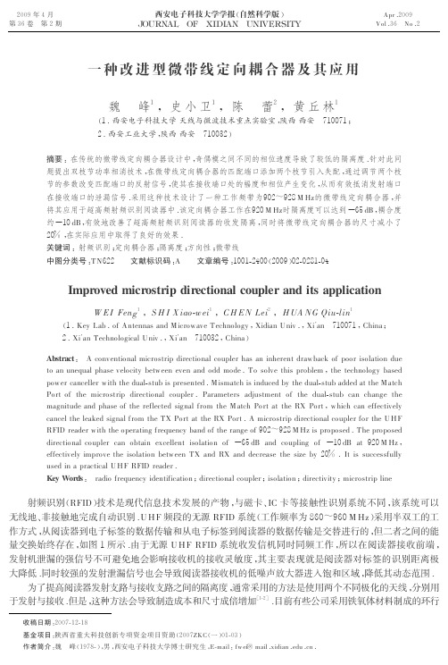
图 4 传统微带线定向耦合器的隔离度和耦合度
图 5 改进的微带线定向耦合器模型
改进的微带线定向耦合器以传统定向耦合器为基础 ,但是在空余端口(端口 4 )引入两个分布元件 :短路
枝节和开路 枝 节 ,如 图 5 所 示 .经 过 优 化 ,各 部 分 尺 寸 为 : L = 46 mm ,W = 2畅 1 mm ,S = 0畅 25 mm ,Lp = 14 mm ;开路枝节位置 Ls = 8畅 5 mm ,开路枝节宽1畅 5 mm ,长 LO = 2畅 6 mm ;短路枝节宽0畅 5 mm ,长30 mm .为了 便于比较 ,同时也仿真了相同尺寸下文献 [6 ]建议的定向耦合器 (经过优化) .两种微带线定向耦合器的仿真比较结果如图 6 所示 .
中端口 4 存在如下关系 :
a4 = Γ b4 .
(2 )
将式(2)代入式(1) ,改进的定向耦合器的 S 参数可表示为一
个3 × 3 阶的矩阵 ,即
b1
C2 Γ T + CΓ I 1 + CΓ T a1
b2 = T + CΓ I
I2 Γ C + T Γ I a2 . (3)
b3
1 + CΓ T C + TΓ I
(1 .西安电子科技大学 天线与微波技术重点实验室 ,陕西 西安 710071 ; 2 .西安工业大学 ,陕西 西安 710032)
定向耦合器基础知识

• 这样可以用一耦合系数来表示小孔的耦合强度。
副波导中的耦合波
A3Cejl Cejl 2Cejl
A4CCej2l 2Ccolse jl
• 端口①输入波行进至小孔a处,耦合至副波导中的 波以 表示向端口③传输的部分,以 表示向端口④ 传输的部分, 为耦合系数。输入波行进至小孔b处 依然向副波导耦合,分为向端口③的 和向端口④ 的 两部分。假定输入波经过小孔a、b后幅值不变 (弱耦合)。
多孔定向耦合器设计
• 多孔耦合定向耦合器,可作成耦合小孔孔径相同 孔距相等,也可作成孔径不同孔距相等。孔径不 同则耦合系数不同,可使它们比例于二项式展开 式中的系数,或比例于切比雪夫多项式等。这种 以元件要素拟合确知函数(曲线)的方法,在电 子信息技术中屡有运用,如多阶梯阻抗变换器、 滤波器设计中寻求所需要的频率特性,天线陈列 设计中为获得所希望的方向性等,读者可根据需 要参阅相关专著。
四 波导窄壁双孔耦合定向耦合器
• 波导窄壁双孔定向耦合器是最简单的波导 定向耦合器,
• 主、副波导通过其公共窄壁上两个相距 l=(2n+1)λ/4 的小孔实现耦合。
1工作原理简析
A
l
B
④ c
c
c
c ③
①
②
A
B
输入波行进至耦合孔a、b时,电磁能通 过小孔耦合至副波导。
小孔耦合
• 电磁能通过小孔耦合、激励的问题,要用小孔 绕射理论来分析,这是微波经典理论中的重要 内容之一,严格求解存在数学上的困难。
S13
2 隔离度
Agilent 796D 797D 798C 方向耦合器操作说明书
ErrataTitle & Document Type: 796D/797D/798C Directional Couplers Operating Note Manual Part Number: 00796-90009Revision Date: November 1977About this ManualWe’ve added this manual to the Agilent website in an effort to help you support your product. This manual provides the best information we could find. It may be incompleteor contain dated information, and the scan quality may not be ideal. If we find a bettercopy in the future, we will add it to the Agilent website.HP References in this ManualThis manual may contain references to HP or Hewlett-Packard. Please note that Hewlett- Packard's former test and measurement, life sciences, and chemical analysisbusinesses are now part of Agilent Technologies. The HP XXXX referred to in this document is now the Agilent XXXX. For example, model number HP8648A is now model number Agilent 8648A. We have made no changes to this manual copy.Support for Your ProductAgilent no longer sells or supports this product. You will find any other availableproduct information on the Agilent Test & Measurement website:Search for the model number of this product, and the resulting product page will guideyou to any available information. Our service centers may be able to perform calibrationif no repair parts are needed, but no other support from Agilent is available.。
实验报告模版9(定向耦合器)
华南理工大学实验报告课程名称射频电路与天线实验电子与信息学院信息工程专业 3 班姓名学号实验名称定向耦合器实验日期指导教师一.实验目的(1)了解定向耦合器的原理及基本测量方法(2)实际测量实验模块,学会用频谱分析仪器测量定性啊耦合器的参数二.实验内容测量耦合器的耦合度、方向性等参数三.实验步骤(1)把AT5011设置为最大衰减量(40dB衰减器全部按下)和最宽扫频范围(1000MHz)。
(2)本实验提供的定线耦合器模块为反定向耦合器,1端口为输入端口,3端口为耦合端口,4端口为隔离端口。
隔离端口P4在内部接一匹配负载,将此端口的能量吸收。
因此本模块只有三个外端口。
首先将频谱分析仪的输入端和输出端用电缆连接,记录直通时跟踪源输出的功率幅度P1。
必要时调节衰减量大小。
但测量过程中不能改变跟踪发生器的输出。
(3)按照图9-5连接实验模块。
P3端口接匹配负载,测量定向耦合器的主线幅度P2。
定向耦合器的插入损耗为:L=P1(dB)-P2(dB)图9-5 测量10dB定向耦合器的主线幅度P2(4)按图9-6连接实验模块。
测量定向耦合器的耦合端输出幅度P3,定向耦合器的耦合度为C=P1(dB)-P3(dB)图9-6 测量10dB定性啊耦合器的耦合端输出幅度P3(5)按图9-7将定向耦合器倒接,这是由P2作为输入端口,P3则变为隔离端口,测量幅度为P4,定向耦合器的隔离度为I=P1-P4,方向性为D=P3-P4。
四.实验数据记录将实验结果录入下表,写出耦合度、隔离度、方向性等参数的计算公式,并计算出最终结果。
计算公式:表9-1五.实验总结。
定向耦合器ppt课件
④
③
图 6-6平行线型耦合器
i1 1
Cm
ic 4
ic 3
4
iL
2
3
图6-7 耦合线方向性的解释
29
同时由于i1的交变磁场的作用,在线4—3 上感应有电流iL。 根据电磁感应定律,感应电流iL的方向与i1 的方向相反, 所以能量从1口输入, 耦合口就是 4口。而在3口因为电耦合电流的ic3与磁耦合电 流iL的相位相反而叠加抵消,故3口是隔离口。
j1
jБайду номын сангаас
/
20
j1
1 j
j
1
e
A A
BC BC
D D
0
2
1
Te A B C D
(1 j) 2
19
对于奇模,
AB
CD
o
4
图 6-5分支线耦合器
13
如果分支线耦合器的各个端口接匹配负载, 信号从1口输入,4口没有输出,为隔离端,2口和3 口的相位差为90°,功率大小由主线和支线的阻 抗决定。
6.3.2 分支线型定向耦合器设计
设计步骤: 步骤一: 确定耦合系数C(dB)、 各端口的 特性阻抗Z0(Ω)、中心频率fc、基板参数 14
(C
Z0e Z0o Z0e Z0o
S14 )
步骤三: 依据基板参数(εr, h),利 用软件ADS计算微带耦合线的宽度及间距(W, S)和四分之一波长的长度(P)。 步骤四: 利用模拟软件检验,再微调。
32
6.4.3 平行耦合线耦合器设计实例
设计一个工作频率为750 MHz的10dB平
ADS设计定向耦合器
<<ADS>>课程设计——分支线耦合器目录1概述 (1)1.1 微波技术产生的背景及发展趋势 (1)1.2 微波电路仿真软件ADS简介 (2)1.3定向耦合概念及分类 (3)1.3.1概念 (3)1.3.2分类 (4)1.3.3 主要技术指标 (6)2工作原理 (7)2.1 传输线理论 (7)2.2 输入阻抗 (8)2.3 特性及测量 (9)2.3.1网络特性 (9)2.3.2测量方法(定向耦合器的特性参量) (10)2.4 定向耦合器的用途 (11)3.微带分支电路的分析与设计 (12)3.1 分支线耦合器 (12)3.2 分支线耦合器的奇偶模分析 (13)4设计过程 (17)4.1 建立工程 (17)4.2 原理图的设计 (18)4.3微带线参数的设置 (19)4.4 VAR控件的设置 (20)4.5 S参数仿真设计 (20)4.6 参数的优化 (22)4.7分支线耦合器版图的生成 (23)5.总结与展望 (25)1概述1.1 微波技术产生的背景及发展趋势微波技术是无线电电子学的一个重要分支,已成为现代通信、雷达、导航和遥感等领域最为敏感的课题之一,发展至今已经有比较久的历史了,无论在理论上还是在实践上,微波科学技术逐渐成熟,并拥有很多的从业人员。
微波波段的电磁波能穿透电离层,因而卫星通信与卫星电视广播、宇宙通信及射电天文学的研究等均需利用微波来实现,在通信、雷达、导航、遥感、天气、气象、工业、农业、医疗以及科学研究等方面得到越来越广泛的应用,成为了无线电电子学的一个重要的分支趋向。
随着通信技术的迅速发展,为了便于携带和移动,无线电设备的小型化是未来的发展趋势,而移动通信所使用频段处于微波范围,因此实现微波电路的更高频率化, 小型化,固体化,不仅在实用方面,而且在学术方面均有重要的研究价值。
定向耦合器通常有两种实现方式: Lange耦合器和带线耦合器。
Lange耦合器具有结构紧凑,便于集成的优点,但一般使用陶瓷基板, 电路制作要求较高,加工工艺和成本限制了它的应用。
- 1、下载文档前请自行甄别文档内容的完整性,平台不提供额外的编辑、内容补充、找答案等附加服务。
- 2、"仅部分预览"的文档,不可在线预览部分如存在完整性等问题,可反馈申请退款(可完整预览的文档不适用该条件!)。
- 3、如文档侵犯您的权益,请联系客服反馈,我们会尽快为您处理(人工客服工作时间:9:00-18:30)。
Agilent 778DDual Directional Coupler100 to 2000 MHzData SheetFeatures• Multi-octave frequency range: 100 to 2000 MHz• High directivity: 36 dB to 1 GHz, 32 dB to 2 GHz• Reflection coefficient measurement: Over 4 octaves with 1 couplerBroadband 20 dB Dual Directional CouplerThis dual directional 20 dB coupler has a frequency range extending over 4 octaves from 100 MHz to 2 GHz. The multi-octave capability makes measurements easier–setup and calibration time are reduced, since normally several couplers are required over this frequency band. The coupling factor increases about 6 dB per octave below 100 MHz; thus, usefulness below this frequency is restricted only by the amount of signal source power and/or the sensitivity of the RF detector con-nected to the coupler. Figure 1 shows typical coupling and directivity characteristics of the 778D.0.1 to 1 GHz± (0.015 + 0.02 |GL | + 0.05 |GL|2)± (0.015 + 0.05 |GL|2)1 to2 GHz± (0.025 + 0.02 |GL | + 0.05 |GL|2)± (0.025 + 0.05 |GL|2)Maximum phase error = ±sin-1 (∆G L/G L)|GL |= reflection coefficient of unknownThe 778D is ideal for measuring the reflection and transmission characteristics of a device from 100 MHz to 2000 MHz. Figure 2 shows a test configurationin which a 778D dual directional coupler is used to separate and isolate theincident, reflected, and transmitted signals in a swept-frequency measurement.These signals are detected and their ratio displayed on a CRT. This coupler is an ideal companion for the Agilent 8755 frequency response test set, a detectionand display system operating from 15 MHz to 18 GHz.The high directivity and close tracking of the auxiliary arms of this couplermake it particularly useful for this type of broadband measurement. The highdirectivity insures accurate measurements by a true separation of the forwardand reflected signals. Close tracking of signal variation from the auxiliary armsgives a flat frequency response that makes display readings easy to interpret.Maximum amplitude errors in a reflection measuring system are shown in thefollowing tableFigure 1. Coupling and directivity characteristics of the 778D coupler.Figure 2. Setup diagram for simultaneous measurements of insertion and return loss.Simultaneous Reflection and Transmission MeasurementsImpedance MeasurementsSystem Monitoring Choice of Output Connectors Error components include a fixed term due to coupler directivity, and severalGL-dependent terms relating to source match and reference setting (detection errors are not included). These errors apply over broad swept-frequency bands. Somewhat improved accuracy can be achieved by simple recalibration at the frequency of interest.The 778D is also well suited for measurements of impedance when used with the Agilent 8405A vector voltmeter. The technique is described in Application Note 77-3, Measurement of Complex Impedance, available at your nearest Agilent sales office. Again, a reflectometry technique is used. With the vector voltmeter, however, both magnitude and phase angle of the reflection coefficient can be measured. This setup is shown in Figure 3.Data can be read from the two meters of the vector voltmeter and transferred directly to a Smith Chart to provide impedance of such devices as antennas or other passive components. In addition, with an appropriate bias supply, active components, such as transistors, can also be quickly measured and character-ized with this setup. The 778D is well-suited for these types of measurements since both the phase and the magnitude variation between the two coupling arms have been closely controlled in the design of the coupler.Because of the high power capability of the dual directional coupler, it canbe permanently installed in coaxial systems to monitor the power traveling in both directions simultaneously. This enables a system to be continually moni-tored to indicate whether the system is in need of adjustment or maintenance due to excessive standing-wave rations on the transmission lines.To achieve its broad frequency coverage, the 778D’s directivity is optimizedfor mainline energy flowing in one direction, Thus, the test device or system should be connected where the 778D is labeled TEST PORT. To accommodate test devices with type-N or APC-71 connectors, a choice of connectors is avail-able on the TEST PORT; see the options outlined under Specifications.The APC-7 precision sexless connector is recommended on the output, since the coupler can be conveniently converted to other types of connectors by use of an adapter, Adapters are available to OSM, TNC, GR900, and others, so that the coupler becomes a versatile device for making measurements on many different types of connector configurations. The Amphenol, APC-7 is a sexless connector with very low SWR. This precision connector makes possible the construction of adapters with the lowest possible SWR.The type-N connectors are stainless steel for long wear and are compatiblewith connectors whose dimensions conform to MIL-C-39012, or MIL-C-71. Figure 3. Setup of impedance measurement of coaxial devices from ~10 to 1000 MHz.Remove all doubtFor more information on repair and calibration services, go to:/find/removealldoubtAgilent Email Updates/find/emailupdatesGet the latest information on theproducts and applications you select.For more information on AgilentTechnologies’ products, applicationsor services, please contact your localAgilent office. The complete list isavailable at:/find/contactusAmericasCanada (877)894-4414Latin America 305 269 7500United States (800) 829-4444Asia PacificAustralia 1 800 629 485China 800 810 0189Hong Kong 800 938 693India 1 800 112 929Japan 0120 (421) 345Korea 080 769 0800Malaysia 1 800 888 848Singapore 1 800 375 8100Taiwan 0800 047 866Thailand 1 800 226 008Europe & Middle EastAustria 01 36027 71571Belgium 32 (0) 2 404 93 40Denmark 45 70 13 15 15Finland 358 (0) 10 855 2100France 0825 010 700**0.125€/minuteGermany 07031 464 6333Ireland 1890 924 204Israel 972-3-9288-504/544Italy 39 02 92 60 8484Netherlands 31 (0) 20 547 2111Spain 34 (91) 631 3300Sweden 0200-88 22 55Switzerland 0800 80 53 53United Kingdom 44 (0) 118 9276201Other European Countries:/find/contactusRevised: July 2, 2009Product specifications and descriptionsin this document subject to changewithout notice.© Agilent Technologies, Inc. 2004, 2009Printed in USA, September 11, 20095952-8133/find/mtaSpecificationsFrequency range100 MHz to 2000 MHz (usable below 100 MHz)Directivity Auxiliary arm 0.1 to 1 GHz 1 to 2 GHzA 36 dB 32 dBB 30 dB 30 dBCoupling factor20 dB nominal ±1 dB cyclic variation with frequency (coupling~23 dB at 100 MHz. 6 dB rolloff per octave below 100 MHz). Tracking Auxiliary outputs typically track within 0.7 dB.Phase tracking typically 4°.SWR Primary line: 1.1; auxiliary arms: 1.1.Insertion loss 0.6 dBMaximum power50 W average; 500 W peak (peak power duration of 10us). Connectors Choice of mainline connectors (see options); auxiliary armshave type-N female connectors, All type-N connectors stain-less steel, compatible with MIL-C-39012 and MIL-C-71. Dimensions16.75 inches long, 4.375 inches high, 1.189 inches wide(425 x 111 x 30 mm).Weight Net, 3.75 lb (1,5 kg). Shipping, 5 lb (2,3 kg). Accessories availableAdapters Part numberAPC-7 to OSM® male 11533AAPC-7 to OSM female 11534AAPC-7 to type-N male 11525AAPC-7 to type-N female 11524A(Adapters from APC-7 to TNC, GR-900, GR-874 as well as the above are available from Amphenol RF Division, Danbury, Conn.)778D (type-N female output, type-N male input connectors)Option 11 (APC-7 output, type-N female input connectors)Option 12 (type-N male output, type-N female input connectors)。