Limited-pool random frequency for DC brush motor low frequency PWM speed control
芯片科技 EFR32FG28 双频子GHz + 2.4GHz BLE SoC 产品说明书

EFR32FG28 Wireless SoC Family Data ShortThe EFR32FG28 SoC is an ideal dual band Sub-GHz + 2.4 GHz BLE SoC solution for “Internet of Things” applications in smart homes, security, lighting, building automation,and metering. This dual band solution combines a high-performance Sub-GHz radio that provides long range capabilities and a 2.4 GHz BLE radio for multiprotocol applications.The single die, multi-core solution, provides industry leading security, low power con-sumption with fast wakeup times, and integrated power amplifiers to enable the next lev-el of secure connectivity for IoT devices. Large memory footprint enables flexible solu-tions for Dynamic Protocol support and the integration of a Matrix Vector Processor em-powers AI/ML implementation for Smart End Nodes.EFR32FG28 applications include:KEY FEATURES•32-bit ARM® Cortex®-M33 core with 78MHz maximum operating frequency •1024 kB of flash and up to 256 kB of RAM •Energy-efficient radio core with low active and sleep currents•Integrated PAs with up to 20 dBm for sub-GHz and 10 dBm for BLE transmit power •Robust peripheral set and up to 49 GPIO •QFN48 and QFN68 package options•Metering•Home and Building Automation and Security •Industrial Automation •Street LightingTimers and Triggers 32-bit busPeripheral Reflex SystemSerial InterfacesI/O PortsAnalog I/FLowest power mode with peripheral operational:USARTEUSARTExternal Interrupts General Purpose I/O Pin ResetPin Wakeup IADCEM4—ShutoffEnergy ManagementBrown-Out DetectorVoltage RegulatorPower-On Reset SecurityClock ManagementHF Crystal OscillatorLF Crystal OscillatorLFRC Oscillator HFRC Oscillator Ultra LF RC OscillatorCore / MemoryARM Cortex M33 processorwith DSP extensions,FPU and TrustZoneETM Debug Interface RAM MemoryLDMA Controller System Real TimeCounter Timer/CounterLow Energy Timer Watchdog Timer Protocol TimerEM3—StopEM2—Deep SleepEM1—SleepEM0—ActiveFast Startup RC OscillatorBack-Up Real Time CounterI CEUSART DC-DC ConverterVDACRadio SubsystemSub-GHz RX/TX Frontend with Integrated +14 or 20 dBm PA 2.4 GHz BLE RX/TX Frontend with Integrated +10 dBm PAFrequency SynthesizerARM Cortex TM M0+ Radio Controller CRCBUFC RAMFRC DEMODAGCIFADCMODSecure Debug AuthenticationCrypto Acceleration Secure EngineTrue Random Number Generator DPACountermeasuresTemperature SensorACMPLCDLESENSE Pulse CounterKeypad ScannerFlash ProgramMemoryAI/ML Hardware Accelerator (MVP)1. Feature ListThe EFR32FG28 highlighted features are listed below.•Low Power Wireless System-on-Chip•High Performance 32-bit 78 MHz ARM Cortex®-M33 withDSP instruction and floating-point unit for efficient signalprocessing•Up to 1024 kB flash program memory•Up to 256 kB RAM data memory•Sub-GHz radio operation with TX power up to +20 dBm• 2.4 GHz BLE radio operation with TX power up to +10 dBm •Matrix Vector Processor for AI/ML acceleration•Low Energy Consumption• 5 mA RX current at 920 MHz (400 kbps 4-FSK)• 4.6 mA RX current at 915 MHz (4.8 kbps O-QPSK)• 6.1 mA RX current at 915 MHz (2 Mbps GFSK)• 4.6 mA RX current at 868 MHz (2.4 kbps GFSK)• 4.6 mA RX current at 868 MHz (38.4 kbps FSK)• 4.1 mA RX current at 433 MHz (100 kbps 2GFSK)• 5.2 mA RX current at 2.4 GHz, 1 Mbps BLE•26.2 mA TX current @ 14 dBm output power at 915 MHz(14 dBm part numbers)•12.2 mA TX current @ 0 dBm output power, 2.4 GHz•22.5 mA TX current @ 10 dBm output power, 2.4 GHz•33 μA/MHz in Active Mode (EM0) at 39.0 MHz• 2.8 μA EM2 DeepSleep current (256 kB RAM retention and RTC running from LFXO)• 1.3 μA EM2 DeepSleep current (16 kB RAM retention andRTC running from LFRCO)•Preamble Sense Mode (PSM) low duty-cycle listen•High Receiver Performance•-98.6 dBm sensitivity @ 400 kbps 920 MHz 4-GFSK•****************************************•-96.9 dBm sensitivity @ 2 Mbps 915 MHz GFSK•**************************************•**************************************•-110.7 dBm sensitivity @ 100 kbps 433 MHz 2GFSK •Supported Modulation Format•2/4 (G)FSK with fully configurable shaping•OQPSK DSSS•(G)MSK•OOK•Protocol Support•Proprietary•CONNECT•Amazon Sidewalk•WM-BUS•Wi-SUN•Bluetooth Low Energy •Wide selection of MCU peripherals•Analog to Digital Converter (ADC)•12-bit @ 1 Msps•***************• 2 × Analog Comparator (ACMP)•2-Channel Digital to Analog Converter (VDAC)•Low-Energy Sensor Interface (LESENSE)•Up to 49 General Purpose I/O pins with output state reten-tion and asynchronous interrupts•8 Channel DMA Controller•12 Channel Peripheral Reflex System (PRS)• 4 × 16-bit Timer/Counter with 3 Compare/Capture/PWMchannels• 1 × 32-bit Timer/Counter with 3 Compare/Capture/PWMchannels•32-bit Real Time Counter•24-bit Low Energy Timer for waveform generation•16-bit Pulse Counter with asynchronous operation (PCNT)• 2 × Watchdog Timer• 3 × Enhanced Universal Synchronous/Asynchronous Re-ceiver/Transmitter (EUSART)• 1 × Universal Synchronous/Asynchronous Receiver/Trans-mitter (UART/SPI/SmartCard (ISO 7816)/IrDA/I2S)• 2 × I2C interface with SMBus support•Integrated Low-Energy LCD Controller supporting up to 192 segments•Keypad scanner supporting up to 6×8 matrix (KEYSCAN)•Die temperature sensor with ±2 °C typical accuracy acrosstemperature range•Secure Vault•Hardware Cryptographic Acceleration for AES128/192/256,ChaCha20-Poly1305, SHA-1, SHA-2/256/384/512, ECDSA+ECDH(P-192, P-256, P-384, P-521), Ed25519 andCurve25519, J-PAKE, PBKDF2•True Random Number Generator (TRNG)•ARM® TrustZone®•Secure Boot (Root of Trust Secure Loader)•Secure Debug Unlock•DPA Countermeasures•Secure Key Management with PUF•Anti-Tamper•Secure Attestation•Wide Operating Range• 1.71 V to 3.8 V single power supply•-40 °C to +125 °C•Packages•QFN68 8 mm × 8 mm × 0.85 mm•QFN48 6 mm × 6 mm × 0.85 mmFeature List2. Ordering InformationTable 2.1. Ordering InformationProduct FamilySecurityFeaturesMemoryTemperature GradeSizePackagePinsRevisionTape & ReelEFR32FG28A 322F 1024I M 68A R-Figure 2.1. Ordering Code KeySilicon Laboratories Inc.400 West Cesar Chavez Austin, TX 78701USAIoT Portfolio/IoTSW/HW/simplicityQuality /qualitySupport & Community/communityDisclaimerSilicon Labs intends to provide customers with the latest, accurate, and in-depth documentation of all peripherals and modules available for system and software imple-menters using or intending to use the Silicon Labs products. Characterization data, available modules and peripherals, memory sizes and memory addresses refer to each specific device, and “Typical” parameters provided can and do vary in different applications. Application examples described herein are for illustrative purposes only. Silicon Labs reserves the right to make changes without further notice to the product information, specifications, and descriptions herein, and does not give warranties as to the accuracy or completeness of the included information. Without prior notification, Silicon Labs may update product firmware during the manufacturing process for security or reliability reasons. Such changes will not alter the specifications or the performance of the product. Silicon Labs shall have no liability for the consequences of use of the infor -mation supplied in this document. This document does not imply or expressly grant any license to design or fabricate any integrated circuits. The products are not designed or authorized to be used within any FDA Class III devices, applications for which FDA premarket approval is required or Life Support Systems without the specific written consent of Silicon Labs. A “Life Support System” is any product or system intended to support or sustain life and/or health, which, if it fails, can be reasonably expected to result in significant personal injury or death. Silicon Labs products are not designed or authorized for military applications. Silicon Labs products shall under no circumstances be used in weapons of mass destruction including (but not limited to) nuclear, biological or chemical weapons, or missiles capable of delivering such weapons. Silicon Labs disclaims all express and implied warranties and shall not be responsible or liable for any injuries or damages related to use of a Silicon Labs product in such unauthorized applications. Note: This content may contain offensive terminology that is now obsolete. Silicon Labs is replacing these terms with inclusive language wherever possible. For more information, visit /about-us/inclusive-lexicon-projectTrademark InformationSilicon Laboratories Inc.®, Silicon Laboratories ®, Silicon Labs ®, SiLabs ® and the Silicon Labs logo ®, Bluegiga ®, Bluegiga Logo ®, EFM ®, EFM32®, EFR, Ember ®, Energy Micro, Energy Micro logo and combinations thereof, “the world’s most energy friendly microcontrollers”, Redpine Signals ®, WiSeConnect , n-Link, ThreadArch ®, EZLink ®, EZRadio ®, EZRadioPRO ®, Gecko ®, Gecko OS, Gecko OS Studio, Precision32®, Simplicity Studio ®, Telegesis, the Telegesis Logo ®, USBXpress ® , Zentri, the Zentri logo and Zentri DMS, Z-Wave ®, and others are trademarks or registered trademarks of Silicon Labs. ARM, CORTEX, Cortex-M3 and THUMB are trademarks or registered trademarks of ARM Holdings. Keil is a registered trademark of ARM Limited. Wi-Fi is a registered trademark of the Wi-Fi Alliance. All other products or brand names mentioned herein are trademarks of their respective holders.。
Eaton DC1-12015NB-A66N 可变频率驱动器说明书
Brake chopper 7-digital display assembly
FS3
with SmartWire-DT module DX-NET-SWD2
Specification for general requirements: IEC/EN 61800-2 EMC requirements: IEC/EN 61800-3 Safety requirements: IEC/EN 61800-5-1
In
Heat dissipation per pole, current-dependent
Pvid
Equipment heat dissipation, current-dependent
Pvid
Static heat dissipation, non-current-dependent
Pvs
Heat dissipation capacity
Degree of Protection Protection against direct contact
This item will continue to be available for a limited time only and is being replaced by the following item: 185801, DC1-12015NB-A66CE1
max. 30 % MN adjustable to 100 %
Max. 100% of rated operational current Ie with external braking resistor
Ω
25
V
390 V DC
V
10 V DC (max. 10 mA)
L6207PD 电机驱动芯片
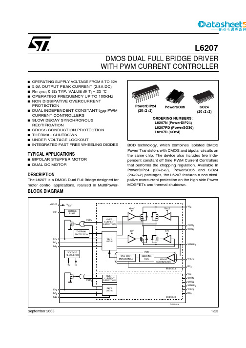
1/23L6207September 2003 s OPERATING SUPPLY VOLTAGE FROM 8 TO 52V s 5.6A OUTPUT PEAK CURRENT (2.8A DC)s R DS(ON) 0.3Ω TYP. VALUE @ T j = 25 °C s OPERATING FREQUENCY UP TO 100KHz s NON DISSIPATIVE OVERCURRENT PROTECTIONs DUAL INDEPENDENT CONSTANT t OFF PWM CURRENT CONTROLLERSs SLOW DECAY SYNCHRONOUS RECTIFICATIONs CROSS CONDUCTION PROTECTION s THERMAL SHUTDOWNs UNDER VOLTAGE LOCKOUTsINTEGRATED FAST FREE WHEELING DIODESTYPICAL APPLICATIONSs BIPOLAR STEPPER MOTOR s DUAL DC MOTORDESCRIPTIONThe L6207 is a DMOS Dual Full Bridge designed for motor control applications, realized in MultiPower-BCD technology, which combines isolated DMOS Power Transistors with CMOS and bipolar circuits on the same chip. The device also includes two inde-pendent constant off time PWM Current Controllers that performs the chopping regulation. Available in PowerDIP24 (20+2+2), PowerSO36 and SO24(20+2+2) packages, the L6207 features a non-dissi-pative overcurrent protection on the high side Power MOSFETs and thermal shutdown.BLOCK DIAGRAMDMOS DUAL FULL BRIDGE DRIVER WITH PWM CURRENT CONTROLLERL62072/23ABSOLUTE MAXIMUM RATINGSRECOMMENDED OPERATING CONDITIONSSymbol ParameterTest conditionsValue Unit V S Supply VoltageV SA = V SB = VS60V V ODDifferential Voltage between VS A , OUT1A , OUT2A , SENSE A and VS B , OUT1B , OUT2B , SENSE B V SA = V SB = V S = 60V;V SENSEA = V SENSEB = GND 60VV BOOT Bootstrap Peak Voltage V SA = V SB = V SV S + 10V V IN ,V EN Input and Enable Voltage Range -0.3 to +7V V REFA , V REFBVoltage Range at pins V REFA and V REFB-0.3 to +7V V RCA, V RCB Voltage Range at pins RC A andRC B -0.3 to +7V V SENSEA, V SENSEB Voltage Range at pins SENSE A and SENSE B-1 to +4V I S(peak)Pulsed Supply Current (for each V S pin), internally limited by the overcurrent protection V SA = V SB = V S ;t PULSE < 1ms 7.1AI S RMS Supply Current (for each V S pin)V SA = V SB = V S2.8A T stg , T OPStorage and Operating Temperature Range-40 to 150°CSymbol ParameterTest ConditionsMIN MAX Unit V S Supply VoltageV SA = V SB = V S852V V ODDifferential Voltage Between VS A , OUT1A , OUT2A , SENSE A and VS B , OUT1B , OUT2B , SENSE B V SA = V SB = V S ;V SENSEA = V SENSEB 52VV REFA , V REFB Voltage Range at pins V REFA and V REFB-0.15V V SENSEA, V SENSEB Voltage Range at pins SENSE A and SENSE B (pulsed t W < t rr )(DC)-6-161V V I OUT RMS Output Current2.8A T j Operating Junction Temperature -25+125°C f swSwitching Frequency100KHz3/23L6207THERMAL DATA(5)The slug is internally connected to pins 1,18,19 and 36 (GND pins).Symbol DescriptionPowerDIP24SO24PowerSO36Unit R th-j-pins Maximum Thermal Resistance Junction-Pins 1814-°C/W R th-j-case Maximum Thermal Resistance Junction-Case --1°C/W R th-j-amb1Maximum Thermal Resistance Junction-Ambient 1(1)Mounted on a multi-layer FR4 PCB with a dissipating copper surface on the bottom side of 6cm 2 (with a thickness of 35µm).4351-°C/W R th-j-amb1Maximum Thermal Resistance Junction-Ambient 2(2)Mounted on a multi-layer FR4 PCB with a dissipating copper surface on the top side of 6cm 2 (with a thickness of 35µm).--35°C/W R th-j-amb1Maximum Thermal Resistance Junction-Ambient 3(3)Mounted on a multi-layer FR4 PCB with a dissipating copper surface on the top side of 6cm 2 (with a thickness of 35µm), 16 via holes and a ground layer.--15°C/W R th-j-amb2Maximum Thermal Resistance Junction-Ambient 4(4)Mounted on a multi-layer FR4 PCB without any heat sinking surface on the board.587762°C/WL62074/23PIN DESCRIPTIONPACKAGENameTypeFunctionSO24/PowerDIP24PowerSO36PIN #PIN #110IN1A Logic input Bridge A Logic Input 1.211IN2A Logic input Bridge A Logic Input 2.312SENSE A Power SupplyBridge A Source Pin. This pin must be connected to Power Ground through a sensing power resistor.413RC ARC PinRC Network Pin. A parallel RC network connectedbetween this pin and ground sets the Current Controller OFF-Time of the Bridge A.515OUT1A Power OutputBridge A Output 1.6, 7,18, 191, 18,19, 36GNDGNDSignal Ground terminals. In Power DIP and SO packages, these pins are also used for heat dissipation toward the PCB.822OUT1B Power Output Bridge B Output 1.924RC BRC PinRC Network Pin. A parallel RC network connectedbetween this pin and ground sets the Current Controller OFF-Time of the Bridge B.1025SENSE B Power Supply Bridge B Source Pin. This pin must be connected to Power Ground through a sensing power resistor.1126IN1B Logic Input Bridge B Input 11227IN2B Logic Input Bridge B Input 21328VREF B Analog Input Bridge B Current Controller Reference Voltage. Do not leave this pin open or connect to GND.1429EN BLogic Input (6)Bridge B Enable. LOW logic level switches OFF all Power MOSFETs of Bridge B. This pin is also connected to the collector of the Overcurrent and Thermal Protection transistor to implement over current protection.If not used, it has to be connected to +5V through a resistor.1530VBOOT Supply Voltage Bootstrap Voltage needed for driving the upper Power MOSFETs of both Bridge A and Bridge B.1632OUT2B Power OutputBridge B Output 2.1733VS B Power Supply Bridge B Power Supply Voltage. It must be connected tothe supply voltage together with pin VS A .204VS A Power Supply Bridge A Power Supply Voltage. It must be connected to the supply voltage together with pin VS B .215OUT2A Power OutputBridge A Output 2.227VCPOutputCharge Pump Oscillator Output.5/23L6207(6)Also connected at the output drain of the Over current and Thermal protection MOSFET. Therefore, it has to be driven putting in series a resistor with a value in the range of 2.2K Ω - 180K Ω, recommended 100K Ω.238EN ALogic Input (6)Bridge A Enable. LOW logic level switches OFF all Power MOSFETs of Bridge A. This pin is also connected to the collector of the Overcurrent and Thermal Protection transistor to implement over current protection.If not used, it has to be connected to +5V through a resistor.249VREF A Analog InputBridge A Current Controller Reference Voltage. Do not leave this pin open or connect to GND.ELECTRICAL CHARACTERISTICS(T amb = 25 °C, V s = 48V, unless otherwise specified)Symbol Parameter Test ConditionsMin Typ Max Unit V Sth(ON)Turn-on Threshold6.677.4V V Sth(OFF)Turn-off Threshold5.66 6.4V I S Quiescent Supply Current All Bridges OFF;T j = -25°C to 125°C (7)510mA T j(OFF)Thermal Shutdown Temperature165°COutput DMOS Transistors R DS(ON)High-Side Switch ON Resistance T j = 25 °C0.340.4ΩT j =125 °C (7)0.530.59ΩLow-Side Switch ON ResistanceT j = 25 °C 0.280.34ΩT j =125 °C (7)0.470.53ΩI DSSLeakage CurrentEN = Low; OUT = V S 2mA EN = Low; OUT = GND-0.15mASource Drain Diodes V SD Forward ON Voltage I SD = 2.8A, EN = LOW 1.15 1.3V t rr Reverse Recovery Time I f = 2.8A300ns t frForward Recovery Time200nsLogic Input V IL Low level logic input voltage -0.30.8V V IH High level logic input voltage 27V I IL Low Level Logic Input Current GND Logic Input Voltage -10µA I IH High Level Logic Input Current 7V Logic Input Voltage10µA V th(ON)Turn-on Input Threshold 1.8 2.0V V th(OFF)Turn-off Input Threshold 0.8 1.3V V th(HYS)Input Threshold Hysteresis0.250.5VPIN DESCRIPTION (continued)L62076/23(8)See Fig. 1.(9)Measured applying a voltage of 1V to pin SENSE and a voltage drop from 2V to 0V to pin VREF.(10)See Fig. 2.Switching Characteristics t D(on)EN Enable to out turn ON delay time (8)I LOAD =2.8A, Resistive Load 100250400ns t D(on)IN Input to out turn ON delay time I LOAD =2.8A, Resistive Load(dead time included) 1.6µs t RISE Output rise time (8)I LOAD =2.8A, Resistive Load40250ns t D(off)EN Enable to out turn OFF delay time (8)I LOAD =2.8A, Resistive Load 300550800ns t D(off)IN Input to out turn OFF delay time I LOAD =2.8A, Resistive Load 600ns t FALL Output Fall Time (8)I LOAD =2.8A, Resistive Load40250ns t dt Dead Time Protection 0.51µs f CPCharge pump frequency-25°C<T j <125°C0.61MHzPWM Comparator and Monostable I RCA, I RCB Source Current at pins RC A andRC B V RCA = V RCB = 2.5V 3.55.5mA V offset Offset Voltage on Sense ComparatorV REFA, V REFB = 0.5V±5mV t PROP Turn OFF Propagation Delay (9)500ns t BLANK Internal Blanking Time on SENSE pins 1µs t ON(MIN)Minimum On Time 1.52µs t OFFPWM Recirculation TimeR OFF = 20K Ω; C OFF = 1nF 13µs R OFF = 100K Ω; C OFF = 1nF61µs I BIASInput Bias Current at pins VREF A and VREF B10µAOver Current Protection ELECTRICAL CHARACTERISTICS (continued)(T amb = 25 °C, V s = 48V, unless otherwise specified)SymbolParameter Test ConditionsMinTypMax UnitL62077/23L62078/23CIRCUIT DESCRIPTIONPOWER STAGES and CHARGE PUMPThe L6207 integrates two independent Power MOS Full Bridges. Each Power MOS has an Rdson =0.3ohm (typical value @ 25°C), with intrinsic fast freewheeling diode. Cross conduction protection is achieved using a dead time (td = 1µs typical) be-tween the switch off and switch on of two Power MOS in one leg of a bridge.Using N Channel Power MOS for the upper transis-tors in the bridge requires a gate drive voltage above the power supply voltage. The Bootstrapped (VBOOT) supply is obtained through an internal Os-cillator and few external components to realize a charge pump circuit as shown in Figure 3. The oscil-lator output (VCP) is a square wave at 600kHz (typi-cal) with 10V amplitude. Recommended values/part numbers for the charge pump circuit are shown in Table1.Table 1. Charge Pump External ComponentsValuesLOGIC INPUTSPins IN1A , IN2B , IN1B and IN2B are TTL/CMOS and uC compatible logic inputs. The internal structure is shown in Fig. 4. Typical value for turn-on and turn-off thresholds are respectively Vthon = 1.8V and Vthoff = 1.3V.Pins EN A and EN B have identical input structure with the exception that the drains of the Overcurrent andthermal protection MOSFETs (one for the Bridge A and one for the Bridge B) are also connected to these pins. Due to these connections some care needs to be taken in driving these pins. The EN A and EN B in-puts may be driven in one of two configurations as shown in figures 5 or 6. If driven by an open drain (collector) structure, a pull-up resistor R EN and a ca-pacitor C EN are connected as shown in Fig. 5. If the driver is a standard Push-Pull structure the resistor R EN and the capacitor C EN are connected as shown in Fig. 6. The resistor R EN should be chosen in the range from 2.2k Ω to 180K Ω. Recommended values for R EN and C EN are respectively 100K Ω and 5.6nF.More information on selecting the values is found in the Overcurrent Protection section.Figure 5. EN A and EN B Pins Open CollectorC BOOT 220nF C P 10nF R P 100ΩD11N4148D21N41489/23L6207TRUTH TABLEX = Don't care High Z = High Impedance OutputGND (Vs)= GND during Ton, Vs during Toff(*) Valid only in case of load connected between OUT1 and OUT2PWM CURRENT CONTROLThe L6207 includes a constant off time PWM current controller for each of the two bridges. The current control circuit senses the bridge current by sensing the voltage drop across an external sense resistor connected be-tween the source of the two lower power MOS transistors and ground, as shown in Figure 7. As the current in the load builds up the voltage across the sense resistor increases proportionally. When the voltage drop across the sense resistor becomes greater than the voltage at the reference input (VREF A or VREF B ) the sense com-parator triggers the monostable switching the low-side MOS off. The low-side MOS remain off for the time set by the monostable and the motor current recirculates in the upper path. When the monostable times out the bridge will again turn on. Since the internal dead time, used to prevent cross conduction in the bridge, delays the turn on of the power MOS, the effective off time is the sum of the monostable time plus the dead time.Figure 8 shows the typical operating waveforms of the output current, the voltage drop across the sensing re-sistor, the RC pin voltage and the status of the bridge. Immediately after the low-side Power MOS turns on, a high peak current flows through the sensing resistor due to the reverse recovery of the freewheeling diodes. The L6207 provides a 1µs Blanking Time t BLANK that inhibits the comparator output so that this current spike cannot prematurely re-trigger the monostable.INPUTSOUTPUTSDescription (*)EN IN1IN2OUT1OUT2L X X High Z High Z DisableH L L GND GND Brake Mode (Lower Path)H H L Vs GND (Vs)Forward H L H GND (Vs)Vs ReverseHHHVsVsBrake Mode (Upper Path)L620710/23Figure 9 shows the magnitude of the Off Time t OFF versus C OFF and R OFF values. It can be approximately cal-culated from the equations:t RCFALL = 0.6 · R OFF · C OFFt OFF = t RCFALL + t DT = 0.6 · R OFF · C OFF + t DTwhere R OFF and C OFF are the external component values and t DT is the internally generated Dead Time with:20K Ω ≤ R OFF ≤ 100K Ω0.47nF ≤ C OFF ≤ 100nF t DT = 1µs (typical value)Therefore:t OFF(MIN) = 6.6µs t OFF(MAX) = 6msThese values allow a sufficient range of t OFF to implement the drive circuit for most motors.The capacitor value chosen for C OFF also affects the Rise Time t RCRISE of the voltage at the pin RCOFF. The Rise Time t RCRISE will only be an issue if the capacitor is not completely charged before the next time the monostable is triggered. Therefore, the on time t ON , which depends by motors and supply parameters, has to11/23be bigger than t RCRISE for allowing a good current regulation by the PWM stage. Furthermore, the on time t ON can not be smaller than the minimum on time t ON(MIN).t RCRISE = 600 · C OFFFigure 10 shows the lower limit for the on time t ON for having a good PWM current regulation capacity. It has to be said that t ON is always bigger than t ON(MIN) because the device imposes this condition, but it can be smaller than t RCRISE - t DT . In this last case the device continues to work but the off time t OFF is not more constant.So, small C OFF value gives more flexibility for the applications (allows smaller on time and, therefore, higher switching frequency), but, the smaller is the value for C OFF , the more influential will be the noises on the circuit performance.t ON t ON MIN ()> 1.5µs (typ. value)=t ON t RCRISE t DT–>SLOW DECAY MODEFigure 11 shows the operation of the bridge in the Slow Decay mode. At the start of the off time, the lower power MOS is switched off and the current recirculates around the upper half of the bridge. Since the voltage across the coil is low, the current decays slowly. After the dead time the upper power MOS is operated in the synchro-nous rectification mode. When the monostable times out, the lower power MOS is turned on again after some delay set by the dead time to prevent cross conduction.12/23NON-DISSIPATIVE OVERCURRENT PROTECTIONThe L6207 integrates an Overcurrent Detection Circuit (OCD). This circuit provides protection against a short circuit to ground or between two phases of the bridge. With this internal over current detection, the external cur-rent sense resistor normally used and its associated power dissipation are eliminated. Figure 12 shows a sim-plified schematic of the overcurrent detection circuit.To implement the over current detection, a sensing element that delivers a small but precise fraction of the out-put current is implemented with each high side power MOS. Since this current is a small fraction of the output current there is very little additional power dissipation. This current is compared with an internal reference cur-rent I REF. When the output current in one bridge reaches the detection threshold (typically 5.6A) the relative OCD comparator signals a fault condition. When a fault condition is detected, the EN pin is pulled below the turn off threshold (1.3V typical) by an internal open drain MOS with a pull down capability of 4mA. By using an ex-ternal R-C on the EN pin, the off time before recovering normal operation can be easily programmed by means of the accurate thresholds of the logic inputs.Figure 13 shows the Overcurrent Detection operation. The Disable Time t DISABLE before recovering normal oper-ation can be easily programmed by means of the accurate thresholds of the logic inputs. It is affected whether by C EN and R EN values and its magnitude is reported in Figure 14. The Delay Time t DELAY before turning off the bridge when an overcurrent has been detected depends only by C EN value. Its magnitude is reported in Figure 15.C EN is also used for providing immunity to pin EN against fast transient noises. Therefore the value of C EN should be chosen as big as possible according to the maximum tolerable Delay Time and the R EN value should be chosen according to the desired Disable Time.The resistor R EN should be chosen in the range from 2.2KΩ to 180KΩ. Recommended values for R EN and C EN are respectively 100KΩ and 5.6nF that allow obtaining 200µs Disable Time.13/2314/23THERMAL PROTECTIONIn addition to the Ovecurrent Protection, the L6207 integrates a Thermal Protection for preventing the device destruction in case of junction over temperature. It works sensing the die temperature by means of a sensible element integrated in the die. The device switch-off when the junction temperature reaches 165°C (typ. value) with 15°C hysteresis (typ. value).15/23APPLICATION INFORMATIONA typical application using L6207 is shown in Fig. 16. Typical component values for the application are shown in Table 3. A high quality ceramic capacitor in the range of 100 to 200 nF should be placed between the power pins (VS A and VS B) and ground near the L6207 to improve the high frequency filtering on the power supply and reduce high frequency transients generated by the switching. The capacitors connected from the EN A and ENB inputs to ground set the shut down time for the BrgidgeA and BridgeB respectively when an over current is de-tected (see Overcurrent Protection). The two current sensing inputs (SENSE A and SENSE B) should be connect-ed to the sensing resistors with a trace length as short as possible in the layout. The sense resistors should be non-inductive resistors to minimize the di/dt transients across the resistor. To increase noise immunity, unused logic pins (except EN A and EN B) are best connected to 5V (High Logic Level) or GND (Low Logic Level) (see pin description). It is recommended to keep Power Ground and Signal Ground separated on PCB.Table 2. Component Values for Typical ApplicationC1100uF D11N4148C2100nF D21N4148C A1nF R A39KΩC B1nF R B39KΩC BOOT220nF R ENA100KΩC P10nF R ENB100KΩC ENA 5.6nF R P100ΩC ENB 5.6nF R SENSEA0.3ΩC REFA68nF R SENSEB0.3ΩC REFB68nF16/23OUTPUT CURRENT CAPABILITY AND IC POWER DISSIPATIONIn Fig. 17 and Fig. 18 are shown the approximate relation between the output current and the IC power dissipa-tion using PWM current control driving two loads, for two different driving types:–One Full Bridge ON at a time (Fig.17) in which only one load at a time is energized.–Two Full Bridges ON at the same time (Fig.18) in which two loads at the same time are energized. For a given output current and driving type the power dissipated by the IC can be easily evaluated, in order to establish which package should be used and how large must be the on-board copper dissipating area to guar-antee a safe operating junction temperature (125°C maximum).THERMAL MANAGEMENTIn most applications the power dissipation in the IC is the main factor that sets the maximum current that can be de-livered by the device in a safe operating condition. Therefore, it has to be taken into account very carefully. Besides the available space on the PCB, the right package should be chosen considering the power dissipation. Heat sinking can be achieved using copper on the PCB with proper area and thickness. Figures 20, 21 and 22 show the Junction-to-Ambient Thermal Resistance values for the PowerSO36, PowerDIP24 and SO24 packages.For instance, using a PowerSO package with copper slug soldered on a 1.5 mm copper thickness FR4 board with 6cm2 dissipating footprint (copper thickness of 35µm), the R th j-amb is about 35°C/W. Fig. 19 shows mount-ing methods for this package. Using a multi-layer board with vias to a ground plane, thermal impedance can be reduced down to 15°C/W.17/2318/23Figure 23. Typical Quiescent Current vs.Supply VoltageFigure 24. Normalized Typical QuiescentFigure 25. Typical Low-Side R DS(ON) vs.Figure 26. Typical High-Side RDS(ON) vs.Supply VoltageFigure 27. Normalized R DS(ON) vs.JunctionFigure 28. Typical Drain-Source DiodeForward ON Characteristic19/2320/23L620721/23L6207 22/23L6207 Information furnished is believed to be accurate and reliable. However, STMicroelectronics assumes no responsibility for the consequences of use of such information nor for any infringement of patents or other rights of third parties which may result from its use. No license is grantedby implication or otherwise under any patent or patent rights of STMicroelectronics. Specifications mentioned in this publication are subject to change without notice. This publication supersedes and replaces all information previously supplied. STMicroelectronics products are notauthorized for use as critical components in life support devices or systems without express written approval of STMicroelectronics.The ST logo is a registered trademark of STMicroelectronics.All other names are the property of their respective owners© 2003 STMicroelectronics - All rights reservedSTMicroelectronics GROUP OF COMPANIESAustralia - Belgium - Brazil - Canada - China - Czech Republic - Finland - France - Germany - Hong Kong - India - Israel - Italy - Japan - Malaysia - Malta - Morocco - Singapore - Spain - Sweden - Switzerland - United Kingdom - United States23/23。
Eaton DC1-S27D0NN-A6SN变频驱动器说明书

Overload cycle for 60 s every 600 s
at 230 V, 50 Hz
kW
0.75
at 220 - 240 V, 60 Hz
HP
1
m
screened: 50
screened, with motor choke: 100
unscreened: 75
unscreened, with motor choke: 150
Overload cycle for 60 s every 600 s
For AC motors with internal and external ventilation with 50/60 Hz without additional start capacitor
Overload cycle for 60 s every 600 s
10.2.3.2 Verification of resistance of insulating materials to normal heat
10.2.3.3 Verification of resistance of insulating materials to abnormal heat and fire due to internal electric effects
Design verification as per IEC/EN 61439
Technical data for design verification
Rated operational current for specified heat dissipation
In
Heat dissipation per pole, current-dependent
LD7535中文资料

LD753511/15/20051Green-Mode PWM Controller with Integrated ProtectionsProduct Spec. (Rev. 00)General DescriptionThe LD7535 is a low cost, low startup current, current mode PWM controller with green-mode power-saving operation. The integrated functions include the leading-edge blanking of the current sensing, internal slope compensation and the tiny package of SOT-26. It would provide the users a superior AC/DC power application of higher efficiency, low external component counts, and lower cost solution for applications.In comparing with the previous generations like LD755X, the LD7535 features more or functions for the following characteristics ---z Add OLP (Over Load Protection) function to providebetter protection performance for fault conditions like short circuit or over load.z Modify the OVP (Over Voltage Protection) mechanismfrom the cycle-by-cycle mode to the hiccup mode.Featuresz High-Voltage CMOS Process with Excellent ESDprotectionz Very Low Startup Current (<20µA) z Current Mode Controlz Non-audible-noise Green Mode Control z UVLO (Under Voltage Lockout)z LEB (Leading-Edge Blanking) on CS Pin z Programmable Switching Frequency z Internal Slope Compensationz OVP (Over Voltage Protection) on Vcc Pin z OLP (Over Load Protection) z 300mA Driving CapabilityApplicationsz Switching AC/DC Adaptor and Battery Charger z Open Frame Switching Power Supply z 384X ReplacementTypical Application查询LD7535供应商绿色模式PWM 控制器具有多种保护功能2Pin ConfigurationDIP-8 (TOP VIEW)SOT-26 (TOP VIEW) YY, Y : Y ear code (D: 2004, E: 2005…..) WW, W : W eek code P : LD75..(Product family code)## : Production code123456GND COMPRTOUTVCCCSY WP 3518 23476 5TOP MARK YYWW##O U TV C CN CC SG N DC O M P N CR TY The PB freed package is identified in embossed font123456WP 35YOrdering InformationPart number Package TOP MARK Shipping LD7535 IL SOT-26YWP/35 3000 /tape & reel LD7535 IN DIP-8LD7535IN 3600 /tube /Carton LD7535 BL SOT-26 (PB free) (*)YWP/35 3000 /tape & reel LD7535 BNDIP-8 (PB free)LD7535BN3600 /tube /Carton(*)printed in different fontPin DescriptionsPIN(SOT-26)NAME FUNCTION1 GND Ground2 COMPVoltage feedback pin (same as the COMP pin in UC384X), By connecting a photo-coupler to close the control loop and achieve the regulation. 3 RTThis pin is to program the switching frequency. By connecting a resistorto ground to set the switching frequency. 4 CS Current sense pin, connect to sense the MOSFET current 5 VCC Supply voltage pin6OUTGate drive output to drive the external MOSFET2-电压反馈引脚乮同COMP 引脚的UC384X•j•C 通过光电耦合器连接丆关闭控制回路丆实现调节3-该引脚为开关频率进行编程。
AXU系列无污料电机系统说明书

B-46Characteristics B-50Specifications B-48System Configuration B-47Features B-46Brushless DC Motor SystemsAXU SeriesThe AXU Series combines a compact, brushless DC motor with a speed control unit. These systems provide space savings, easy wiring and simple operation.ⅥFeaturesⅷEasy Connection and Simple OperationJust connect the motor connector to the control unit, and the AXU is ready for immediate use. The rate of rotation is easy to adjust using the speed control dial on the front of the speed control unit.ⅷThin and CompactCompared to an AC speed control motor, the use of a brushless DC motor significantly reduces the size of the motor.Motor Length: 1.65 inch (42 mm) for 10 W, 25 W2.24 inch (57 mm) for 40 W, 90 WⅷWide Speed Range and Constant TorqueEven with an available speed range of 100ϳ2000 r/min, the AXUSeries motor maintains a constant torque.ⅷExternal Control PossibleRun/Stop, rotation direction and instantaneous stops can be controlled with external signals.●Superior Speed StabilitySpeed regulation characteristics are Ϫ2% maximum with load, Ϯ1% maximum with voltage and Ϯ1% maximum with temperature.●Acceleration/Deceleration FunctionsAXU Series motors can be set to accelerate and decelerate when the start and stop input is used.●Protective FunctionsThe AXU Series is equipped with protective functions to handle overload, overvoltage, out-of-phase, undervoltage and overspeed. When an abnormality is detected, an alarm is output and the motor comes to a stop.●Motor Construction IP65A grade IP65 indicates protection against jets of water. It is safety if get splashed accidentally. However it is notsuitable for washing the motor nor being operated under the circumstance of being splashed constantly.External Control SignalControl UnitMotorThe gearhead shown in the photograph is sold separately.●When the system is approved under various safety standards, the model names on the motor and control unit nameplates are the approved model names.List of Motor and Control Unit Combinations ➝Page B-57●Details of Safety Standards ➝Page G-2●The EMC value changes according to the wiring and layout. Therefore, the final EMC level must be checked with the motor/control unit incorporated in the equipment.(Sold Separately)B-47Dimensions B-51Connection and Operation B-55Motor and Control Unit Combinations B-57Mounting Brackets Control UnitFlexible Couplings MotorThe system configuration shown is an example. Other configurations are available.ⅥProduct Number CodeⅷMotor and Control UnitⅷGearheadAXU 4 25 A - GNShaft Type GN : Pinion Shaft (for use with GN gearhead)GU : Pinion Shaft (for use with GU gearhead)A : Round ShaftVoltage A : Single-Phase 100-115 VACC : Single-Phase 200-230 VAC S : Three-Phase 200-230 VACOutput Power 10: 10 W (1/75 HP)25: 25 W (1/30 HP)40: 40 W (1/19 HP)90: 90 W (1/8 HP)Motor Frame Size 2: 2.36 in. sq. (60 mm sq.)4: 3.15 in. sq. (80 mm sq.)5: 3.54 in. sq. (90 mm sq.)Series AXU :AXU Series4 GN 50 KAType of Bearings and Shaft SizeKA : Ball bearing type and inch-sized output shaftKHA : Ball bearing type and inch-sized output shaft for higher torqueGear Ratio(Example)50: Gear ratio of 50:110X : Denotes decimal gearhead with 10:1 gear ratioGearhead Type GN : GN type (for use with GN -type pinion shaft motor)GU : GU type (for use with GU -type pinion shaft motor)Gearhead Frame Size 2: 2.36 in. sq. (60 mm sq.)4: 3.15 in. sq. (80 mm sq.)5: 3.54 in. sq. (90 mm sq.)●Gearheads must match the motor installation dimensions and shaft type.ⅥProduct LineⅷAXU Series5GU ⅪKHA (High Power Type)5GU10XK (Decimal Gearhead)[for 5GU ⅪKHA ]●Enter the appropriate gear ratio in the box (Ⅺ) within the gearhead model name.50ϳ180operations, the motor comes to a natural stop if the primary voltage of the driver’s inverter exceeds the permissible value.✽2Motor insulation is recognized as Class A [221°F (105°C)] by UL and CSA standards.B-48Characteristics B-50Specifications B-48Features B-46System Configuration B-47B-49Dimensions B-51Connection and Operation B-55Motor and Control Unit Combinations B-57●AXU210Ⅺ-A : 5:31 in. ϫ5.31 in. (135 mm ϫ135 mm), 0.20 in. (5 mm) thick ●AXU540Ⅺ-A : 7.87 in. ϫ7.87 in. (200 mm ϫ200 mm), 0.20 in. (5 mm) thick ●AXU425Ⅺ-A : 6:50 in. ϫ6.50 in. (165 mm ϫ165 mm), 0.20 in. (5 mm) thick ●AXU590Ⅺ-A :7.87 in. ϫ7.87 in. (200 mm ϫ200 mm), 0.20 in. (5 mm) thick ✽Ambient temperature of the motor is recognized as 32 ˚F ϳ104 ˚F (0 ˚C ϳϩ40 ˚C) by UL and CSA Standards.ⅥGearmotor–Torque TableMaximum T orque When Using a Decimal Gearhead ●2GN ⅪKA with 2GN10XK : 26 lb-in (3 N •m)●5GN ⅪKA with 5GN10XK : 88 lb-in (10 N •m)●4GN ⅪKA ✽with 4GN10XK : 70 lb-in (8 N •m)●5GU ⅪKA with 5GU10XKB : 177 lb-in (20 N •m)✽All gear ratios except 25:1, 30:1, 36:1: 53 lb-in (6 N •m)●5GU ⅪKHA with 5GU10XK : 260 lb-in (30 N •m)ⅥPermissible Overhung Load and Permissible Thrust LoadEnter the gear ratio in the box (Ⅺ) within the model name.●KA type is standard gearhead. KHA type is high-powered gearhead.●A colored background indicates gear shaft rotation in the same direction as the motor shaft; a white background indicates rotation in the opposite direction.●KA type is standard gearhead. KHA type is high-powered gearhead.B-50Characteristics B-50Specifications B-48System Configuration B-47Features B-46ⅥSpeed–Torque Characteristics[N • m ]T o r q u eSpeed [r/min ][0.20.40.1Speed [r/min ]AXU210A-GN /AXU210C-GN /AXU210S-GN AXU210A-A /AXU210C-A /AXU210S-AAXU425A-GN /AXU425C-GN /AXU425S-GN AXU425A-A /AXU425C-A /AXU425S-A[N • m ]T o r q u e[oz-in ]0.050.10[N • m ][oz-in ]0.3Enter the appropriate letter in the box (Ⅺ) within the motor model name. (A : Single-phase 100-115 VAC, C : Single-phase 200-230 VAC, S : Three-phase 200-230 VAC).●Permissible Thrust Load: Avoid thrust loads as much as possible. If a thrust load is unavoidable, keep it to no more than half the motor weight.2Ϫ4 2●Enter the appropriate gear ratio in the box (Ⅺ) within the gearhead model name.Mounting screws are included with gearheads. Dimensions for screws ➝Page B-1334GN25KA~180KA: L = 1.67 (42.5)B-51Connection and Operation B-55Motor and Control Unit Combinations B-57B-52Characteristics B-50Specifications B-48System Configuration B-47Features B-46v Round Shaft TypeAXU425A-A, AXU425C-A, AXU425S-A Round Shaft Type Motor: AXUM425-A Weight: 1.76 lb. (0.8 kg)d A317v Decimal Gearhead(Can be connected to AXU425GN pinion shaft type.)4GN10XKWeight: 0.88 lb. (0.4 kg)d A013v Motor/GearheadAXU540A-GN, AXU540C-GN, AXU540S-GN Pinion Shaft Type Motor Gearhead AXUM540-GN 5GN ⅪKA Weight: 3.1 lb. (1.4 kg)Weight: 3.3 lb. (1.5 kg)d A313AU (5GN3KA ϳ18KA )A313BU (5GN25KA ϳ180KA )v Round Shaft TypeAXU540A-A, AXU540C-A, AXU540S-A Round Shaft Type Motor: AXUM540-A Weight: 3.1 lb. (1.4 kg)v Decimal Gearhead(Can be connected to AXU540GN pinion shaft type.)5GN10XKWeight: 1.32 lb. (0.6 kg)d A0225GN3KA ϳ18KA : L = 1.65 (42)5GN25KA ϳ180KA : L = 2.36 (60)B-53Dimensions B-51Connection and Operation B-55Motor and Control Unit Combinations B-57v Motor/GearheadAXU590A-GU, AXU590C-GU, AXU590S-GU Pinion Shaft Type Motor Gearhead AXUM590-GU 5GU ⅪKA Weight: 3.1 lb. (1.4 kg)Weight: 3.3 lb. (1.5 kg)ⅷKey and Key Slot (Scale 1/2) 2.743 0 v Round Shaft TypeAXU590A-A, AXU590C-A, AXU590S-A Round Shaft Type Motor: AXUM590-A Weight: 3.1 lb. (1.4 kg)v High-Power Type Gearhead5GU ⅪKHA (For AXU590GU type)Weight: 4.2 lb. (1.9 kg)d A038UⅷKey and Key Slot (Scale 1/2)(The key is provided with the gearhead)v Decimal Gearhead5GU10XKB (for 5GU ⅪKA )5GU10XK (for 5GU ⅪKHA )Weight: 1.32 lb. (0.6 kg)d A029v Control UnitAXUD10A, AXUD10C, AXUD10SAXUD25A, AXUD25C, AXUD25SAXUD40A, AXUD40C, AXUD40SAXUD90A, AXUD90C, AXUD90SWeight: 0.88 lb. (0.4 kg)dA293vPanel Cut-Outv Connection Cable (included)B-54Characteristics B-50Specifications B-48Features B-46System Configuration B-47B-55Connection and Operation B-55Motor and Control Unit Combinations B-57ⅥConnection and OperationⅷNames and Functions of Control UnitNotes :●The RUN/STAND-BY switch is not a power ON/OFF switch.●When you want to stop the motor for an extended period, turn off the control unit power.Back of Control Unitsignal terminalsCW inputCOM CCW input SPEED outputALARM outputMotor connectionconnectorPower connection terminals Protective earth terminalFront of Control UnitSpeed potentiometerSpeed setting range is 100ⅷConnection Diagramsv Motor and Control Unit ConnectionMotor ConnectionInsert the motor cable connector into the motor connector (MOTOR) on the control unit. Insert it until a click sound is audible. T o expand the distance between the motor andcontrol unit, use an optional extension cable. The connection can be extended to a maximum of 34.4 feet (10.5 m). Extension cable ➝Page B-57Power ConnectionConnect the included power supply cable to the powersupply terminal of the control unit. When the included power supply cable is not used, use a cable with a diameter equivalent to AWG22 or more. In that case, round crimp terminals with insulation should be used.0mm )Recommended Crimp TerminalsInput terminalsGroundFor the Protective Earth cable, use a cable with a diameter equivalent to AWG18 or more.v OperationThe direction of motor rotation is as viewed from the output shaft end of the motor. "CW" indicates clockwise direction,while "CCW" indicates counterclockwise direction.Operation Using the RUN/STAND-BY SwitchWhen the RUN/ST AND-BY switch is set to the "RUN"position, the motor will run. When it is set to the "ST AND-BY"The direction of rotation depends on how the short circuit bar at the back of control unit is connected. Connect the short circuit bar between the CW and COM or CCW and COM. Do not use the short circuit bar for any other purpose.Operating Using External SignalsSet the RUN/ST ●See "Input Circuit Connection Example" shown on the next page for connection.CW RotationCCW RotationⅷTiming Chartv Operating Using External SignalsRun/direction of Run/instantaneous stop/reversing RUN/STAND-BY SwitchCW inputCCW inputMotor operationSTAND-BYRUNONOFF OFFONCWCCW0.5s ✽When both the CW and CCW inputs are turned on, the motor stops instantaneously.✽Motor does not run for 0.5 s afterinstantaneous stop, if a reversing run signal is input.Note :The CW and CCW input signals must be ON for at least 20 ms.20 ms min.20 ms min.ⅷSignal Input Circuit v Input CircuitvSet the RUN/ST AND-BY switch to the "RUN" position.●Small-capacity switch and relay●Use a small-capacity contact type relay capable of opening and closing 12 VDC, 5 mA.●T ransistor output type controllerRotation Direction of Motor●CW (clockwise) directional operationWhen CW input is turned on, the motor runs in a clockwise direction. When CW input is turned off, the motor stops.●CCW (counterclockwise) directional operationWhen CCW input is turned on, the motor runs in a counterclockwise direction.When CCW input is turned off, the motor stops.When both the CW and CCW inputs are turned on simultaneously, the motor stops instantly. Instantaneous reversing operation is not possible.Notes :●Wait for more than 20 ms when changing input signals of CW and CCW. ●Do not use a solid state relay (SSR) to turn on or off power. The motor and control unit may be damaged if it is used.●When you want to use the controller with a built-in clamp diode, pay attention to the sequence of turning on or off the power.Power ON : Controller ON ➝Control Unit ON Power OFF : Control Unit OFF ➝Controller OFFIf the control unit power is turned on first when connected as shown above, or the controller power is turned off with the control unit power turned on, current will be applied, as indicated by the arrows in the diagram. This may cause the motor to run.When the power is turned on or off simultaneously, the motor may runtemporarily due to differences in power capacity. The controller power must be turned on first, and control unit power must be turned off first.CW COM CCWCW COMCCWCW CCWCOMB-56Characteristics B-50Specifications B-48System Configuration B-47Features B-46ⅷSignal Output Circuit v Output Circuitv Output Circuit Connection ExampleNotes :●The signal output is Open Collector Output.●Use the power supply of 26.4 VDC or less to connect the limit resistance (R) so that output current does not exceed 10 mA.SPEED OutputThe speed output signal is synchronized with the motor speed. The system outputs pulses (with a width ofapproximately 0.5 ms) at a rate of 30 pulses per rotation of the motor output shaft. Y ou can measure the speed output frequency and calculate motor speed.To check the reduced motor speed visually (the speed at the motor output shaft or at the gearhead output shaft), connect a speed indicator SDM496(sold separately). Speed Indicator ➝Page A-214Notes for Connection :●When you want to extend the input/output signal cable, the length must not exceed 6.6ft. (2m). The cable should be as short as possible in order to minimize noise.●Signal wires and motor wires should be kept away from equipment, power cables and other sources of magnetic noise.ⅷSetting the Acceleration/Deceleration TimeThe motor accelerates slowly when it starts up and decelerates slowly when it stops. This acceleration/deceleration time can be set within the range from 0.5 to 10sec (2000 r/min without load). The time can be set using the acceleration/deceleration potentiometer. Remove the front panel of control unit to access the potentiometer.✽The figure shows the control unit with the front panel removed.Motor Speed (r/min) ϭ ϫ 60SPEED Output Frequency [Hz]301TSPEED Output Frequency (Hz) ϭT0.5msB-57Dimensions B-51Connection and Operation B-55Motor and Control Unit Combinations B-57ⅥList of Motor and Control Unit CombinationsⅥAccessories (Sold Separately)ⅷExtension CablesControl Unit Side●Maximum extension length is 34.4 ft. (10.5m).。
EFR32FG22无线Gecko专有协议SoC系列产品说明书
EFR32FG22 无线 Gecko SoC 产品系列数据表EFR32FG22无线 Gecko 专有协议 SoC 系列是无线 Gecko 产品系列的组成部分。
EFR32FG22无线 GeckoSoC 是实现 IoT 设备上节能的专有协议连网的理想之选。
这款单芯片解决方案结合了 38.4 MHz Cortex-M33 和高性能 2.4 GHz 无线电,旨在为 IoT 连接应用提供行业领先的节能无线 SoC 。
无线 Gecko 应用包括:主要特点•32 位 ARM® Cortex®-M33 内核,最高工作频率为 38.4 MHz•最高 512 kB 闪存和 32 kB RAM •低有功电流和睡眠电流的节能型射频内核•集成 PA ,TX 功率高达 6 dBm (2.4 GHz)•通过信任根和安全加载程序 (RTSL) 进行的安全启动•可选 OOK 模式的 RFSENSE•电子货架标签•住宅和建筑自动化及安全•工业自动化•商业和零售照明与传感EM4—ShutoffEM3—StopEM2—Deep SleepEM1—SleepEM0—Active| Building a more connected world.Rev. 1.2Copyright © 2023 by Silicon Laboratories1.功能列表EFR32FG22 突出功能如下所列。
•低功耗无线片上系统•高性能 32 位 38.4 MHz ARM Cortex®-M33,带有 DSP 指令和浮点单元,可实现高效的信号处理•高达 512 kB 的闪存程序存储器•高达 32 kB 的 RAM 数据存储器•2.4 GHz 无线电操作•射频性能•在 250 kbps O-QPSK DSSS 的条件下,灵敏度为-102.3 dBm•在 1 Mbit/s GFSK 的条件下,灵敏度为-98.9 dBm•在 2 Mbit/s GFSK 的条件下,灵敏度为-96.2 dBm•TX 功率高达 6 dBm•无线电接收电流为2.5 mA•在 0 dBm 输出功率的条件下,无线电传输电流为3.4 mA•在 6 dBm 输出功率的条件下,无线电传输电流为7.5 mA•低系统能耗•RX 电流为3.6 mA (1 Mbps GFSK)•RX 电流为3.9 mA (250 kbps O-QPSK DSSS)•在 0 dBm 输出功率的条件下,TX 电流为4.1 mA•在 6 dBm 输出功率的条件下,TX 电流为8.2 mA•在 38.4 MHz 活动模式 (EM0) 下,运行功耗为26 μA/MHz•1.20 μA EM2 深度睡眠电流(保留 8 kB RAM,RTC 从 LFRCO 中运行)•0.17 μA EM4 电流•支持的调制格式•2 (G)FSK,可配置完整波形•OQPSK DSSS•(G)MSK•协议支持•专有•广泛的 MCU 外围设备选择•模拟数字转换器 (ADC)•12 位,1 Msps•16 位,76.9 ksps•高达 26 个带有输出状态保持和异步中断功能的通用 I/O 引脚•8 信道 DMA 控制器•12 信道外围设备反射系统 (PRS)•4 个 16 位定时器/计数器(3 个比较/捕获/PWM 通道)•1 个 32 位定时器/计数器(3 个比较/捕获/PWM 通道)•32 位实时计数器•24 位低能耗定时器,用于波形生成•1 个看门狗定时器•2 个通用同步/异步接收器/传输器 (UART/SPI/SmartCard (ISO 7816)/ IrDA/I2S)•1 个增强型通用异步接收器/传输器 (EUART)•2 个 I2C 接口,带 SMBus 支持•数字麦克风接口 (PDM)•可选 OOK 模式的 RFSENSE•单点校准后具有 +/-1.5 摄氏度精度的芯片温度传感器•宽工作范围•单电源1.71 至 3.8 V•-40°C 至 85°C•安全特性•通过信任根和安全加载程序 (RTSL) 进行的安全启动•硬件加密加速,适用于 AES128/256、SHA-1、SHA-2(高达 256位)、ECC(高达 256 位)、ECDSA 和 ECDH•符合 NIST SP800-90 和 AIS-31 标准的真随机数生成器 (TRNG)•ARM® TrustZone®•使用锁定/解锁功能进行安全调试•封装•QFN40 5 毫米 × 5 毫米 × 0.85 毫米•QFN32 4 毫米 × 4 毫米 × 0.85 毫米EFR32FG22 无线 Gecko SoC 产品系列数据表功能列表2EFR32FG22 Wireless Gecko SoC Family Data SheetOrdering Information 2. Ordering InformationTable 2.1. Ordering Information | Building a more connected world.Rev. 1.2 | 3Table of Contents1. Feature List (2)2. Ordering Information (3)3. System Overview (7)3.1 Introduction (7)3.2 Radio (7)3.2.1 Antenna Interface (7)3.2.2 Fractional-N Frequency Synthesizer (8)3.2.3 Receiver Architecture (8)3.2.4 Transmitter Architecture (8)3.2.5 Packet and State Trace (8)3.2.6 Data Buffering (8)3.2.7 Radio Controller (RAC) (8)3.2.8 RFSENSE Interface (9)3.3 General Purpose Input/Output (GPIO) (9)3.4 Clocking (9)3.4.1 Clock Management Unit (CMU) (9)3.4.2 Internal and External Oscillators (9)3.5 Counters/Timers and PWM (9)3.5.1 Timer/Counter (TIMER) (9)3.5.2 Low Energy Timer (LETIMER) (10)3.5.3 Real Time Clock with Capture (RTCC) (10)3.5.4 Back-Up Real Time Counter (BURTC) (10)3.5.5 Watchdog Timer (WDOG) (10)3.6 Communications and Other Digital Peripherals (10)3.6.1 Universal Synchronous/Asynchronous Receiver/Transmitter (USART) (10)3.6.2 Enhanced Universal Asynchronous Receiver/Transmitter (EUART) (10)3.6.3 Inter-Integrated Circuit Interface (I2C) (10)3.6.4 Peripheral Reflex System (PRS) (11)3.6.5 Pulse Density Modulation (PDM) Interface (11)3.7 Security Features (11)3.7.1 Secure Boot with Root of Trust and Secure Loader (RTSL) (11)3.7.2 Cryptographic Accelerator (11)3.7.3 True Random Number Generator (11)3.7.4 Secure Debug with Lock/Unlock (12)3.8 Analog (12)3.8.1 Analog to Digital Converter (IADC) (12)3.9 Power (13)3.9.1 Energy Management Unit (EMU) (13)3.9.2 Voltage Scaling (13)3.9.3 DC-DC Converter (13)3.9.4 Power Domains (13)3.10 Reset Management Unit (RMU) (14)3.11 Core and Memory (14)3.11.1 Processor Core (14)3.11.2 Memory System Controller (MSC) (14)3.11.3 Linked Direct Memory Access Controller (LDMA) (14)3.12 Memory Map (15)3.13 Configuration Summary (16)4. Electrical Specifications (17)4.1 Electrical Characteristics (17)4.2 Absolute Maximum Ratings (18)4.3 General Operating Conditions (19)4.4 DC-DC Converter (20)4.4.1 DC-DC Operating Limits (22)4.5 Thermal Characteristics (23)4.6 Current Consumption (24)4.6.1 MCU current consumption using DC-DC at 3.0 V input (24)4.6.2 MCU current consumption at 3.0 V (26)4.6.3 MCU current consumption at 1.8 V (28)4.6.4 Radio current consumption at 3.0V using DCDC (30)4.7 Flash Characteristics (31)4.8 Energy Mode Wake-up and Entry Times (32)4.9 RFSENSE Low-energy Wake-on-RF (33)4.10 2.4 GHz RF Transceiver Characteristics (34)4.10.1 RF Transmitter Characteristics (34)4.10.2 RF Receiver Characteristics (38)4.11 Oscillators (42)4.11.1 High Frequency Crystal Oscillator (42)4.11.2 Low Frequency Crystal Oscillator (43)4.11.3 High Frequency RC Oscillator (HFRCO) (44)4.11.4 Fast Start_Up RC Oscillator (FSRCO) (45)4.11.5 Low Frequency RC Oscillator (LFRCO) (45)4.11.6 Ultra Low Frequency RC Oscillator (45)4.12 GPIO Pins (3V GPIO pins) (46)4.13 Analog to Digital Converter (IADC) (48)4.14 Temperature Sensor (51)4.15 Brown Out Detectors (52)4.15.1 DVDD BOD (52)4.15.2 LE DVDD BOD (52)4.15.3 AVDD and IOVDD BODs (53)4.16 PDM Timing Specifications (54)4.16.1 Pulse Density Modulator (PDM), Common DBUS (54)4.17 USART SPI Main Timing (55)4.17.1 USART SPI Main Timing, Voltage Scaling = VSCALE2 (56)4.17.2 USART SPI Main Timing, Voltage Scaling = VSCALE1 (56)4.18 USART SPI Secondary Timing (57)4.18.1 USART SPI Secondary Timing, Voltage Scaling = VSCALE2 (57)4.18.2 USART SPI Secondary Timing, Voltage Scaling = VSCALE1 (58)4.19 I2C Electrical Specifications (59)4.19.1 I2C Standard-mode (Sm) (59)4.19.2 I2C Fast-mode (Fm) (60)4.19.3 I2C Fast-mode Plus (Fm+) (61)4.20 Typical Performance Curves (61)4.20.1 Supply Current (62)4.20.2 RF Characteristics (64)4.20.3 DC-DC Converter (65)4.20.4 IADC (65)5. Typical Connections (66)5.1 Power (66)5.2 RF Matching Networks (67)5.2.1 2.4 GHz Matching Network (67)5.3 Other Connections (68)6. Pin Definitions (69)6.1 QFN40 Device Pinout (69)6.2 QFN32 Device Pinout (71)6.3 Alternate Function Table (73)6.4 Analog Peripheral Connectivity (74)6.5 Digital Peripheral Connectivity (75)7. QFN32 Package Specifications (78)7.1 QFN32 Package Dimensions (78)7.2 QFN32 PCB Land Pattern (80)7.3 QFN32 Package Marking (82)8. QFN40 Package Specifications (83)8.1 QFN40 Package Dimensions (83)8.2 QFN40 PCB Land Pattern (85)8.3 QFN40 Package Marking (86)9. Revision History (87)3. System Overview3.1 IntroductionThe EFR32 product family combines an energy-friendly MCU with a high performance radio transceiver. The devices are well suited for secure connected IoT multi-protocol devices requiring high performance and low energy consumption. This section gives a short intro-duction to the full radio and MCU system. The detailed functional description can be found in the EFR32xG22 Reference Manual.A block diagram of the EFR32FG22 family is shown in Figure 3.1 Detailed EFR32FG22 Block Diagram on page 7. The diagram shows a superset of features available on the family, which vary by OPN. For more information about specific device features, consult Ordering Information .RESETnPDnPCnPBnPAnRF2G4_IODVDDVREGVDD VREGSW AVDD PAVDD RFVDD DECOUPLEIOVDD Figure 3.1. Detailed EFR32FG22 Block Diagram3.2 RadioThe Wireless Gecko family features a radio transceiver supporting proprietary wireless protocols.3.2.1 Antenna InterfaceThe 2.4 GHz antenna interface consists of a single-ended pin (RF2G4_IO). The external components for the antenna interface in typi-cal applications are shown in the RF Matching Networks section.Rev. 1.2 | 73.2.2 Fractional-N Frequency SynthesizerThe EFR32FG22 contains a high performance, low phase noise, fully integrated fractional-N frequency synthesizer. The synthesizer is used in receive mode to generate the LO frequency for the down-conversion mixer. It is also used in transmit mode to directly generate the modulated RF carrier.The fractional-N architecture provides excellent phase noise performance, frequency resolution better than 100 Hz, and low energy consumption. The synthesizer’s fast frequency settling allows for very short receiver and transmitter wake up times to reduce system energy consumption.3.2.3 Receiver ArchitectureThe EFR32FG22 uses a low-IF receiver architecture, consisting of a Low-Noise Amplifier (LNA) followed by an I/Q down-conversion mixer. The I/Q signals are further filtered and amplified before being sampled by the IF analog-to-digital converter (IFADC).The IF frequency is configurable from 150 kHz to 1371 kHz. The IF can further be configured for high-side or low-side injection, provid-ing flexibility with respect to known interferers at the image frequency.The Automatic Gain Control (AGC) module adjusts the receiver gain to optimize performance and avoid saturation for excellent selec-tivity and blocking performance. The 2.4 GHz radio is calibrated at production to improve image rejection performance.Demodulation is performed in the digital domain. The demodulator performs configurable decimation and channel filtering to allow re-ceive bandwidths ranging from 0.1 to 2530 kHz. High carrier frequency and baud rate offsets are tolerated by active estimation and compensation. Advanced features supporting high quality communication under adverse conditions include forward error correction by block and convolutional coding as well as Direct Sequence Spread Spectrum (DSSS).A Received Signal Strength Indicator (RSSI) is available for signal quality metrics, for level-based proximity detection, and for RF chan-nel access by Collision Avoidance (CA) or Listen Before Talk (LBT) algorithms. An RSSI capture value is associated with each received frame and the dynamic RSSI measurement can be monitored throughout reception.3.2.4 Transmitter ArchitectureThe EFR32FG22 uses a direct-conversion transmitter architecture. For constant envelope modulation formats, the modulator controls phase and frequency modulation in the frequency synthesizer. Transmit symbols or chips are optionally shaped by a digital shaping filter. The shaping filter is fully configurable, including the BT product, and can be used to implement Gaussian or Raised Cosine shap-ing.Carrier Sense Multiple Access - Collision Avoidance (CSMA-CA) or Listen Before Talk (LBT) algorithms can be automatically timed by the EFR32FG22. These algorithms are typically defined by regulatory standards to improve inter-operability in a given bandwidth be-tween devices that otherwise lack synchronized RF channel access.3.2.5 Packet and State TraceThe EFR32FG22 Frame Controller has a packet and state trace unit that provides valuable information during the development phase. It features:•Non-intrusive trace of transmit data, receive data and state information•Data observability on a single-pin UART data output, or on a two-pin SPI data output•Configurable data output bitrate / baudrate•Multiplexed transmitted data, received data and state / meta information in a single serial data stream3.2.6 Data BufferingThe EFR32FG22 features an advanced Radio Buffer Controller (BUFC) capable of handling up to 4 buffers of adjustable size from 64 bytes to 4096 bytes. Each buffer can be used for RX, TX or both. The buffer data is located in RAM, enabling zero-copy operations.3.2.7 Radio Controller (RAC)The Radio Controller controls the top level state of the radio subsystem in the EFR32FG22. It performs the following tasks:•Precisely-timed control of enabling and disabling of the receiver and transmitter circuitry•Run-time calibration of receiver, transmitter and frequency synthesizer•Detailed frame transmission timing, including optional LBT or CSMA-CA3.2.8 RFSENSE InterfaceThe RFSENSE block allows the device to remain in EM2, EM3 or EM4 and wake when RF energy above a specified threshold is detec-ted. When operated in selective mode, the RFSENSE block performs OOK preamble and sync word detection, preventing false wake-up events.3.3 General Purpose Input/Output (GPIO)EFR32FG22 has up to 26 General Purpose Input/Output pins. Each GPIO pin can be individually configured as either an output or in-put. More advanced configurations including open-drain, open-source, and glitch-filtering can be configured for each individual GPIO pin. The GPIO pins can be overridden by peripheral connections, like SPI communication. Each peripheral connection can be routed to several GPIO pins on the device. The input value of a GPIO pin can be routed through the Peripheral Reflex System to other peripher-als. The GPIO subsystem supports asynchronous external pin interrupts.All of the pins on ports A and port B are EM2 capable. These pins may be used by Low-Energy peripherals in EM2/3 and may also be used as EM2/3 pin wake-ups. Pins on ports C and D are latched/retained in their current state when entering EM2 until EM2 exit upon which internal peripherals could once again drive those pads.A few GPIOs also have EM4 wake functionality. These pins are listed in the Alternate Function Table.3.4 Clocking3.4.1 Clock Management Unit (CMU)The Clock Management Unit controls oscillators and clocks in the EFR32FG22. Individual enabling and disabling of clocks to all periph-eral modules is performed by the CMU. The CMU also controls enabling and configuration of the oscillators. A high degree of flexibility allows software to optimize energy consumption in any specific application by minimizing power dissipation in unused peripherals and oscillators.3.4.2 Internal and External OscillatorsThe EFR32FG22 supports two crystal oscillators and fully integrates four RC oscillators, listed below.• A high frequency crystal oscillator (HFXO) with integrated load capacitors, tunable in small steps, provides a precise timing refer-ence for the MCU. The HFXO provides excellent RF clocking performance using a 38.4 MHz crystal. The HFXO can also support an external clock source such as a TCXO for applications that require an extremely accurate clock frequency over temperature.• A 32.768 kHz crystal oscillator (LFXO) provides an accurate timing reference for low energy modes.•An integrated high frequency RC oscillator (HFRCO) is available for the MCU system, when crystal accuracy is not required. The HFRCO employs fast start-up at minimal energy consumption combined with a wide frequency range, from 1 MHz to 38.4 MHz.•An integrated fast start-up RC oscillator (FSRCO) that runs at a fixed 20 MHz•An integrated low frequency 32.768 kHz RC oscillator (LFRCO) for low power operation where high accuracy is not required.•An integrated ultra-low frequency 1 kHz RC oscillator (ULFRCO) is available to provide a timing reference at the lowest energy con-sumption in low energy modes.3.5 Counters/Timers and PWM3.5.1 Timer/Counter (TIMER)TIMER peripherals keep track of timing, count events, generate PWM outputs and trigger timed actions in other peripherals through the Peripheral Reflex System (PRS). The core of each TIMER is a 16-bit or 32-bit counter with up to 3 compare/capture channels. Each channel is configurable in one of three modes. In capture mode, the counter state is stored in a buffer at a selected input event. In compare mode, the channel output reflects the comparison of the counter to a programmed threshold value. In PWM mode, the TIMER supports generation of pulse-width modulation (PWM) outputs of arbitrary waveforms defined by the sequence of values written to the compare registers. In addition some timers offer dead-time insertion.See 3.13 Configuration Summary for information on the feature set of each timer.3.5.2 Low Energy Timer (LETIMER)The unique LETIMER is a 24-bit timer that is available in energy mode EM0 Active, EM1 Sleep, EM2 Deep Sleep, and EM3 Stop. This allows it to be used for timing and output generation when most of the device is powered down, allowing simple tasks to be performed while the power consumption of the system is kept at an absolute minimum. The LETIMER can be used to output a variety of wave-forms with minimal software intervention. The LETIMER is connected to the Peripheral Reflex System (PRS), and can be configured to start counting on compare matches from other peripherals such as the Real Time Clock.3.5.3 Real Time Clock with Capture (RTCC)The Real Time Clock with Capture (RTCC) is a 32-bit counter providing timekeeping down to EM3. The RTCC can be clocked by any of the on-board low-frequency oscillators, and it is capable of providing system wake-up at user defined intervals.A secondary RTC is used by the RF protocol stack for event scheduling, leaving the primary RTCC block available exclusively for appli-cation software.3.5.4 Back-Up Real Time Counter (BURTC)The Back-Up Real Time Counter (BURTC) is a 32-bit counter providing timekeeping in all energy modes, including EM4. The BURTC can be clocked by any of the on-board low-frequency oscillators, and it is capable of providing system wake-up at user-defined inter-vals.3.5.5 Watchdog Timer (WDOG)The watchdog timer can act both as an independent watchdog or as a watchdog synchronous with the CPU clock. It has windowed monitoring capabilities, and can generate a reset or different interrupts depending on the failure mode of the system. The watchdog can also monitor autonomous systems driven by the Peripheral Reflex System (PRS).3.6 Communications and Other Digital Peripherals3.6.1 Universal Synchronous/Asynchronous Receiver/Transmitter (USART)The Universal Synchronous/Asynchronous Receiver/Transmitter is a flexible serial I/O module. It supports full duplex asynchronous UART communication with hardware flow control as well as RS-485, SPI, MicroWire and 3-wire. It can also interface with devices sup-porting:•ISO7816 SmartCards•IrDA•I2S3.6.2 Enhanced Universal Asynchronous Receiver/Transmitter (EUART)The Enhanced Universal Asynchronous Receiver/Transmitter supports full duplex asynchronous UART communication with hardware flow control, RS-485 and IrDA support. In EM0 and EM1 the EUART provides a high-speed, buffered communication interface.When routed to GPIO ports A or B, the EUART may also be used in a low-energy mode and operate in EM2. A 32.768 kHz clock source allows full duplex UART communication up to 9600 baud.3.6.3 Inter-Integrated Circuit Interface (I2C)The I2C module provides an interface between the MCU and a serial I2C bus. It is capable of acting as a main or secondary interface and supports multi-drop buses. Standard-mode, fast-mode and fast-mode plus speeds are supported, allowing transmission rates from 10 kbit/s up to 1 Mbit/s. Bus arbitration and timeouts are also available, allowing implementation of an SMBus-compliant system. The interface provided to software by the I2C module allows precise timing control of the transmission process and highly automated trans-fers. Automatic recognition of addresses is provided in active and low energy modes. Note that not all instances of I2C are available in all energy modes.3.6.4 Peripheral Reflex System (PRS)The Peripheral Reflex System provides a communication network between different peripheral modules without software involvement. Peripheral modules producing Reflex signals are called producers. The PRS routes Reflex signals from producers to consumer periph-erals which in turn perform actions in response. Edge triggers and other functionality such as simple logic operations (AND, OR, NOT) can be applied by the PRS to the signals. The PRS allows peripherals to act autonomously without waking the MCU core, saving power.3.6.5 Pulse Density Modulation (PDM) InterfaceThe PDM module provides a serial interface and decimation filter for Pulse Density Modulation (PDM) microphones, isolated Sigma-delta ADCs, digital sensors and other PDM or sigma delta bit stream peripherals. A programmable Cascaded Integrator Comb (CIC) filter is used to decimate the incoming bit streams. PDM supports stereo or mono input data and DMA transfer.3.7 Security FeaturesThe following security features are available on the EFR32FG22:•Secure Boot with Root of Trust and Secure Loader (RTSL)•Cryptographic Accelerator•True Random Number Generator (TRNG)•Secure Debug with Lock/Unlock3.7.1 Secure Boot with Root of Trust and Secure Loader (RTSL)The Secure Boot with RTSL authenticates a chain of trusted firmware that begins from an immutable memory (ROM).It prevents malware injection, prevents rollback, ensures that only authentic firmware is executed, and protects Over The Air updates. For more information about this feature, see AN1218: Series 2 Secure Boot with RTSL.3.7.2 Cryptographic AcceleratorThe Cryptographic Accelerator is an autonomous hardware accelerator which supports AES encryption and decryption with 128/192/256-bit keys, Elliptic Curve Cryptography (ECC) to support public key operations and hashes.Supported block cipher modes of operation for AES include:•ECB (Electronic Code Book)•CTR (Counter Mode)•CBC (Cipher Block Chaining)•CFB (Cipher Feedback)•GCM (Galois Counter Mode)•CBC-MAC (Cipher Block Chaining Message Authentication Code)•GMAC (Galois Message Authentication Code)•CCM (Counter with CBC-MAC)The Cryptographic Accelerator accelerates Elliptical Curve Cryptography and supports the NIST (National Institute of Standards and Technology) recommended curves including P-192 and P-256 for ECDH(Elliptic Curve Diffie-Hellman) key derivation and ECDSA (El-liptic Curve Digital Signature Algorithm) sign and verify operations.Supported hashes include SHA-1, SHA2/224, and SHA-2/256.This implementation provides a fast and energy efficient solution to state of the art cryptographic needs.3.7.3 True Random Number GeneratorThe True Random Number Generator module is a non-deterministic random number generator that harvests entropy from a thermal energy source. It includes start-up health tests for the entropy source as required by NIST SP800-90B and AIS-31 as well as online health tests required for NIST SP800-90C.The TRNG is suitable for periodically generating entropy to seed an approved pseudo random number generator.3.7.4 Secure Debug with Lock/UnlockFor obvious security reasons, it is critical for a product to have its debug interface locked before being released in the field.In addition, the EFR32FG22 also provides a secure debug unlock function that allows authenticated access based on public key cryp-tography. This functionality is particularly useful for supporting failure analysis while maintaining confidentiality of IP and sensitive end-user data.More information on this feature can be found in AN1190: Series 2 Secure Debug.3.8 Analog3.8.1 Analog to Digital Converter (IADC)The IADC is a hybrid architecture combining techniques from both SAR and Delta-Sigma style converters. It has a resolution of 12 bits at 1 Msps and 16 bits at up to 76.9 ksps. Hardware oversampling reduces system-level noise over multiple front-end samples. The IADC includes integrated voltage reference options. Inputs are selectable from a wide range of sources, including pins configurable as either single-ended or differential.3.9 PowerThe EFR32FG22 has an Energy Management Unit (EMU) and efficient integrated regulators to generate internal supply voltages. Only a single external supply voltage is required, from which all internal voltages are created. An optional integrated DC-DC buck regulator can be utilized to further reduce the current consumption. The DC-DC regulator requires one external inductor and one external capaci-tor.The EFR32FG22 device family includes support for internal supply voltage scaling, as well as two different power domains groups for peripherals. These enhancements allow for further supply current reductions and lower overall power consumption.3.9.1 Energy Management Unit (EMU)The Energy Management Unit manages transitions of energy modes in the device. Each energy mode defines which peripherals and features are available and the amount of current the device consumes. The EMU can also be used to implement system-wide voltage scaling and turn off the power to unused RAM blocks to optimize the energy consumption in the target application. The DC-DC regula-tor operation is tightly integrated with the EMU.3.9.2 Voltage ScalingThe EFR32FG22 supports supply voltage scaling for the LDO powering DECOUPLE, with independent selections for EM0 / EM1 and EM2 / EM3. Voltage scaling helps to optimize the energy efficiency of the system by operating at lower voltages when possible. The EM0 / EM1 voltage scaling level defaults to VSCALE2, which allows the core to operate in active mode at full speed. The intermediate level, VSCALE1, allows operation in EM0 and EM1 at up to 40 MHz. The lowest level, VSCALE0, can be used to conserve power fur-ther in EM2 and EM3. The EMU will automatically switch the target voltage scaling level when transitioning between energy modes.3.9.3 DC-DC ConverterThe DC-DC buck converter covers a wide range of load currents, provides high efficiency in energy modes EM0, EM1, EM2 and EM3, and can supply up to 60 mA for device and radio operation. RF noise mitigation allows operation of the DC-DC converter without signifi-cantly degrading sensitivity of radio components. An on-chip supply-monitor signals when the supply voltage is low to allow bypass of the regulator via programmable software interrupt. It employs soft switching at boot and DCDC regulating-to-bypass transitions to limit the max supply slew-rate and mitigate inrush current.3.9.4 Power DomainsThe EFR32FG22 has two peripheral power domains for operation in EM2 and EM3, as well as the ability to selectively retain configura-tions for EM0/EM1 peripherals. A small set of peripherals always remain powered on in EM2 and EM3, including all peripherals which are available in EM4. If all of the peripherals in PD0B are configured as unused, that power domain will be powered off in EM2 or EM3, reducing the overall current consumption of the device. Likewise, if the application can tolerate the setup time to re-configure used EM0/EM1 peripherals on wake, register retention for these peripherals can be disabled to further reduce the EM2 or EM3 current.Table 3.1. Peripheral Power Subdomains3.10 Reset Management Unit (RMU)The RMU is responsible for handling reset of the EFR32FG22. A wide range of reset sources are available, including several power supply monitors, pin reset, software controlled reset, core lockup reset, and watchdog reset.3.11 Core and Memory3.11.1 Processor CoreThe ARM Cortex-M processor includes a 32-bit RISC processor integrating the following features and tasks in the system:•ARM Cortex-M33 RISC processor achieving 1.50 Dhrystone MIPS/MHz•ARM TrustZone security technology•Embedded Trace Macrocell (ETM) for real-time trace and debug•Up to 512 kB flash program memory•Up to 32 kB RAM data memory•Configuration and event handling of all modules•2-pin Serial-Wire debug interface3.11.2 Memory System Controller (MSC)The Memory System Controller (MSC) is the program memory unit of the microcontroller. The flash memory is readable and writable from both the Cortex-M33 and LDMA. In addition to the main flash array where Program code is normally written the MSC also provides an Information block where additional information such as special user information or flash-lock bits are stored. There is also a read-only page in the information block containing system and device calibration data. Read and write operations are supported in energy modes EM0 Active and EM1 Sleep.3.11.3 Linked Direct Memory Access Controller (LDMA)The Linked Direct Memory Access (LDMA) controller allows the system to perform memory operations independently of software. This reduces both energy consumption and software workload. The LDMA allows operations to be linked together and staged, enabling so-phisticated operations to be implemented.。
Pyle PWMA275BT 无线蓝牙KTV音箱说明书
Flashing DJ Lights, Built-in Rechargeable Battery, Wireless Microphone,Recording Ability, MP3/USB/SD/FM Radio Portable Wireless BT Karaoke Speaker System PWMA275BTI. FEATURES1. Ultra-large magnetic circuit high-sensitivity speaker with high penetrating power, low-frequency shock andperfect medium-/high-frequency representation.2. The latest decoding chips supporting stably playback of MP3 in up to 32GB U disk/SD card.3. FM radio reception-high-quality digital radio with automatic channel search and storage of up to 60 channels.4. 3. 5mm AUX audio input for each connection to a wide range of sound sources.5. Built-in high-capacity battery for consecutive playback of up to 2 hours.6. Connect the microphone, adjustable reverberation, voice and Karaoke function to present outstandingperformance.7. Battery with built-in recharging protection to present a long and stable service life.8. Built-in low battery and full recharging indication. Human-oriented use.9. With belt/handle design for best choice of mobile speaker.10. Outputs to earphone or external sound sources.11. Record your favorite FM radio station or other AUX sound source to enjoy the music wherever you are.12. Microphone input recording to act as your personal business assistant.13. With Wireless BT function.II. RECORDINGRecording via External Microphone:Connect a storage device (USB/SD card) and short press RECORD key to start recording for a time depending on the storage capacity. During recording, turn the “-ECHO+” knob to the minimum. It is best that the microphone should have a proper distance away from the speaker to prevent any feedback.NOTE: This product starts recording from the time as displayed on the LED screen.III. WIRELESS BT PAIRING OPERATION1. ON/OFF: switch the power to ON, press the key “MODE” to enter the Wireless BT mode, the display screen willshow “BLUE” indicating Wireless BT mode is active.2. Make sure the Wireless BT function of the Mobile device is active and begin searching. Connect to mobiledevice when “Pyle Audio” shows. Mobile device connections do not need password, however if prompted, input “0000” to go on pairing. After a successful pairing, the speaker will send out a voice prompt indicating it has successfully been paired with the mobile device.3. Play the music from your mobile device directly and enjoy.2IV. FUNCTIONAL OPERATIONS AND FEATURES1. LED Screen2. Master Volume: In MP3/FM/AUX mode, use it to regulate volume output from the speaker.3. SD Port: Read audio les in MP3 format in SD card in capacity up to 32G (FAT32).4. USB Port: Read audio les in MP3 format in USB storage device in capacity up to 32G (FAT32).the previous folder. In FM receiving status, short press it to select the previous channel after a full station searchhas been executed.6. : In USB/SD card reading mode, short press it to play/pause, or press and hold to select one of four playbacksequencing modes (All - play all tracks in sequence; ONE - repeat one track). In FM receiving status, press andhold to execute a full search (it is recommended to execute at least one full search before using radio receivingfunction. All founded stations will be saved even in power-o ). In AUX input / FM radio status, short press it totoggle between mute and normal volume.select the next channel after a full station search has been executed.8. Mode/SHIFT: Short press it to toggle between USB/SD and FM receiving modes. Press and hold to togglebetween recording folder and MP3 folder.9. Recording/DEL: Short press it to enable recording (USB/SD storage device need be connected rst).During recording, reverberation should be tuned to the minimum. Press and hold to delete a recording le.Recording in AUX or FM mode is available.10. EAR MIC: Headphone/MIC Port11. LINE IN: External sound source input port (plug-and-play).12. TREBLE: The control knob of treble13. Reverberation: Microphone reverberation regulating knob.14. Microphone volume: Microphone volume regulating knob.15. Power switch: “ - ” - ON; “ O” - OFF.341. Power Button: Short press to enter standby mode; short press it again to resume.If no device is connected, the system goes to “-NO-”.3. : Functions as “ ” on the master device.5. Mode: Functions as “Mode” on the master device.6. V + / V- Keys: In USB/SDF/FM/AUX mode, press them to volume up/down.7. Numeric Keys 0~9: In USB/SD card reading status, to play Track 12, just inputnumbers “1” and “2”, and in 2 seconds the system will go to Track 12 and startplayback. Any input of number larger than number of the total available tracks isinvalid. In FM status, to listen to channel 107.5MHZ, just input “1075”.8. Environment Key: In USB/SD card reading status, short press it to toggle amongSquare, Meeting, Home, Hall and Personal modes.9. Sequencing Key: In USB/SD card reading status, short press it to toggle amongfour playback sequencing modes (All - play all tracks in sequence; RAND - play inrandom; ONE - repeat one track; FOL - repeat all tracks in a folder).10. : In USB/SD/FM/AUX mode, short press it to mute the device.11. 100+: Number selection key - in MP3 mode (USB/SD card), short press it to add“100” to current track number.What's in the Box:• Karaoke Speaker• Wireless Handheld Microphone• Detachable Carry Strap• Power & Audio Cables• Remote Control16. DC 9V recharging: DC 9V recharging port.17. Microphone input jack18. Track selection via numeric key, used in the same way with 0~9 numeric keys on the remote control.: Short Press “0” keys, choose the numeric key “0”; In MP3 mode, press and hold to toggle between 6 kinds of ash modes/the ash light switch. In FM/MIC IN mode, press and hold to control the ash light switch.19. Recharging indicator light: When charger is connected, the red light turns on. When the device is fullyrecharged, the blue light turns on.NOTE: Please charge the speaker when the unit is o or lower the volume to avoid distortion.V. REMOTE INSTRUCTIONSAudio Recording:• It's Easy: One Button Recording Activation• Record Audio as Streamed through the Speaker System• Ability to Record Vocals via Microphone• Records to USB Flash or Micro SD Card• Audio File Type Created: .MP3• Easy Transfer to PC & MacFeatures:• Karaoke & Music Streaming Speaker System• Compact, Portable & Powerful• Wireless BT Audio Streaming• Built-in Rechargeable Battery• Flashing DJ Party Lights• FM Radio with Digital LCD Display• USB Flash & Micro SD Memory Card Readers• MP3 Digital Audio File Compatibility• Includes Handheld Wireless Microphone• Audio File Recording Function• Headphone Jack• Aux (3.5mm) Input• Microphone Input• Connect & Stream From External Devices• Full Range Stereo Sound Reproduction• Impressive Bass Response• Convenient Carry Handle• Rugged & Heavy Duty Design• Top Panel Button Control CenterWireless BT Connectivity:• Built-in BT for Wireless Streaming• Works with All of Your Favorite Devices (Smartphone, Tablet, Laptop, Computer, etc.)• Wireless BT Network Name: 'Pyle Audio’• Wireless BT Password: '0000'• Wireless BT Wireless Range: 65'+ Ft.• Wireless BT Version: 2.0Technical Specs:• Sound System: 6.5'' Speaker, 2'' Tweeter• Impedance: 4Ohm• Frequency Response: 100-20kHz• Sound Distortion: <1.0%• S/N Ratio: 80dB• Max. USB/SD Memory Card Support: 32GB• Power: DC 9V• Dimensions: 10.2'' x 7.3'' x 16.1''5Questions? Issues?We are here to help! Phone: (1) 718-535-1800Email: *******************。
工控常用英文缩写
工控常用英文缩写AC(alternating current) 交流(电)A/D(analog to digital) 模拟/数字转换ADC(analog to digital convertor) 模拟/数字转换器ADM(adaptive delta modulation) 自适应增量调制ADPCM(adaptive differential pulse code modulation) 自适应差分脉冲编码调制ALU(arithmetic logic unit) 算术逻辑单元ASCII(American standard code for information interchange) 美国信息交换标准码A V(audio visual) 声视,视听BCD(binary coded decimal) 二进制编码的十进制数BCR(bi-directional controlled rectifier)双向晶闸管BCR(buffer courtier reset) 缓冲计数器BZ(buzzer) 蜂鸣器,蜂音器C(capacitance,capacitor) 电容量,电容器CA TV(cable television) 电缆电视CCD(charge-coupled device) 电荷耦合器件CCTV(closed-circuit television) 闭路电视CMOS(complementary) 互补MOSCPU(central processing unit)中央处理单元CS(control signal) 控制信号D(diode) 二极管DAST(direct analog store technology) 直接模拟存储技术DC(direct current) 直流DIP(dual in-line package) 双列直插封装DP(dial pulse) 拨号脉冲DRAM(dynamic random access memory) 动态随机存储器DTL(diode-transistor logic) 二极管晶体管逻辑DUT(device under test) 被测器件DVM(digital voltmeter) 数字电压表ECG(electrocardiograph) 心电图ECL(emitter coupled logic) 射极耦合逻辑EDI(electronic data interchange) 电子数据交换EIA(Electronic Industries Association) 电子工业联合会EOC(end of conversion) 转换结束EPROM(erasable programmable read only memory) 可擦可编程只读存储器EEPROM(electrically EPROM) 电可擦可编程只读存储器ESD(electro-static discharge) 静电放电FET(field-effect transistor) 场效应晶体管FS(full scale) 满量程F/V(frequency to voltage convertor) 频率/电压转换FM(frequency modulation) 调频FSK(frequency shift keying) 频移键控FSM(field strength meter) 场强计FST(fast switching shyster) 快速晶闸管FT(fixed time) 固定时间FU(fuse unit) 保险丝装置FWD(forward) 正向的GAL(generic array logic) 通用阵列逻辑GND(ground) 接地,地线GTO(Sate turn off thruster) 门极可关断晶体管HART(highway addressable remote transducer) 可寻址远程传感器数据公路HCMOS(high density COMS) 高密度互补金属氧化物半导体(器件)HF(high frequency) 高频HTL(high threshold logic) 高阈值逻辑电路HTS(heat temperature sensor) 热温度传感器IC(integrated circuit) 集成电路ID(international data) 国际数据IGBT(insulated gate bipolar transistor) 绝缘栅双极型晶体管IGFET(insulated gate field effect transistor) 绝缘栅场效应晶体管I/O(input/output) 输入/输出I/V(current to voltage convertor) 电流-电压变换器IPM(incidental phase modulation) 附带的相位调制IPM(intelligent power module) 智能功率模块IR(infrared radiation) 红外辐射IRQ(interrupt request) 中断请求JFET(junction field effect transistor) 结型场效应晶体管LAS(light activated switch)光敏开关LASCS(light activated silicon controlled switch) 光控可控硅开关LCD(liquid crystal display) 液晶显示器LDR(light dependent resistor) 光敏电阻LED(light emitting diode) 发光二极管LRC(longitudinal redundancy check) 纵向冗余(码)校验LSB(least significant bit) 最低有效位LSI(1arge scale integration) 大规模集成电路M(motor) 电动机MCT(MOS controlled gyrator) 场控晶闸管MIC(microphone) 话筒,微音器,麦克风min(minute) 分MOS(metal oxide semiconductor)金属氧化物半导体MOSFET(metal oxide semiconductor FET) 金属氧化物半导体场效应晶体管N(negative) 负NMOS(N-channel metal oxide semiconductor FET) N沟道MOSFETNTC(negative temperature coefficient) 负温度系数OC(over current) 过电流OCB(overload circuit breaker) 过载断路器OCS(optical communication system) 光通讯系统OR(type of logic circuit) 或逻辑电路OV(over voltage) 过电压P(pressure) 压力FAM(pulse amplitude modulation) 脉冲幅度调制PC(pulse code) 脉冲码PCM(pulse code modulation) 脉冲编码调制PDM(pulse duration modulation) 脉冲宽度调制PF(power factor) 功率因数PFM(pulse frequency modulation) 脉冲频率调制PG(pulse generator) 脉冲发生器PGM(programmable) 编程信号PI(proportional-integral(controller)) 比例积分(控制器)PID(proportional-integral-differential(controller))比例积分微分(控制器) PIN(positive intrinsic-negative) 光电二极管PIO(parallel input output) 并行输入输出PLD(phase-locked detector) 同相检波PLD(phase-locked discriminator) 锁相解调器PLL(phase-locked loop) 锁相环路PMOS(P-channel metal oxide semiconductor FET) P沟道MOSFETP-P(peak-to-peak) 峰--峰PPM(pulse phase modulation) 脉冲相位洲制PRD(piezoelectric radiation detector) 热电辐射控测器PROM(programmable read only memory) 可编只读程存储器PRT(platinum resistance thermometer) 铂电阻温度计PRT(pulse recurrent time) 脉冲周期时间PUT(programmable unijunction transistor) 可编程单结晶体管PWM(pulse width modulation) 脉宽调制R(resistance,resistor) 电阻,电阻器RAM(random access memory) 随机存储器RCT(reverse conducting thyristor) 逆导晶闸管REF(reference) 参考,基准REV(reverse) 反转R/F(radio frequency) 射频RGB(red/green/blue) 红绿蓝ROM(read only memory) 只读存储器RP(resistance potentiometer) 电位器RST(reset) 复位信号RT(resistor with inherent variability dependent) 热敏电阻RTD(resistance temperature detector) 电阻温度传感器RTL(resistor transistor logic) 电阻晶体管逻辑(电路)RV(resistor with inherent variability dependent on the voltage) 压敏电阻器SA(switching assembly) 开关组件SBS(silicon bi-directional switch) 硅双向开关,双向硅开关SCR(silicon controlled rectifier) 可控硅整流器SCS(safety control switch) 安全控制开关SCS(silicon controlled switch) 可控硅开关SCS(speed control system) 速度控制系统SCS(supply control system) 电源控制系统SG(spark gap) 放电器SIT(static induction transformer) 静电感应晶体管SITH(static induction thyristor) 静电感应晶闸管SP(shift pulse) 移位脉冲SPI(serial peripheral interface) 串行外围接口SR(sample realy,saturable reactor) 取样继电器,饱和电抗器SR(silicon rectifier) 硅整流器SRAM(static random access memory) 静态随机存储器SSR(solid-state relay) 固体继电器SSR(switching select repeater) 中断器开关选择器SSS(silicon symmetrical switch) 硅对称开关,双向可控硅SSW(synchro-switch) 同步开关ST(start) 启动ST(starter) 启动器STB(strobe) 闸门,选通脉冲T(transistor) 晶体管,晶闸管TACH(tachometer) 转速计,转速表TP(temperature probe) 温度传感器TRIAC(triodes AC switch) 三极管交流开关TTL(transistor-transistor logic) 晶体管一晶体管逻辑TV(television) 电视UART(universal asynchronous receiver transmitter) 通用异步收发器VCO(voltage controlled oscillator) 压控振荡器VD(video decoders) 视频译码器VDR(voltage dependent resistor) 压敏电阻VF(video frequency) 视频V/F(voltage-to-frequency) 电压/频率转换V/I(voltage to current convertor) 电压-电流变换器VM(voltmeter) 电压表VS(vacuum switch) 电子开关VT(visual telephone) 电视电话VT(video terminal) 视频终端pH计pH meterX射线衍射仪X-ray diffractometerX射线荧光光谱仪X-ray fluorescence spectrometer力测量仪表force measuring instrument孔板orifice plate文丘里管venturi tube水表water meter加速度仪accelerometer可编程序控制器programmable controller平衡机balancing machine皮托管Pitot tube皮带秤belt weigher光线示波器light beam oscillograph光学高温计optical pyrometer光学显微镜optical microscope光谱仪器optical spectrum instrument吊车秤crane weigher地中衡platform weigher字符图形显示器character and graphic display位移测量仪表displacement measuring instrument巡?检测装置data logger波纹管bellows长度测量工具dimensional measuring instrument长度传感器linear transducer厚度计thickness gauge差热分析仪differential thermal analyzer扇形磁场质谱计sector magnetic field mass spectrometer 料斗秤hopper weigher核磁共振波谱仪nuclear magnetic resonance spectrometer 气相色谱仪gas chromatograph浮球调节阀float adjusting valve真空计vacuum gauge动圈仪表moving-coil instrument基地式调节仪表local-mounted controller密度计densitometer液位计liquid level meter组装式仪表package system减压阀pressure reducing valve测功器dynamometer紫外和可见光分光光度计ultraviolet-visible spectrometer 顺序控制器sequence controller微处理器microprocessor温度调节仪表temperature controller煤气表gas meter节流阀throttle valve电子自动平衡仪表electronic self-balance instrument电子秤electronic weigher电子微探针electron microprobe电子显微镜electron microscope弹簧管bourdon tube数字式显示仪表digital display instrument热流计heat-flow meter热量计heat flux meter热电阻resistance temperature热电偶thermocouple膜片和膜盒diaphragm and diaphragm capsule 调节阀regulating valve噪声计noise meter应变仪strain measuring instrument湿度计hygrometer声级计sound lever meter黏度计viscosimeter转矩测量仪表torque measuring instrument转速测量仪表tachometer露点仪dew-point meter变送器transmitter。
AP8263 PDF文档
CURRENT MODEDESCRIPTIONFEATURESAP8263 is a highly integrated current mode PWM control IC optimized for high performance, low standby power and cost effective offline flyback converter applications in sub 30W range.PWM switching frequency at normal operation is externally programmable and trimmed to tight range. At no load or light load condition, the IC operates in extended ‘burst mode’ to minimize switching loss. Lower standby power and higher conversion efficiency is thus achieved.The internal slope compensation improves system large signal stability and reduces the possible subharmonic oscillation at high PWM duty cycleoutput. Leading-edge blanking on current sense(CS) input removes the signal glitch due to snubber circuit diode reverse recovery and thus greatly reduces the external component count and system cost in the design.Excellent EMI performance is achieved withproprietary frequency shuffling technique together with soft switching control at the totem pole gate drive output.The AP8263 is available in SOT26、SOP8 and DIP8 Package● Proprietary Frequency Shuffling Technology for Improved EMI Performance.● Extended Burst Mode Control For Improved Efficiency and Minimum Standby Power Design ● Audio Noise Free Operation● External Programmable PWM Switching Frequency● Internal Synchronized Slope Compensation ● Low V DD Startup Current and Low Operating Current (1.4mA)● Leading Edge Blanking on Current Sense Input ● Owning soft start-up function● Good Protection Coverage With Auto Self- Recovery● V DD Over Voltage Clamp and Under Voltage Lockout with Hysteresis (UVLO)● Gate Output Maximum Voltage Clamp (18V) ●Proprietary Line Input CompensatedCycle-by-Cycle Over-current Threshold Setting For Constant Output Power Limiting Over Universal Input Voltage Range. ● Overload Protection (OLP)●Available in SOT26、SOP8 and DIP8 PackageAPPLICATION● Offline AC/DC flyback converter for ● Battery Charger ● Power Adaptor● Set-Top Box Power Supplies ●Open-frame SMPSORDERING INFORMATIONPackage Type Part Number SOT-26 E6 AP8263E6R A8263E6VR DIP8 P8 AP8263P8U AP8263P8VU SOP-8 M8AP8263M8R AP8263M8VRNoteR: Tape & Reel V: Green PackageAiT provides all Pb free products Suffix “ V “ means Green PackageTYPICAL APPLICATIONCURRENT MODE PIN DESCRIPTIONTop View Top View Top ViewPin #Symbol FunctionSOT-26 DIP8 SOP-81 8 8 GND Ground2 7 7 FB Feedback input pin. The PWM duty cycle is determined by voltage level into this pin and SENSE pin input.3 5 5 RI Internal Oscillator frequency setting pin. A resistor connected between RI and GND sets the PWM frequency.4 4 4 SENSE Current sense input pin. Connected to MOSFET current sensing resistor node.5 2 2 V DD Chip DC power supply pin.6 1 1 GATE Totem-pole gate drive output for the power MOSFET.3,6 3,6 NCCURRENT MODEABSOLUTE MAXIMUM RATINGSV DD to GND Voltage 28V V DD Clamp Current 10mA V DD Clamp Voltage 28V V FB, V SENSE and V RI to GND Voltage -0.3V to + 7V Junction temperature -20°C to + 150°Storage Temperature -55°C to + 160°C V DD Voltage 10V to + 27V RI Resistor Value 100kOhm Operating Ambient Temperature -20°C to + 85°C Human body mode 2000V Machine mode 200V Stresses above may cause permanent damage to the device. These are stress ratings only and functional operation of the device at these or any other conditions beyond those indicated in the Electrical Characteristics are not implied. Exposure to absolute maximum rating conditions for extended periods may affect device reliability.NOTE: Do not exceed these limits to prevent damage to the device. Exposure to absolute maximum rating conditions for long periods may affect device reliability.CURRENT MODE ELECTRICAL CHARACTERISTICST A = 25°C if not otherwise specifiedParameter Symbol Conditions Min Typ Max Unit Supply Voltage (V CC)V DD Start up Current I_V DD_Startup V DD=12.5V, RI=100KMeasure Leakagecurrent into V DD- 3 20 uAOperation Current I_V DD_Ops V DD=16V,RI=100Kohm, V FB=3V- 1.4 - mAV DD Under Voltage LockoutEnterUVLO(ON) 7.8 8.8 9.8 V V DD Under Voltage LockoutExit (Recovery)UVLO(OFF) 13 14 15 V V DD Zener Clamp Voltage V DD_Clamp IV DD = 5mA - 28 - V Feedback Input Section(FB Pin)PWM Input Gain AVCS ΔV FB /ΔV CS- 2.0 - V/V V FB Open Loop Voltage V FB_Open - 4.8 - VFB pin short circuit current IFB_Short Short FB pin to GNDand measure current- 1.2 - mAZero Duty Cycle FBThreshold VoltageV TH _0D V DD = 16V, RI=100Kohm- - 0.75V Power Limiting FBThreshold VoltageVTH_PL - 3.7 - V Power limiting DebounceTimeTD_PL - 35 - mSec Input Impedance ZFB_IN - 4 - KohmMaximum Duty Cycle DC_MAX V DD=18V, RI=100Kohm,FB=3V, CS=0- 75 - %CURRENT MODEParameter Symbol Conditions Min Typ Max Unit Current Sense Input(Sense Pin)Leading edge blanking time T_blanking R I = 100Kohm - 300 - ns Input Impedance ZSENSE_IN - 40 - KohmOver Current Detection and Control Delay T D _OCV DD= 16V,CS>VTH_OC, F B=3.3V- 75 - nSecOver Current ThresholdVoltage at zero Duty CycleV TH _OC F B=3.3V, R I=100Kohm 0.70 0.75 0.80V Soft-start up time t SS- 2 - ms OscillatorNormal OscillationFrequencyF OSC R I = 100Kohm 60 65 70 KHzFrequency Temperature Stability Δf_TempV DD= 16V,R I=100Kohm, T A-20℃to 100℃- 5 - %Frequency Voltage StabilityΔf_V DD V DD= 12-25V,R I=100Kohm- 5 - %Operating RI Range RI_range 50 100 150 Kohm RI open load voltage V_RI_open - 2 - VBurst Mode Base Frequency F OSC_BMV DD = 16V,R I = 100Kohm- 22 - KHzGate Drive OutputOutput Low Level V OL V DD=16V, I O=-20mA - - 0.8 V Output High Level V OH V DD=16V, I O=20mA 10 - - V Output Clamp V_Clamp - 18 - V Output Rising Time T_r V DD=16V, C L=1nf - 220 - nSec Output Falling Time T_f V DD=16V, C L=1nf - 70 - nSec Frequency ShufflingFrequency Δf_OSC R I=100K -3 - 3 % Shuffling Frequency f_shuffling R I=100K - 64 - HzCURRENT MODETYPICAL PERFORMANCE CHARACTERISTICSV DD = 16V, R I = 100Kohm, T A = 25℃ condition applies if not otherwise specified1.V DD UVLO and Operation Current2.I_start vs. V DD3.I_op vs. GATE Loading4.Fosc(KHz) vs R I(Kohm)5.Duty vs.V DD6.VG_Clamp vs. V DDCURRENT MODE7.I_FB_Short vs.V DD8.I_op vs. V DD9.V_FB_open vs.V DD10.V_RI vs.V DD11.V TH_OC(V) vs Duty_cycle(%)CURRENT MODEBLOCK DIAGRANCURRENT MODEDETAILED INFORMATIONThe AP8263 is a highly integrated PWM controller IC optimized for offline flyback converter applications in sub 30W power range. The extended burst mode control greatly reduces the standby power consumption and helps the design easily meet the international power conservation requirements.Startup Current and Start up ControlStartup current of AP8263 is designed to be very low so that V DD could be charged up above UVLO threshold level and device starts up quickly. A large value startup resistor can therefore be used to minimize the power loss yet provides reliable startup in application. For AC/DC adaptor with universal input range design, a 2 MΩ, 1/8 W startup resistor could be used together with a V DD capacitor to provide a fast startup and low power dissipation solution.Operating CurrentThe Operating current of AP8263 is low at 1.4mA. Good efficiency is achieved with AP8263 low operating current together with extended burst mode control features.Soft-Start upDuring the converter start up time, the primary current limitation is progressively increased to the maximum value. In this way the stress on the secondary diode is considerably reduced. it also help to prevent transformer saturation. The soft-start up time lasts 2 ms and the featuer is implemented for every attempt of start up converter.Frequency shuffling for EMI improvementThe frequency Shuffling/jittering (switching frequency modulation) is implemented in AP8263. The oscillation frequency is modulated with a random source so that the tone energy is spread out. The spread spectrum minimizes the conduction band EMI and therefore reduces system design challenge.Extended Burst Mode OperationAt zero load or light load condition, majority of the power dissipation in a switching mode power supply is from switching loss on the MOSFET transistor, the core loss of the transformer and the loss on the snubber circuit. The magnitude of power loss is in proportion to the number of switching events within a fixed period of time. Reducing switching events leads to the reduction on the power loss and thus conserves the energy.CURRENT MODEAP8263 self adjusts the switching mode according to the loading condition. At from no load to light/medium load condition, the FB input drops below burst mode threshold level. Device enters Burst Mode control. The Gate drive output switches only when V DD voltage drops below a preset level and FB input is active to output an on state. Otherwise the gate drive remains at off state to minimize the switching loss and reduces the standby power consumption to the greatest extend. The frequency control also eliminates the audio noise at any loading conditions.Oscillator OperationA resistor connected between RI and GND sets the constant current source to charge/discharge the internal cap and thus the PWM oscillator frequency is determined. The relationship between RI and switching frequency follows the below equation within the specified RI in Kohm range at nominal loading operational condition.Current Sensing and Leading Edge BlankingCycle-by-Cycle current limiting is offered in AP8263 current mode PWM control. The switch current is detected by a sense resistor into the sense pin. An internal leading edge blanking circuit chops off the sense voltage spike at initial MOSFET on state due to Snubber diode reverse recovery so that the external RC filtering on sense input is no longer required. The current limit comparator is disabled and thus cannot turn off the external MOSFET during the blanking period. PWM duty cycle is determined by the current sense input voltage and the FB input voltage.Internal Synchronized Slope CompensationBuilt-in slope compensation circuit adds voltage ramp onto the current sense input voltage for PWM generation. This greatly improves the close loop stability at CCM and prevents the sub-harmonic oscillation and thus reduces the output ripple voltage.Gate DriveAP8263 Gate is connected to an external MOSFET gate for power switch control. Too weak the gate drive strength results in higher conduction and switch loss of MOSFET while too strong gate drive output compromises the EMI. A good tradeoff is achieved through the built-in totem pole gate design with right output strength and dead time control. The low idle loss and good EMI system design is easier to achieve with thisCURRENT MODEdedicated control scheme. An internal 18V clamp is added for MOSFET gate protection at higher than expected V DD input.Protection ControlsGood power supply system reliability is achieved with its rich protection features including Cycle-by- Cycle current limiting (OCP), Over Load Protection (OLP) and over voltage clamp, Under Voltage Lockout on V DD (UVLO).With Proprietary technology, the OCP threshold tracks PWM Duty cycles and is line voltage compensated to achieve constant output power limit over the universal input voltage range with recommended reference design.At overload condition when FB input voltage exceeds power limit threshold value for more than TD_PL, control circuit reacts to shut down the output power MOSFET. Device restarts when V DD voltage drops below UVLO limit.V DD is supplied by transformer auxiliary winding output. It is clamped when V DD is higher than threshold value. The power MOSFET is shut down when V DD drops below UVLO limit and device enters power on start-up sequence thereafter.CURRENT MODECURRENT MODEPACKAGE INFORMATIONDimension in SOT-26 (Unit: mm)Symbol Min MaxA 1.050 1.250A1 0.0000.100A2 1.050 1.150b 0.3000.500c 0.1000.200D 2.820 3.020E 1.500 1.700E1 2.650 2.950e 0.950(BSC)e1 1.800 2.000L 0.3000.600θ 0°8°CURRENT MODEDimension in SOP-8 (Unit: mm)Symbol Min MaxA 1.350 1.750A1 0.100 0.250A2 1.350 1.550b 0.330 0.510c 0.170 0.250D 4.700 5.100E 3.800 4.000E1 5.800 6.200e 1.270(BSC)L 0.400 1.270θ 0° 8°CURRENT MODEDimension in DIP8 (Unit: mm)Symbol Min MaxA 3.710 4.310A1 0.510 -A2 3.200 3.600B 0.380 0.570B1 1.524(BSC)C 0.204 0.360D 9.000 9.400E 6.200 6.600E1 7.320 7.920e 2.540(BSC)L 3.000 3.600E2 8.400 9.000CURRENT MODEIMPORTANT NOTICEAiT Semiconductor Inc. (AiT) reserves the right to make changes to any its product, specifications, to discontinue any integrated circuit product or service without notice, and advises its customers to obtain the latest version of relevant information to verify, before placing orders, that the information being relied on is current.AiT Semiconductor Inc.'s integrated circuit products are not designed, intended, authorized, or warranted to be suitable for use in life support applications, devices or systems or other critical applications. Use of AiT products in such applications is understood to be fully at the risk of the customer. As used herein may involve potential risks of death, personal injury, or servere property, or environmental damage. In order to minimize risks associated with the customer's applications, the customer should provide adequate design and operating safeguards.AiT Semiconductor Inc. assumes to no liability to customer product design or application support. AiT warrants the performance of its products of the specifications applicable at the time of sale.。