ML621_spec-sheet规格书
MW6S004NT1;中文规格书,Datasheet资料

RF Power Field Effect TransistorN-Channel Enhancement-Mode Lateral MOSFETDesigned for Class A or Class AB base station applications with frequencies up to 2000 MHz. Suitable for analog and digital modulation and multicarrier amplifier applications.•Typical Two-Tone Performance @ 1960 MHz, 28 Volts, I DQ = 50 mA, P out = 4 Watts PEP Power Gain — 18 dB Drain Efficiency — 33%IMD — -34 dBc•Typical Two-Tone Performance @ 900 MHz, 28 Volts, I DQ = 50 mA, P out = 4 Watts PEP Power Gain — 19 dB Drain Efficiency — 33%IMD — -39 dBc•Capable of Handling 5:1 VSWR, @ 28 Vdc, 1960 MHz, 4 Watts CW Output Power Features•Characterized with Series Equivalent Large-Signal Impedance Parameters •On-Chip RF Feedback for Broadband Stability •Integrated ESD Protection •RoHS Compliant•In Tape and Reel. T1 Suffix = 1000 Units per 12 mm, 7 inch Reel.Table 1. Maximum RatingsRatingSymbol Value Unit Drain-Source Voltage V DSS -0.5, +68Vdc Gate-Source Voltage V GS -0.5, +12Vdc Storage Temperature Range T stg -65 to +150°C Operating Junction TemperatureT J150°CTable 2. Thermal CharacteristicsCharacteristicSymbol Value (1,2)Unit Thermal Resistance, Junction to CaseCase Temperature 76°C, 4 W PEP , Two-Tone Case Temperature 79°C, 4 W CWR θJC8.88.5°C/WTable 3. ESD Protection CharacteristicsTest MethodologyClass Human Body Model (per JESD22-A114)1C (Minimum)Machine Model (per EIA/JESD22-A115) A (Minimum)Charge Device Model (per JESD22-C101)IV (Minimum)1.MTTF calculator available at /rf. Select Software & Tools/Development Tools/Calculators to access MTTF calculators by product.2.Refer to AN1955, Thermal Measurement Methodology of RF Power Amplifiers. Go to /rf. Select Documentation/Application Notes - AN1955.Document Number: MW6S004NRev. 4, 6/2009Freescale Semiconductor Technical DataMW6S004NT1Table 4. Moisture Sensitivity LevelTest MethodologyRating Package Peak TemperatureUnit Per JESD 22-A113, IPC/JEDEC J-STD-0203260°CTable 5. Electrical Characteristics (T A = 25°C unless otherwise noted)CharacteristicSymbolMinTypMaxUnitOff CharacteristicsZero Gate Voltage Drain Leakage Current (V DS = 68 Vdc, V GS = 0 Vdc)I DSS ——10μAdc Zero Gate Voltage Drain Leakage Current (V DS = 28 Vdc, V GS = 0 Vdc)I DSS ——10μAdc Gate-Source Leakage Current (V GS = 5 Vdc, V DS = 0 Vdc)I GSS——500nAdcOn CharacteristicsGate Threshold Voltage(V DS = 10 Vdc, I D = 50 mAdc)V GS(th) 1.22 2.7Vdc Gate Quiescent Voltage(V DS = 28 Vdc, I D = 50 mAdc)V GS(Q)— 2.7—Vdc Fixture Gate Quiescent Voltage (1)(V DD = 28 Vdc, I D = 50 mAdc, Measured in Functional Test)V GG(Q) 2.23 4.2Vdc Drain-Source On-Voltage(V GS = 10 Vdc, I D = 50 mAdc)V DS(on)—0.270.37VdcDynamic CharacteristicsReverse Transfer Capacitance(V DS = 28 Vdc ± 30 mV(rms)ac @ 1 MHz, V GS = 0 Vdc)C rss —21—pF Output Capacitance(V DS = 28 Vdc ± 30 mV(rms)ac @ 1 MHz, V GS = 0 Vdc)C oss —25—pF Input Capacitance(V DS = 28 Vdc, V GS = 0 Vdc ± 30 mV(rms)ac @ 1 MHz)C iss—30—pFFunctional Tests (In Freescale Test Fixture, 50 ohm system) V DD = 28 Vdc, I DQ = 50 mA, P out = 4 W PEP , f1 = 1960 MHz, f2 = 1960.1 MHz, Two-Tone Test Power Gain G ps 16.51820dB Drain EfficiencyηD 2833—%Intermodulation Distortion IMD —-34-28dBc Input Return LossIRL—-12-10dBTypical Performance (In Freescale 900 MHz Demo Board, 50 ohm system) V DD = 28 Vdc, I DQ = 50 mA, P out = 4 W PEP , f = 900 MHz, Two-Tone Test, 100 kHz Tone Spacing Power Gain G ps —19—dB Drain EfficiencyηD —33—%Intermodulation Distortion IMD —-39—dBc Input Return LossIRL—-12—dB1.V GG = 11/10 x V GS(Q). Parameter measured on Freescale Test Fixture, due to resistive divider network on the board. Refer to Test Circuit Schematic.MW6S004NT1Figure 1. MW6S004NT1 Test Circuit SchematicZ70.210″ x 1.220″ Microstrip Z80.054″ x 0.680″ Microstrip Z90.054″ x 0.260″ Microstrip Z100.025″ x 0.930″ MicrostripPCBArlon CuClad 250GX-0300-55-22, 0.020″, εr = 2.5Z10.054″ x 0.430″ Microstrip Z20.054″ x 0.137″ Microstrip Z30.580″ x 0.420″ Microstrip Z40.580″ x 0.100″ Microstrip Z50.025″ x 0.680″ Microstrip Z60.210″ x 0.100″ MicrostripV SUPPLYTable 6. MW6S004NT1 Test Circuit Component Designations and ValuesPartDescriptionPart Number Manufacturer C1100 nF Chip Capacitor CDR33BX104AKYS Kemet C2, C3, C6, C79.1 pF Chip Capacitors ATC100B9R1CT500XT ATC C4, C510 μF, 50 V Chip Capacitors GRM55DR61H106KA88B Murata C810 μF, 35 V Tantalum Chip Capacitor T490D106K035AT Kemet R1 1 k Ω, 1/4 W Chip Resistor CRCW12061001FKEA Vishay R210 k Ω, 1/4 W Chip Resistor CRCW12061002FKEA Vishay R310 Ω, 1/4 W Chip ResistorCRCW120610R0FKEAVishayMW6S004NT1Figure 2. MW6S004NT1 Test Circuit Component LayoutMW6S004NT1TYPICAL CHARACTERISTICS1420191716G p s , P O W E R G A I N (d B )100.1TWO−TONE SPACING (MHz)1100Figure 6. Intermodulation Distortion Productsversus Tone Spacing 26P in , INPUT POWER (dBm)1618222414Figure 7. Pulsed CW Output Power versusInput PowerI M D , I N T E R M O D U L A T I O N D I S T O R T I O N (d B c )181520MW6S004NT1TYPICAL CHARACTERISTICSA C P R (dB )−70P out , OUTPUT POWER (WATTS) AVG.50−2040−3030−4020−5010−600.01110Figure 8. Single-Carrier CDMA ACPR, Power Gainand Drain Efficiency versus Output PowerP out , OUTPUT POWER (WATTS) CWFigure 10. Power Gain versus Output Power 7151906171618234G p s , P O W E R G A I N (d B )1800−250f, FREQUENCY (MHz)Figure 11. Broadband Frequency Response−5−10−15−20210020502000195019001850S 11 (d B )851ηD , D R A I N E F F I C I E N C Y (%), G p s , P O W E R G A I N (d B )0.118.517.516.515.5MW6S004NT1TYPICAL CHARACTERISTICS25010790T J , JUNCTION TEMPERATURE (°C)Figure 12. MTTF versus Junction TemperatureThis above graph displays calculated MTTF in hours when the device is operated at V DD = 28 Vdc, P out = 4 W PEP, and ηD = 33%.MTTF calculator available at /rf. Select Software & Tools/Development Tools/Calculators to access MTTF calculators by product.106105104110130150170190M T T F (H O U R S )210230MW6S004NT1f = 1930 MHzZ o = 10 ΩZ loadZ sourcef = 1990 MHzf = 1930 MHzf = 1990 MHzV DD = 28 Vdc, I DQ = 50 mA, P out = 4 W PEPfMHzZ sourceWZ loadW1930 1.96 - j5.348.78 + j6.961960 1.89 - j5.108.93 + j7.461990 1.82 - j4.859.11 + j7.97Z source=Test circuit impedance as measured fromgate to ground.Z load=Test circuit impedance as measured fromdrain to ground.Z source Z loadOutputMatchingNetworkFigure 13. Series Equivalent Source and Load ImpedanceMW6S004NT1Table 7. Common Source Scattering Parameters (V DD = 28 V, 50 ohm system)I DQ = 50 mAf MH S 11S 21S 12S 22MHz |S 11|∠φ|S 21|∠φ|S 12|∠φ|S 22|∠φ5000.649-116.3407.902105.4200.056-73.7500.548-33.5705500.695-121.6807.50298.7900.053-80.5700.593-41.4806000.733-126.5607.11192.3800.049-87.0100.632-48.8906500.770-131.340 6.69986.2900.045-93.2800.669-56.0007000.800-135.740 6.30280.4500.041-99.1200.701-62.8107500.827-140.030 5.92274.8500.038-104.8500.727-69.2908000.848-143.950 5.55269.6300.035-110.1100.750-75.3508500.866-147.690 5.22064.5800.032-115.2200.770-81.1309000.882-151.140 4.89159.9700.029-119.9600.786-86.5709500.895-154.560 4.59755.4900.026-124.7900.800-91.73010000.907-157.590 4.31551.2400.024-129.0900.813-96.66010500.916-160.540 4.06047.1700.022-133.3700.824-101.34011000.923-163.310 3.81943.3400.020-137.4600.833-105.79011500.929-165.930 3.60139.6500.018-141.4400.840-110.05012000.935-168.430 3.39836.1100.017-145.3300.847-114.17012500.938-170.770 3.21032.7400.015-149.5400.851-118.06013000.942-173.030 3.03629.4900.014-153.4300.856-121.88013500.945-175.140 2.87526.3600.013-157.4600.859-125.52014000.948-177.170 2.72823.3300.012-161.9100.863-129.02014500.951-179.090 2.59020.4400.011-166.1800.866-132.39015000.953179.030 2.46417.6400.010-170.6300.869-135.65015500.954177.270 2.34714.9200.009-174.8900.872-138.76016000.955175.570 2.24012.3200.008179.9500.875-141.75016500.956173.980 2.1399.7400.008173.9200.877-144.65017000.957172.350 2.0477.2500.007167.7100.880-147.48017500.957170.800 1.958 4.8100.007161.8100.882-150.18018000.958169.340 1.879 2.4400.006155.3700.884-152.76018500.959167.920 1.8060.2600.006148.9400.886-155.23019000.959166.510 1.736-1.9800.005142.6300.887-157.58019500.960165.200 1.668-4.3100.005136.7400.888-160.05020000.959163.800 1.611-6.2400.005129.9100.890-162.07020500.959162.420 1.555-8.2900.005123.8100.891-164.19021000.958161.170 1.504-10.2700.005118.2000.892-166.14021500.958159.840 1.456-12.2100.005112.7400.893-168.06022000.957158.560 1.412-14.1300.005108.4600.894-169.84022500.957157.160 1.372-16.0100.005103.8400.896-171.61023000.955155.870 1.334-17.8700.00599.3100.896-173.26023500.954154.510 1.300-19.7000.00595.3600.897-174.83024000.953153.120 1.268-21.5100.00591.0300.898-176.39024500.953151.7301.238-23.2500.00587.4600.899-177.840MW6S004NT1Table 7. Common Source Scattering Parameters (V DD = 28 V, 50 ohm system) (continued)I DQ = 50 mAf MH S 11S 21S 12S 22MHz |S 11|∠φ|S 21|∠φ|S 12|∠φ|S 22|∠φ25000.952150.340 1.211-25.1200.00684.1600.899-179.27025500.950149.010 1.187-26.9200.00680.7800.897179.42026000.949147.380 1.166-28.6500.00677.8800.897178.12026500.948145.920 1.144-30.4200.00774.6700.898176.84027000.944144.200 1.121-32.3100.00771.3600.896175.48027500.944142.790 1.105-34.2300.00767.9800.897174.06028000.943141.020 1.088-36.0000.00763.9500.897172.93028500.941139.410 1.073-37.8700.00761.2300.896171.63029000.940137.640 1.058-39.7600.00859.8100.896170.33029500.938135.900 1.045-41.6800.00858.2800.896169.04030000.937133.8601.032-43.6100.00856.7400.895167.510分销商库存信息: FREESCALEMW6S004NT1。
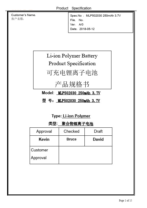
锂离子电池产品规格书 MLP502030 250mAh 3.7V说明书
History of specification规格书修订记录Date Contents Remarks 2018-05-12First issue A0Content/目录1.Scope/适用范围Page42.Cell Specification/电芯规格说明Page4/53.Battery/Cell performance test Criteria/电池性能标准Page6 3.1Appearance inspection by visual/外观目测Page6 3.2Environmental test condition/外界环境条件Page6 3.3Electrical characteristics/电气特性Page6 3.4Mechanical characteristics/机械特性Page73.5Safety performance/安全性能Page7/84.Cell initial Dimensions/电芯初始尺寸Page84.2Picture of assembled battery组合电池图5.Protection Circuit保护电路5.1PCM parameter PCM参数6.Circuit topology Drawing and PIN Explanation电路布线图和焊盘说明6.1PCM BOM保护板物料清单6.2Assembled cell parameters包装后电芯组参数附录Page9 Page9 Page9 Page10 Page10 Page101.Scope/适用范围The specification shall be applied to Li-ion Polymer rechargeable battery pack of MLP502030 250mAh3.7V,which is manufactured.本规格书适用于公司生产的MLP502030250mAh3.7V可充电聚合物锂离子电池.2.Cell Specification/电芯产品规格No.Item项目Specification性能1Rated Capacity额定容量250mAh,0.2C discharging2Minimum Capacity最小容量250mAh,0.2C discharging3Normal Voltage标称电压3.70V4O.C.V出厂电压 3.80-4.2V5Charge Ending Voltage充电截止电压4.20±0.03V6Discharge Ending Voltage放电截止电压3.0V7Standard charging method标准充电方式0.5C constant current charge to 4.2V,then constantvoltage4.2V charge till charged current declines to≤0.01C,0℃~45℃8Charge current充电电流Standard charge:0.2CRapid charge:1.0C9charging Time充电时间Standard charge:5.5~6.5hRapid charge:1.5~2.5h10Max.Charging Current最大充电电流1.0C(5℃~+45℃)11Standard dischargingCurrent标准放电电流0.2C constant current discharge to3.0V.10℃~+60℃12Max.Discharging Current最大放电电流1.0C(10℃~+60℃)13Operating environment工作环境Charging:0℃-45℃,65%±25%RHDischarging:10℃-60℃,65%±25%RH14Cell Impedance单电芯内阻<140mohm,(4.2V AC1KHz measured)15Dimension of Single Cell单电芯尺寸Thickness Max5.0mmWidth Max20.5mmHeight Max30.5mm3.Picture of single cell 单体电芯图Fig.(1)The Dimension of Single Cell图(1)单体电池尺寸图厚度T 宽度W 长度L L1W1E 5.0±0.120.0±0.530.0±0.56.5±1.52.0-3.07.0±1.5UNIT 单位:MM4.Picture of assembled battery组合电池图Fig.(2)The Dimension of Assembled Battery图(2)组合电池外形尺寸图厚度T 宽度W 长度L 线径Ø线型插头型号5.0±0.120.0±1.033.0±1.00.9UL1007/24#XH2.54-2P备注:UNIT 单位:MM5.产品规格及电气参数Product Specification and Electrical Parameters序号Item项目Specification性能1Assembled Mode组合方式1P2Normal Capacity标称容量≥250mAh,0.2C discharging3Normal Voltage标称电压3.7V4Impedance成品内阻<240mohm,(100%charge AC1KHz measured)5Assembly Dimension装配尺寸Thickness Max5.1mmWidth Max21.0mmHeight Max33.0mm4.Battery/Cell performance test Criteria/电池性能标准4.1Appearance inspection by visual/外观目测There shall be no such defect as rust,leakage,which may adversely affect commercial value of battery.电池外观应没有锈渍、污渍、漏液等影响商业价值的缺陷存在。
PSL621U系列线路保护装置

PSL 621U 系列线路保护装置技术性能及指标额定电气参数名称直流电源交流电压交流电流额定频率同期电压额定电气参数 220V 或 110V(订货请注明),允许工作围:(80%~115%)额定直流电压 100V 或者100 / 3 V (额定电压 Un) 5A 或 1A(额定电流 In,订货请注明) 50Hz(60Hz 时订货请注明) 100V 或100 / 3 V(有重合闸时使用,保护自适应) 2 倍额定电流,连续工作交流电流回路 6 过载能力交流电压回路 10 倍额定电流,允许 10s 40 倍额定电流,允许 1s 1.2 倍额定电压,连续工作 1.4 倍额定电压,允许 10s 正常时,不大于 50W 动作时,不大于 80W 不大于 0.5VA/相(额定电压时)不大于 0.5VA/相(In=5A 时)不大于 0.3VA/相(In=1A 时) 24V 24V 220V 或 110V直流回路 7 功率消耗交流电压回路交流电流回路通信接口模件的输入状态量电平 8 状态量电平 GPS 对时脉冲输入电平开入模件输入状态量电平主要技术性能及指标保护主要技术指标名称交流输入回路精确工作围模拟量测量精度整组动作时间相电压: 0.2 V~120V 同期电压:0.2 V~120V 电流: 0.04In~40In 主要技术指标误差:不超过±5% 差动保护:全线速动时间不大于 25ms 距离Ⅰ段 (0.7 倍整定值)动作时间:小于 25ms 相间电流突变量启动元件:整定围 0.04A~5A 零序电流辅助启动元件:整定围 0.04A~200A 不大于 5% 暂态超越不大于 5%的最小整定二次侧阻抗值为0.1Ω(短路残压大于 0.5V) 金属性三相故障时,不大于±2% 检同期元件角度误差:不大于±3 度启动元件暂态超越最小整定阻抗(不包括因装置外部原因造成的误差) 测距误差(不包括因装置外部原因造成的误差) 自动重合闸PSL 621U 系列线路保护装置(智能站)说明书 2.2.2 测控主要技术指标序号 1 2 3 4 5 6 7 8 名称采样回路精确工作围电流电压精度功率精度频率精度 SOE 分辨率遥信传输延时遥控响应时间遥测传输延时电压:电流: 0.2 V~不超过 0.2% 不超过0.5% ±0.01Hz ≤1ms ≤1s ≤1s ≤3s2.2.3 光纤接口 (1) 远方保护接口序号 1 2 3 4 名称光纤种类光发射管光纤接口发送功率光接收器 5 6 7 接收灵敏功率传输距离光接收器饱和光功率单模,波长 1310nm 激光二极管(LD) FC-PC -3~-10dBm Pin Diode ≤-36dBm 专用光纤≤50km > -3dBm 光纤接口参数单模,波长 1550nm 激光二极管(LD) FC-PC ≥-1dBm Pin Diode ≤-36dBm 工程需要可到 100km > -3dBm注:当采用专用光纤通道传输时,在传输距离大于 50km,接收功率不够时(接收裕度小于 3~10dB),需在订货时注明,配用 1550nm 激光器件。
1435-2;1431-1;1431-2;1420-1;1420-2;中文规格书,Datasheet资料

M I C R O J A C K S98density packaging•Beryllium Copper multi-spring contact maintains retention after multiple insertions•Ideal for mounting transistors,re-sistors,diodes,IC’s and similar miniature components•Custom micro jacks manufactured to your specifications •Other platings available upon request.016 [0.41].083[2.11].055[1.40]L3-FINGER CLOSED ENTRY CONTACT.038[0.96].038[0.96]HEX ..020[0.50].130 [3.3].095 [2.4]L.072[1.9].045[1.14]4-FINGER CLOSED ENTRY CONTACT.056[1.42].049[1.24].041[1.04].063[1.60]4-FINGER CLOSED ENTRY CONTACT.205[5.2].089[2.23].248[6.3]4-FINGER CLOSED ENTRY CONTACT.120[3.1].259[6.6].233[5.9].060[1.52]DIA..014[0.4].077[2.0]DIA..015(.38)-.021(.53)PIN -SOLDER MOUNT.015(.38)-.021(.53)PIN -PRESS FIT.015(.38)-.025(.64)PIN -TAPER-FIT.022(.56)-.032(.81)PIN -SOLDER MOUNT.015(.38)-.025(.64)PIN -SOLDER MOUNT.015(.38)-.025(.64)PIN -SOLDER MOUNT.022(.56)-.034(.86)PIN -PRESS FIT.025(.64)-.037(.94)PIN -PRESS FIT.025(.64)-.037(.94)PIN -SOLDER MOUNT.055[1.39].072[1.83].016 [0.41]4-FINGER CLOSED ENTRY CONTACT.093 [2.36].142[3.6].161[4.1]RoHS NON-RoHS Mtg.GOLD/GOLD TIN/TIN TIN/GOLD L Hole CAT.NO.CAT.NO.CAT.NO.Length Dia.1411-11431-11420-1.140(3.6).0421411-21431-21420-2.170(4.3)(1.07)RoHS NON-RoHS Mtg.GOLD/GOLD TIN/TIN TIN/GOLD L Hole CAT.NO.CAT.NO.CAT.NO.Length Dia.1412-11432-11468-1.140(3.6).0401412-21432-21468-2.170(4.3)(1.02)1412-31432-31468-3.282(7.2)RoHS NON-RoHS Mtg.GOLD/GOLD TIN/TIN TIN/GOLD L Hole CAT.NO.CAT.NO.CAT.NO.Length Dia.1415-11435-11469-1.160(4.1).0551415-21435-21469-2.190(4.8)(1.40)RoHS NON-RoHS Mtg.GOLD/GOLD TIN/TIN TIN/GOLD Hole CAT.NO.CAT.NO.CAT.NO.Dia.169316941695.063(1.60)RoHS NON-RoHS Mtg.GOLD/GOLD TIN/TIN TIN/GOLD Hole CAT.NO.CAT.NO.CAT.NO.Dia.141314331470.059(1.50)RoHS NON-RoHS Mtg.GOLD/GOLD TIN/TIN TIN/GOLD Hole CAT.NO.CAT.NO.CAT.NO.Dia.160316061607.052(1.32).061 [1.55].015[0.38].028[0.71].091 [2.3].086[2.2].170[4.3].200[5.1].070 [1.78]KNURL6-FINGER CLOSEDENTRY CONTACT6-FINGER CLOSED ENTRY CONTACT.057[1.45].077[1.96].083[2.11].025[0.7]L.025(.64)-.037(.94)PIN -SOLDER MOUNTRoHS NON-RoHS Mtg.GOLD/GOLD TIN/TIN TIN/GOLD Hole CAT.NO.CAT.NO.CAT.NO.Dia.141614361471.067(1.70)RoHSNON-RoHS Mtg.GOLD/GOLD TIN/TIN TIN/GOLD L Hole CAT.NO.CAT.NO.CAT.NO.Length Dia.1626-11614-11619-1.095(2.4).0621626-21614-21619-2.105(2.7)(1.57)1626-31614-31619-3.155(3.9).045 [1.14].062[1.57].090[2.29]6-FINGER CLOSED ENTRY CONTACT.080 [2.03].083 [2.11].022(.56)-.034(.86)PIN -SOLDER MOUNTRoHS NON-RoHS Mtg.GOLD/GOLD TIN/TIN TIN/GOLD Hole CAT.NO.CAT.NO.CAT.NO.Dia.165816591673.065(1.65).128[3.3].168[4.3].040 [1.02].092 [2.34].065 [1.65]L.200[5.1].230[5.9]4-FINGER CLOSED ENTRY CONTACT.125 [3.2].032(.81)-.046(1.17)PIN -SWAGE MOUNTRoHS NON-RoHS Mtg.GOLD/GOLD TIN/TIN TIN/GOLD Hole CAT.NO.CAT.NO.CAT.NO.Dia.359035913592.065(1.65)RoHS NON-RoHS Mtg.GOLD/GOLD TIN/TIN TIN/GOLD Hole CAT.NO.CAT.NO.CAT.NO.Dia.169716981699.063(1.60)RoHSNON-RoHS Mtg.GOLD/GOLD TIN/TIN TIN/GOLD L Hole CAT.NO.CAT.NO.CAT.NO.Length Dia.1419-11439-11478-1.062(1.6).0691419-21439-21478-2.094(2.4)(1.75)PLATING OPTIONSCONTACT PLATING BODY SPRING RoHS Gold/Gold Gold Gold Compliant Tin/Tin Tin/Lead Tin/Lead Non-CompliantTin/GoldTin/LeadGoldBody:Brass,ASTM-B16Spring:Beryllium Copper(QQ-C-533).057[1.45]HEX.057[1.45]DIA..200[5.1].020[0.52].078[1.98]DIA.6-FINGER CLOSED ENTRY CONTACT.165[4.2].078[1.98].040[1.02].090[2.29].040[1.02].062[1.57].210[5.3].187[4.7].180[4.6]6-FINGER CLOSED ENTRY CONTACTRoHS Plating:Gold:.000010per MIL-G-45204(RoHS Compliant)Tin/Lead:.000200to.000300per MIL-T-10727,Type 1(Non-RoHS Compliant).038[0.96]3-FINGER CLOSED ENTRY CONTACTL .055[1.40].083[2.11].016[0.41]RoHS Tel (718)956-8900•Fax (718)956-9040(800)221-5510•kec@31-0720th Road –Astoria,NY 11105-2017RoHS COMPLIANT ~ISO 9001CERTIFIED®分销商库存信息:KEYSTONE-ELECTRONICS1435-21431-11431-2 1420-11420-21470 1411-11411-21435-1 1469-11469-21614-3 1468-11468-21607 16951619-31606 169414711699 1415-11415-21413 359116981659 359216031432-1 1432-21432-31673 1468-316581697 1614-214161619-1 1619-216933590 1626-11626-21626-3 1412-11412-21412-3 1439-11439-21478-2 1419-21419-1。
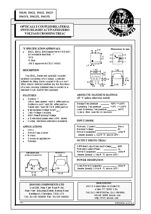
IS621SM中文资料
R= 10k
D.U.T.
X100 SCOPE PROBE
Vmax = 400V 252 V dv/dt= 0.63 Vmax
On-state voltage VTM (V)
τRC
τRC
=
378 τRC
04/03/03
DB92005m-AAS/A5
Fig.5 On-state Voltage vs. Ambient Temperature
3.0 I TM= 100mA
Fig.6 Holding Current vs. Ambient Temperature
1 VP= 6V
On-state voltage VTM(V)
2.2 1.8 1.4 1.0 20 40 60 80
OPTION SM
SURFACE MOUNT
OPTION G
7.62
0.6 0.1 10.46 9.86
1.25 0.75
0.26 10.16
Total Power Dissipation 250mW (derate linearly 2.94mW/0C above 250C)
ISOCOM COMPONENTS LTD Unit 25B, Park View Road West, Park View Industrial Estate, Brenda Road Hartlepool, Cleveland, TS25 1YD Tel: (01429) 863609 Fax :(01429) 863581
100
Static dv/dt Test Circuit
+ 400 Vdc
On-state current ITM (mA)
RTEST CTEST
电线电缆和软线参考标准
电线电缆和软线参考标准REFERENCESTANDRDFORELECTRICAL WIRESCABLESAND FLEXIBLE CORDSUL1581-2001上海电缆研究所电线电缆信息中心前言A:本标准包含美国保险商实验所(UL)产品的跟踪服务时涉及的产品基本要求,些产品受下列条文的限制,且处于本标准适用范围之内。
这些要求是以可信的工程原理,研究成果。
试验数据和现场经验以及对制造安装和使用的问题的评估为依据而制定的。
这些依据来自向制造商,用户检验机构以及其它具有专业经验的人员咨询或是从他们处获的情报。
上述对产品的要求可能由于经验丰富的研究人员深入而必须或是有必要进行修订。
B:满足本标准对产品的要求是制造商产品继续获得UL认证的条件之一。
C:符合本标准条文的产品如果经检验发现还具有其它有损于本标准的安全水平的性能,则不一定认为符合本标准。
D:采用本标准规定不同的材料制成的产品或是具有与本标准规定不同的结构的产品,可按本标准的要求的含义进行检验和测试,如果性能基本相同,则认为该产品符合本标准。
E:UL按其宗旨履行职能时,不为制造商或是任何一方担当或开脱责任。
UL 的意见和调查结果是代表一种充分考虑到UL标准制定时实际运行的必要限制和工艺水平专业性评定,UL对此不负任何责任。
如果因使用,解释UL标准或是其它依据而造成的损失包括重大损失,UL不负任何责任和义务。
F:本UL标准规定的许多试验本身具有一定的危险性,因此在做些试验时应采取恰当的人员和设备防护措施。
导引1:范围1.1本标准包含橡皮绝缘电线电缆(UL44)热塑性料绝缘电线电缆(UL83)软线装置线(UL62)和用户引入电缆(UL854)等标准对于导体,绝缘,护套及其它护层的要求细则以及对于试样制备。
样品选取,温度处理和测量与计算方法的要求细则。
本标准的条文也被其它标准所引用。
1.2对于特定型号的电线电缆或软线的专用材料、结构、性能和标志的要求,载于相应的成品电缆标准中,本参考标准不包含这些内容。
68112;68111;68110;中文规格书,Datasheet资料
E
F
*Glove should be grounded to verify dissipation of static charges. Use Desco 09480 coil cord or equivalent to ground.
Made in America
HOT GLOVES, STATIC DISSIPATIVE
DESCO WEST:3651 WALNUT AVE., CHINO, CA 91710 WEB SITE: PHONE (909) 627-8178 FAX (909) 627-7449 DESCO EAST: ONE COLGATE WAY, CANTON, MA 02021-1407 PHONE (781) 821-8370 FAX (781) 575-0172
DRAWING NUMBER 68110
DATE: January 2009
© 2009 DESCO INDUSTRIES INC.
Employee Owned
分销商库存信息:
DESCO 68112 68111 68110
A
B
C
D
ITEM # SIZE 68110 68111 68112 Large Medium Small
CUFF COLOR Brown Blue Beige
E 6" 6" 6"
F 3 1/8" 2 3/4" 2 1/2"
Glove Laundering For proper operation, the ESD Gloves must be laundered periodically. Woolite works well. Liquid detergents are better than dry in that there is less caking and frictional wear. Launder glove in cool or warm water, tumble dry with low heat or hang dry. Machine washing works well if using a standard house machine on gentle cycle. It is not recommended to launder these gloves in heavy industrial laundry machines as it will lead to premature wear. Gloves should be tumbled dry using low heat. DO NOT BLEACH. After laundering, verify RTT <107 ohms.
RH6015-C(D)原厂规格书
单通道触摸感应开关RH6015-C(D)规格书Revision2.52019-06-03目录1.简介 (3)2.特点 (3)3.封装引脚示意图及模式 (4)3.1引脚示意图 (4)3.2默认输出模式 (4)4.订购信息 (5)5.功能描述 (5)5.1输出有效电平配置(AHLB) (5)5.2快速/低功耗模式 (6)5.3保持/同步模式(TOG) (6)5.4最大开启时间 (6)6.应用电路图 (6)7.PCB设计注意事项 (7)8.电气参数 (8)8.1最大绝对额定值 (8)8.2DC电气参数 (8)9.封装信息(SOT23-6) (9)10.封装信息(DFN6) (11)1.简介RH6015是一款内置稳压模块的单通道电容式触摸感应控制开关IC,可以替代传统的机械式开关。
RH6015可在有介质(如玻璃、亚克力、塑料、陶瓷等)隔离保护的情况下实现触摸功能,安全性高。
RH6015内置高精度稳压、上电复位、低压复位、硬件去抖、环境自适应算法等多种有效措施,大大提高自身抗干扰性能。
RH6015可通过外部引脚配置成多种工作模式,可广泛应用于灯光控制、电子玩具、消费电子、家用电器等产品中。
RH6015C[A],CMOS输出,SOT23-6封装。
RH6015CL(F),CMOS输出,DFN6封装。
RH6015D[A],NMOS开漏输出,SOP23-6封装。
2.特点∙工作电压:2.3V~5.5V∙最高功耗工作电流5.0uA@3V,低功耗模式工作电流2.5uA@3V∙内置高精度稳压模块∙上电0.5s快速初始化∙环境自适应功能,可快速应对触摸上电等类似应用场景∙可靠的上电复位(POR)及低压复位(LVR)性能∙芯片内置去抖动电路,有效防止由外部噪声干扰导致的误动作∙通过外部引脚配置快速/低功耗模式、同步/保持模式∙可通过外部引脚设置高/低电平有效输出、最大开启时间∙封装:SOT23-6、DFN63.封装引脚示意图及模式3.1引脚示意图图1RH6015C[A]/RH6015D[A](SOT23-6)引脚示意图表图2RH6015CL/RH6015CF(DFN6)引脚示意图表I-P L/I-P H:带内部下拉/上拉电阻的CMOS输入OD:CMOS开漏输出,无保护二极管O:推挽型CMOS输出I/O:CMOS输入/输出P:电源/地3.2默认输出模式可配置:指该封装上有相应模式的配置管脚引出,具体见5.功能描述。
MLZ系列多层镍酸盐电感器说明书
Inductors for decoupling circuits Multilayer ferriteMLZ series (for automotive)MLZ2012 typeFEATURESAPPLICATIONtable memory audio devices, navigation systems, PNDs, WLANs, SSDsPART NUMBER CONSTRUCTIONCHARACTERISTICS SPECIFICATION TABLE*1 Current assumed when inductance ratio has decreased by 50% max..*2 Current assumed when temperature has risen to 20°C typ. (reference value). Operating temperature environment at this time: 105°C max.Measurement equipmentEquivalent measurement equipment may be used.MLZ2012M100HTD25Series nameL×W×H dimensions Product internal codeInductanceCharacteristic typePackaging styleInternal code2.0×1.25×0.85 mm 2.0×1.25×1.25 mm(µH)TypeLThickness L measuring conditions DC resistance Rated current Reference value Part No.TFrequencyCurrent(Isat)*1(Itemp)*2(µH)Tolerance (mm)(MHz)(mA)(Ω)±30%(mA)max.(mA)typ.Ultra-largecurrent1.0 ±20% 1.2520.10.10 700800MLZ2012M1R0HTD251.5 ±20% 1.2520.10.14 550700MLZ2012M1R5HTD252.2 ±20% 1.2520.10.16 400600MLZ2012M2R2HTD253.3 ±20% 1.2520.10.20 350500MLZ2012M3R3HTD254.7 ±20% 1.2520.10.34 300400MLZ2012M4R7HTD256.8 ±20% 1.2520.10.40 220350MLZ2012M6R8HTD2510±20% 1.2520.10.68 200300MLZ2012M100HTD25Highfrequency0.10±20%0.8525 1.00.0710001150MLZ2012DR10DTD250.22±20%0.8525 1.00.13800900MLZ2012DR22DTD250.47±20% 1.2525 1.00.18550700MLZ2012DR47DTD25Measurement item Product No.ManufacturerL 4294A+16034G Keysight T echnologies DC resistance Type-7561Y okogawaAEC-Q200CHARACTERISTICS SPECIFICATION TABLE*1 Current assumed when inductance ratio has decreased by 50% max..*2 Current assumed when temperature has risen to 20°C typ. (reference value). Operating temperature environment at this time: 105°C max.Measurement equipmentEquivalent measurement equipment may be used.TypeLThickness L measuring conditions DC resistance Rated current Reference value Part No.TFrequencyCurrent(Isat)*1(Itemp)*2(µH)Tolerance (mm)(MHz)(mA)(Ω)±30%(mA)max.(mA)rgecurrent 1.00±20%0.8510 1.00.10280900MLZ2012A1R0WTD251.50±20%0.8510 1.00.13250750MLZ2012A1R5WTD252.20±20%0.8510 1.00.15210650MLZ2012A2R2WTD253.30±20%0.8510 1.00.34200450MLZ2012A3R3WTD254.70±20%0.8520.10.30180500MLZ2012M4R7WTD256.80±20% 1.2520.10.40160400MLZ2012M6R8WTD2510.0±20% 1.2520.10.47150350MLZ2012M100WTD2515.0±20% 1.2520.10.95120250MLZ2012M150WTD2522.0±20% 1.2520.1 1.25100220MLZ2012P220WTD2522.0±20% 1.2520.1 2.060220MLZ2012M220WTD2533.0±20% 1.2520.1 2.6055190MLZ2012M330WTD2547.0±20% 1.2520.1 3.7050170MLZ2012M470WTD25Lowresistance 1.00±20%0.8520.10.062201150MLZ2012N1R0LTD251.50±20%0.8520.10.10190900MLZ2012N1R5LTD252.20±20%0.8520.10.12170800MLZ2012N2R2LTD253.30±20%0.8520.10.15130750MLZ2012N3R3LTD254.70±20%0.8520.10.18130600MLZ2012N4R7LTD256.80±20%0.8520.10.25110550MLZ2012N6R8LTD2510.0±20% 1.2520.10.30110500MLZ2012N100LTD2515.0±20% 1.2520.10.4790350MLZ2012N150LTD2522.0±20% 1.2520.10.6770300MLZ2012N220LTD25100.0±20% 1.2520.1 3.5030140MLZ2012N101LTD25Measurement item Product No.ManufacturerL 4294A+16034G Keysight T echnologies DC resistance Type-7561Y okogawaL FREQUENCY CHARACTERISTICS H CHARACTERISTIC PRODUCTMeasurement equipmentProduct No.ManufacturerE4991A+16192 Keysight T echnologiesEquivalent measurement equipment may be used.L FREQUENCY CHARACTERISTICS D CHARACTERISTIC PRODUCTMeasurement equipmentProduct No.ManufacturerE4991A+16192A Keysight T echnologiesEquivalent measurement equipment may be used.L FREQUENCY CHARACTERISTICS W CHARACTERISTIC PRODUCTMeasurement equipmentProduct No.ManufacturerE4991A+16192 Keysight T echnologiesEquivalent measurement equipment may be used.L FREQUENCY CHARACTERISTICS L CHARACTERISTIC PRODUCTMeasurement equipmentProduct No.ManufacturerE4991A+16192 Keysight T echnologiesEquivalent measurement equipment may be used.INDUCTANCE VS. DC BIAS CHARACTERISTICS H CHARACTERISTIC PRODUCTMeasurement equipmentProduct No.Manufacturer4291B+16200A+16192A Keysight T echnologiesEquivalent measurement equipment may be used.INDUCTANCE VS. DC BIAS CHARACTERISTICS D CHARACTERISTIC PRODUCTMeasurement equipmentProduct No.Manufacturer4291B+16200A+16192A Keysight T echnologiesEquivalent measurement equipment may be used.INDUCTANCE VS. DC BIAS CHARACTERISTICS W CHARACTERISTIC PRODUCTMeasurement equipmentProduct No.Manufacturer4291B+16200A+16192A Keysight T echnologiesEquivalent measurement equipment may be used.INDUCTANCE VS. DC BIAS CHARACTERISTICS L CHARACTERISTIC PRODUCTMeasurement equipmentProduct No.Manufacturer4291B+16200A+16192A Keysight T echnologiesEquivalent measurement equipment may be used.IMPEDANCE FREQUENCY CHARACTERISTICS H CHARACTERISTIC PRODUCTMeasurement equipmentProduct No.ManufacturerE4991A+16192A Keysight T echnologiesEquivalent measurement equipment may be used.IMPEDANCE FREQUENCY CHARACTERISTICS D CHARACTERISTIC PRODUCTMeasurement equipmentProduct No.ManufacturerE4991A+16192A Keysight T echnologiesEquivalent measurement equipment may be used.IMPEDANCE FREQUENCY CHARACTERISTICS W CHARACTERISTIC PRODUCTMeasurement equipmentProduct No.ManufacturerE4991A+16192A Keysight T echnologiesEquivalent measurement equipment may be used.IMPEDANCE FREQUENCY CHARACTERISTICS L CHARACTERISTIC PRODUCTMeasurement equipmentProduct No.ManufacturerE4991A+16192A Keysight T echnologiesEquivalent measurement equipment may be used.MLZ2012 type SHAPE & DIMENSIONSt=0.85mm t=1.25mmRECOMMENDED LAND PATTERNRECOMMENDED REFLOW PROFILEPACKAGING STYLETEMPERATURE RANGE, INDIVIDUAL WEIGHT *Operating temperature range includes self-temperature rise.**The storage temperature range is for after the assembly.Dimensions in mmDimensions in mmType A B KMLZ2012t=0.85 1.5±0.2 2.3±0.2 1.1 max. t=1.25 1.5±0.2 2.3±0.2 1.5 max.Package quantity t=0.85mm4000 pcs/reel t=1.25mm2000 pcs/reelTypeOperatingtemperature range*Storagetemperature range**Individualweightt=0.85mm–55 to +125 °C–55 to +125 °C10 mgt=1.25mm–55 to +125 °C–55 to +125 °C14 mgDimensions in mmREMINDERS FOR USING THESE PRODUCTSBefore using these products, be sure to request the delivery specifications.SAFETY REMINDERSPlease pay sufficient attention to the warnings for safe designing when using this products.The storage period is within 12 months. Be sure to follow the storage conditions (temperature: 5 to 40°C, humidity: 10 to 75% RH or less).If the storage period elapses, the soldering of the terminal electrodes may deteriorate.Do not use or store in locations where there are conditions such as gas corrosion (salt, acid, alkali, etc.).Before soldering, be sure to preheat components.The preheating temperature should be set so that the temperature difference between the solder temperature and chip temperature does not exceed 150°C.Soldering corrections after mounting should be within the range of the conditions determined in the specifications.If overheated, a short circuit, performance deterioration, or lifespan shortening may occur.When embedding a printed circuit board where a chip is mounted to a set, be sure that residual stress is not given to the chip due to the overall distortion of the printed circuit board and partial distortion such as at screw tightening portions.Self heating (temperature increase) occurs when the power is turned ON, so the tolerance should be sufficient for the set thermal design.Carefully lay out the coil for the circuit board design of the non-magnetic shield type.A malfunction may occur due to magnetic interference.Use a wrist band to discharge static electricity in your body through the grounding wire.Do not expose the products to magnets or magnetic fields.Do not use for a purpose outside of the contents regulated in the delivery specifications.The products listed on this catalog are intended for use in general electronic equipment (AV equipment, telecommunications equip-ment, home appliances, amusement equipment, computer equipment, personal equipment, office equipment, measurement equip-ment, industrial robots) under a normal operation and use condition.The products are not designed or warranted to meet the requirements of the applications listed below, whose performance and/or qual-ity require a more stringent level of safety or reliability, or whose failure, malfunction or trouble could cause serious damage to society,person or property.If you intend to use the products in the applications listed below or if you have special requirements exceeding the range or conditions set forth in the each catalog, please contact us.(1) Aerospace/aviation equipment(2) T ransportation equipment (electric trains, ships, etc.)(3) Medical equipment(4) Power-generation control equipment (5) Atomic energy-related equipment (6) Seabed equipment(7) T ransportation control equipment(8) Public information-processing equipment (9) Military equipment(10) Electric heating apparatus, burning equipment (11) Disaster prevention/crime prevention equipment(12) Safety equipment(13) Other applications that are not considered general-purposeapplicationsWhen designing your equipment even for general-purpose applications, you are kindly requested to take into consideration securing pro-tection circuit/device or providing backup circuits in your equipment.REMINDERS。
Eaton C621 电源设备说明说明书
Eaton C621Eaton Moeller series Luxury finish range (COPA) - Wiring Devices. Socket outlet, 13A, 1G, 2p, switched, white interiorGeneral specificationsEaton Moeller series Luxury finish range (COPA) - Wiring DevicesC621C621501082611668240 mm 86 mm 86 mm 0.074 kg RoHS conformBS 1363-2Product NameCatalog NumberModel Code EANProduct Length/Depth Product Height Product Width Product Weight Compliances Certifications13 A125 mm6.5 mmMattFlush mounted (plaster)White insert13 ADuroplast25 mm50 HzThermoplasticEarth on strap = 2.5 mm² (3x) or 4 mm² (1x) or 6 mm² (1x) L, N & E in base = 2.5 mm² (4x) or 4 mm² (2x) or 6 mm² (1x)Child-protectionLoop through functionOn/Off switch0eaton-us-power-defense-flyer-br013004en-en-us.pdf eaton-circuit-breakers-bzm-catalog-w1230-7594-gb-int.pdf eaton-xchargein-installation-manual-v1.01-en-us.pdfNominal currentNumber of unitsNumber of active pins (round) Recommended back box depth - min Front plate depthSurface finishingMounting methodCOPA interiorAmperage RatingMaterial qualityBuilt-in installation box depth - min Frequency rating - maxFront plate materialTerminal capacity (LN and E)Fitted with:Number of active pins (flat)Fixing centers BrochuresCatalogsInstallation instructions60.3 mmConnection typeScrewed terminalRocker colorWhiteNumber of phases2Voltage rating250 V ACImprint/indicationOtherHead styleCombination headFault current rating250 mASpecial featuresZinc Coated Steel with clear PassivationSwitch typeDouble poleDegree of protection (IP)IP20Front plate/module dimensions84 mm x 84 mmNominal voltage - max240 VColorWhiteFeaturesHalogen freeProtective contactMaterialPlasticUreaFront plate color/finishingWhiteNumber of gangs1Eaton Corporation plc Eaton House30 Pembroke Road Dublin 4, Ireland © 2023 Eaton. All Rights Reserved. Eaton is a registered trademark.All other trademarks areproperty of their respectiveowners./socialmediaGraySilver Nickel0Copa Sockets, switched Mounting with screw 0Untreated Thermoplastic No special power supply British Standard150 HzZinc coated steelBase color Contact material Number of modules (module system)TypeFastening type RAL-number (Akin)Surface protection Base material Special power supply ModelNumber of socket outlets (switchable)Frequency rating - min Terminal material。
- 1、下载文档前请自行甄别文档内容的完整性,平台不提供额外的编辑、内容补充、找答案等附加服务。
- 2、"仅部分预览"的文档,不可在线预览部分如存在完整性等问题,可反馈申请退款(可完整预览的文档不适用该条件!)。
- 3、如文档侵犯您的权益,请联系客服反馈,我们会尽快为您处理(人工客服工作时间:9:00-18:30)。
D H
Temperature Range Weight Dimensions
*1 Nominal capacity is determined to an end voltage of 2.0V when the battery is allowed to discharge at a standard current level at 23oC. *2 Current value is determined so that 50% of the nominal capacity is obtained with an end voltage of 2.0V at 23 oC. *3 Current value for obtaining 2.0V cell voltage when 15sec. pulse is applied at 50% discharge depth at 23 oC.
Typical Characteristics
Temperature Characteristics of ML621
3.5
Discharge Characteristics after storage of ML621
3.5
After 20days storage at 60oC
3.0
3.0
Cell Voltage(V)
3.0
5.0
2.5
4.0
2.0
3.0
Charge Condition:3.0V 50hour(R=1kohm) Discharge Condition:5.6kohm 1Mohm End voltage: 2.0V Temp.:23deg.C
5 10
1.5
Charge Condition:0.1mA 3.0Vcut Discharge Condition:0.1mA 5.5h Temp.: 23deg.C
0.0 1.0 2.0 3.0 4.0 5.0 6.0 7.0
1.0
1.0
Capacity (mAh)
Capacity (mAh)
Discharge Characteristics after Over-Discharge of ML621
3 .5
Continuous Charge Characteristics of ML621
3.5
After 30days discharged at 150kohm
3 .0
After 3.0V (R=1kohm) charge at 60oC for 20days
3.0
Cell Voltage (V)
Cell Voltage(V)
2 .5
2.5
2 .0
2.0
1 .5
Charge Condition:3.0V 50hour(R=1kohm) Discharge Condition:150kohm Temp.: 23deg.C
2.5
-20oCቤተ መጻሕፍቲ ባይዱ
2.0
23oC
60oC
Cell Voltage(V)
2.5
2.0
1.5
Charge Condition:3.0V 50hour(R=1kohm) Discharge Condition:150kohm
0.0 1.0 2.0 3.0 4.0 5.0 6.0 7.0
1.5
Charge Condition:3.0V 50hour(R=1kohm) Discharge Condition:150kohm Temp.: 23deg.C
Duration(hour)
Capacity (mAh)
Charge Characteristics of ML621
Charge/Discharge Cycle Characteristics of ML621
3.5
6.0
Cell Voltage at End of Discharge (V)
Discharge Capacity(mAh)
0 50 100 150 200 250 300 350 400 450 500
Load Resistance (kohm)
These are just measured data. Not guaranteed.
50
100
500
10 00
1.0
Cycle Number
Just measured data, not guaranteed.
Cell Type ML621 Specifications
Nominal Capacity*1 Nominal Voltage Standard Charge/Discharge Current Max. Discharge Current Charge/Discharge Cycle Characteristics Charging Method 5.8mAh 3.0V 0.015mA Continuous *2 0.5mA 1.5mA Pulse*3 Discharging Depth of 5% 3000 Discharging Depth of 20% 300 Constant Voltage Charge 3.1±0.15V Hight Temperature 2.95±0.15V -20oC-60oC 0.22g Diameter(D) 6.8mm Height(H) 2.1mm
0 10 0 20 0 3 00 4 00
1.5
Charge Condition:3.0V 20days(R=1kohm) at 60oC Discharge Condition:150kohm Temp.: 23deg.C
1.0 2.0 3.0 4.0 5.0 6.0 7.0
1 .0
1.0 0.0