A 40-GHZ frequency divider in 90nm
OPA404中文资料

*
*
*
*
*
*
*
*
*
*
*
*
*
*
*
*
*
*
*
*
*
*
*
*
*
*
*
–55
+125
*
*
*
*
*
UNITS
nV/√Hz nV/√Hz nV/√Hz nV/√Hz µVrms µVp-p fA, p-p fA/√Hz
µV µV µV/°C µV/°C dB dB dB
pA pA
pA pA
Ω || pF Ω || pF
V dB dB
®
OPA404
2
元器件交易网
ELECTRICAL (FULL TEMPERATURE RANGE SPECIFICATIONS)
At VCC = ±15VDC and TA = TMIN to TMAX unless otherwise noted.
OPA404AG, KP, KU
BIAS CURRENT Input Bias Current
KP, KU
VCM = 0VDC
OFFSET CURRENT Input Offset Current
KP, KUຫໍສະໝຸດ VCM = 0VDCIMPEDANCE Differential Common-Mode
VOTAGE RANGE Common-Mode Input Range Common-Mode Rejection
RL ≥ 2kΩ
Gain = 100 20Vp-p, RL = 2kΩ VO = ±10V, RL = 2kΩ Gain = –1, RL = 2kΩ CL = 100 pF, 10V Step
mt9043中文资料_数据手册_IC数据表

-40°C to +85°C
8kHz input reference signals
• Provides C1.5, C2, C4, C6, C8, C16, and C19
Description
(STS-3/OC3 clock divided by 8) output clock signals
• Provides 5 different styles of 8 KHz framing pulses
Applications
https:/// Stratum 4; and ETSI ETS 300 011. It will meet the jitter/wander tolerance, jitter transfer, intrinsic jitter,
frequency accuracy, capture range, phase change
1
Zarlink Semiconductor Inc. Zarlink, ZL and the Zarlink Semiconductor logo are trademarks of Zarlink Semiconductor Inc.
Copyright 2003, Zarlink Semiconductor Inc. All Rights Reserved.
11
38
12
37
13
36
14
35
15
34
16
33
17
32
18
31
19
30
20
29
21
28
22
27
23
26
24
25
ADF4158
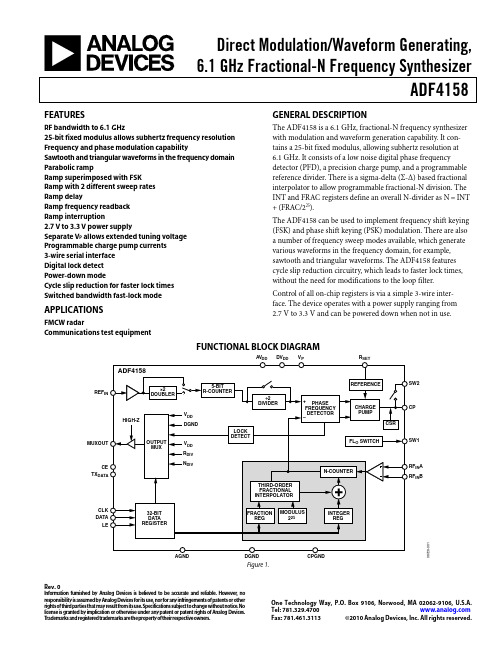
Direct Modulation/Waveform Generating,6.1 GHz Fractional-N Frequency SynthesizerADF4158Rev. 0Information furnished by Analog Devices is believed to be accurate and reliable. However , no responsibility is assumed by Analog Devices for its use, nor for any infringements of patents or other rights of third parties that may result from its use. Specifications subject to change without notice. No license is granted by implication or otherwise under any patent or patent rights of Analog Devices. T rademarks and registered trademarks are the property of their respective owners.O ne Technology Way, P.O. Box 9106, Norwood, MA 02062-9106, U.S.A.Tel: 781.329.4700 Fax: 781.461.3113 ©2010 Analog Devices, Inc. All rights reserved.FEATURESRF bandwidth to 6.1 GHz25-bit fixed modulus allows subhertz frequency resolution Frequency and phase modulation capabilitySawtooth and triangular waveforms in the frequency domain Parabolic rampRamp superimposed with FSK Ramp with 2 different sweep rates Ramp delayRamp frequency readback Ramp interruption2.7 V to3.3 V power supplySeparate V P allows extended tuning voltage Programmable charge pump currents 3-wire serial interface Digital lock detect Power-down modeCycle slip reduction for faster lock times Switched bandwidth fast-lock modeAPPLICATIONSFMCW radarCommunications test equipmentGENERAL DESCRIPTIONThe ADF4158 is a 6.1 GHz, fractional-N frequency synthesizer with modulation and waveform generation capability. It con-tains a 25-bit fixed modulus, allowing subhertz resolution at 6.1 GHz. It consists of a low noise digital phase frequencydetector (PFD), a precision charge pump, and a programmable reference divider. There is a sigma-delta (Σ-Δ) based fractional interpolator to allow programmable fractional-N division. The INT and FRAC registers define an overall N-divider as N = INT + (FRAC/225).The ADF4158 can be used to implement frequency shift keying (FSK) and phase shift keying (PSK) modulation. There are also a number of frequency sweep modes available, which generate various waveforms in the frequency domain, for example, sawtooth and triangular waveforms. The ADF4158 features cycle slip reduction circuitry, which leads to faster lock times, without the need for modifications to the loop filter. Control of all on-chip registers is via a simple 3-wire inter- face. The device operates with a power supply ranging from 2.7 V to 3.3 V and can be powered down when not in use.FUNCTIONAL BLOCK DIAGRAMDATA LETX DATACE CLK REF ININ A IN BMUXOUT08728-001Figure 1.ADF4158Rev. 0 | Page 2 of 36TABLE OF CONTENTSFeatures .............................................................................................. 1 Applications ....................................................................................... 1 General Description ......................................................................... 1 Functional Block Diagram .............................................................. 1 Revision History ............................................................................... 2 Specifications ..................................................................................... 3 Timing Specifications .................................................................. 4 Absolute Maximum Ratings ............................................................ 6 ESD Caution .................................................................................. 6 Pin Configuration and Pin Function Descriptions ...................... 7 Typical Performance Characteristics ............................................. 8 Circuit Description ......................................................................... 10 Reference Input Section ............................................................. 10 RF Input Stage ............................................................................. 10 RF INT Divider ........................................................................... 10 25-Bit Fixed Modulus ................................................................ 10 INT, FRAC, and R Relationship ............................................... 10 R-Counter .................................................................................... 10 Phase Frequency Detector (PFD) and Charge Pump ............ 11 MUXOUT and LOCK Detect ................................................... 11 Input Shift Registers ................................................................... 11 Program Modes .......................................................................... 11 Register Maps .................................................................................. 12 FRAC/INT Register (R0) Map .................................................. 14 LSB FRAC Register (R1) Map ................................................... 15 R-Divider Register (R2) Map .................................................... 16 Function Register (R3) Map ...................................................... 18 Test Register (R4) Map .............................................................. 20 Deviation Register (R5) Map .................................................... 21 Step Register (R6) Map .............................................................. 22 Delay Register (R7) Map ........................................................... 23 Applications Information .............................................................. 24 Initialization Sequence............................................................... 24 RF Synthesizer: A Worked Example ........................................ 24 Reference Doubler and Reference Divider ............................. 24 Cycle Slip Reduction for Faster Lock Times ........................... 24 Modulation .................................................................................. 25 Waveform Generation ............................................................... 25 Additional Features .................................................................... 27 Fast-Lock Timer and Register Sequences ............................... 30 Fast Lock: An Example .............................................................. 30 Fast Lock: Loop Filter Topology ............................................... 30 Spur Mechanisms ....................................................................... 31 Low Frequency Applications .................................................... 31 Filter Design—ADIsimPLL ....................................................... 31 PCB Design Guidelines for the Chip Scale Package .............. 31 Application of ADF4158 in FMCW Radar ................................. 32 Outline Dimensions ....................................................................... 33 Ordering Guide (33)REVISION HISTORY4/10—Revision 0: Initial VersionADF4158Rev. 0 | Page 3 of 36SPECIFICATIONSAV DD = DV DD = 2.7 V to 3.3 V , V P = AV DD to 5.5 V , AGND = DGND = 0 V , T A = T MIN to T MAX , dBm referred to 50 Ω, unless otherwise noted. Table 1.C Version 1 Parameter Min Typ Max Unit Test Conditions/Comments RF CHARACTERISTICS RF Input Frequency (RF IN ) 0.5 6.1 G Hz −10 dBm min to 0 dBm max; for lower frequencies, ensureslew rate (SR) > 400 V/μs−15 dBm min to 0 dBm max for 2 GHz to 4 GHz RF input frequencyREFERENCE CHARACTERISTICS REF IN Input Frequency 10 260 MHz For f < 10 MHz, use a dc-coupled CMOS-compatiblesquare wave, slew rate > 25 V/μs16 MHz If an internal reference doubler is enabled REF IN Input Sensitivity 0.4 AV DD V p-p Biased at AV DD /22 REF IN Input Capacitance 10 pF REF IN Input Current ±100 μA PHASE DETECTORPhase Detector Frequency 332 MHz CHARGE PUMP I CP Sink/Source Programmable High Value 5 mA With R SET = 5.1 kΩ Low Value 312.5 μA Absolute Accuracy 2.5 % With R SET = 5.1 kΩ R SET Range 2.7 10 kΩ I CP Three-State Leakage Current 1 nA Sink and source current Matching 2 % 0.5 V < V CP < V P – 0.5 V I CP vs. V CP 2 % 0.5 V < V CP < V P – 0.5 V I CP vs. Temperature 2 % V CP = V P /2 LOGIC INPUTS V INH , Input High Voltage 1.4 V V INL , Input Low Voltage 0.6 V I INH /I INL , Input Current ±1 μA C IN , Input Capacitance 10 pF LOGIC OUTPUTS V OH , Output High Voltage 1.4 V Open-drain output chosen; 1 kΩ pull-up to 1.8 V V OH , Output High Voltage V DD − 0.4 V CMOS output chosen I OH , Output High Current 100 μA V OL , Output Low Voltage 0.4 V I OL = 500 μA POWER SUPPLIES AV DD 2.7 3.3 V DV DD AV DD V P AV DD 5.5 V I DD 23 32 mAADF4158Rev. 0 | Page 4 of 36C Version 1Parameter Min Typ Max Unit Test Conditions/Comments NOISE CHARACTERISTICSNormalized Phase Noise Floor 4−213 dBc/Hz Phase Noise Performance 5 @ VCO output5805 MHz Output 6−93 dBc/Hz @ 5 kHz offset, 32 MHz PFD frequency1 Operating temperature for C version: −40°C to +125°C. 2AC-coupling ensures AV DD /2 bias. 3Guaranteed by design. Sample tested to ensure compliance. 4This figure can be used to calculate phase noise for any application. Use the formula –213 + 10 log(f PFD ) + 20 logN to calculate in-band phase noise performance as seen at the VCO output. 5The phase noise is measured with the EVAL-ADF4158EB1Z and the Agilent E5052A phase noise system. 6f REFIN = 128 MHz; f PFD = 32 MHz; offset frequency = 5 kHz; RF OUT = 5805 MHz; INT = 181; FRAC = 13631488; loop bandwidth = 100 kHz.TIMING SPECIFICATIONSAV DD = DV DD = SDV DD = 2.7 V to 3.3 V; V P = AV DD to 5.5 V; AGND = DGND = SDGND = 0 V; T A = T MIN to T MAX , dBm referred to 50 Ω, unless otherwise noted. Table 2. Write TimingParameter Limit at T MIN to T MAX (C Version) UnitTest Conditions/Comments t 1 20 ns min LE setup timet 2 10 ns min DATA to CLK setup time t 3 10 ns min DATA to CLK hold time t 4 25 ns min CLK high duration t 5 25 ns min CLK low duration t 6 10 ns min CLK to LE setup time t 7 20ns minLE pulse widthWrite Timing DiagramCLKDATALELE08728-026Figure 2. Write Timing DiagramADF4158Rev. 0 | Page 5 of 36Table 3. Read TimingParameter Limit at T MIN to T MAX (C Version)Unit Test Conditions/Comments t 1 20 ns min TX DATA setup time t 2 10 ns min DATA (on MUXOUT) to CLK setup time t 3 10 ns min DATA (on MUXOUT) to CLK hold time t 4 25 ns min CLK high duration t 5 25 ns min CLK low duration t 6 10ns min CLK to LE setup timeRead Timing DiagramCLKLE08728-226TX DATAFigure 3. Read Timing DiagramADF4158Rev. 0 | Page 6 of 36ABSOLUTE MAXIMUM RATINGST A = 25°C, GND = AGND = DGND = SDGND = 0 V , V DD = AV DD = DV DD = SDV DD , unless otherwise noted.Table 4. Parameter Rating V DD to GND −0.3 V to +4 V V DD to V DD −0.3 V to +0.3 V V P to GND −0.3 V to +5.8 V V P to V DD−0.3 V to +5.8 V Digital I/O Voltage to GND −0.3 V to V DD + 0.3 V Analog I/O Voltage to GND −0.3 V to V DD + 0.3 V REF IN , RF IN to GND−0.3 V to V DD + 0.3 V Operating Temperature RangeIndustrial (C Version)−40°C to +125°C Storage Temperature Range−65°C to +125°C Maximum Junction Temperature 150°C LFCSP θJA Thermal Impedance (Paddle Soldered) 30.4°C/W Reflow SolderingPeak Temperature260°C Time at Peak Temperature40 secStresses above those listed under Absolute Maximum Ratings may cause permanent damage to the device. This is a stressrating only; functional operation of the device at these or any other conditions above those indicated in the operational section of this specification is not implied. Exposure to absolute maximum rating conditions for extended periods may affect device reliability.ESD CAUTIONADF4158Rev. 0 | Page 7 of 36PIN CONFIGURATION AND PIN FUNCTION DESCRIPTIONS1CPGND NOTES1. THE LFCSP HAS AN EXPOSED PADDLE THAT MUST BE CONNECTED TO GND.2AGND 3AGND 4RF IN B 5RF IN A 6AV DDDATA LE MUXOUT SDV DD 14CLK 13CE7A V D D 8A V D D 9R E F I N 11S D G N D 12T X D A T A 10D G N D 1S W 22V P 3R S E T 4C P 0S W 19D V D D08728-003Figure 4. LFCSP Pin ConfigurationG GADF4158Rev. 0 | Page 8 of 36TYPICAL PERFORMANCE CHARACTERISTICS–160–140–120–100–80–60–401k10k100k1M10MP H A S E N O I S E (d B c /H z )FREQUENCY OFFSET (Hz)08728-035Figure 5. Phase Noise at 5805 MHz, PFD = 32 MHz, Loop Bandwidth = 100 kHz5.785.795.805.815.825.835.845.855.86–0.025–0.015–0.0050.0050.0150.025F R E Q UE N C Y (G H z )TIME (s)08728-036Figure 6. Triangular Waveform, PFD = 32 MHz, INT = 181, FRAC = 0, DEV Offset = 4, DEV Word = 20972, Step Word = 200, CLK DIV = 10,MOD Divider = 1255.755.775.795.815.835.855.87–0.010–0.00500.0050.010F R E Q U EN C Y (G H z )TIME (s)08728-037Figure 7. Sawtooth Waveform, PFD = 32 MHz, INT = 181, FRAC = 0, DEV Offset = 4, DEV Word = 20972, Step Word = 200, CLK DIV = 10,MOD Divider = 125 5.765.775.785.795.805.815.825.835.845.855.865.87F R E Q U E N C Y(G H z )TIME (s)–0.010–0.00500.0050.01008728-039Figure 8. Delay Between Ramps for Sawtooth Waveform, PFD = 32 MHz, INT = 181, FRAC = 0, DEV Offset = 4, DEV Word = 20972, Step Word = 200,CLK DIV = 10, MOD Divider = 125, DEL Start Word = 10255.765.775.785.795.805.815.825.835.845.855.8600.0050.010TIME (s)F R E Q U E N C Y (G H z )0.0150.02008728-040Figure 9. Delayed Start of Triangular Burst, PFD = 32 MHz, INT = 181, FRAC = 0, DEV Offset = 4, DEV Word = 20972, Step Word = 200,CLK DIV = 10, MOD Divider = 125, DEL Start Word = 10005.7905.7925.7945.7965.7985.8005.8025.8045.8065.8085.810–0.0100.010–0.0050.0050F R E Q U E N C Y (G H z )TIME (s)08728-041Figure 10. Dual Ramp Rate Waveform, PFD = 32 MHz, INT = 181, FRAC = 0,Ramp1: DEV Offset = 3, DEV Word = 16777, Step Word = 100, Ramp2: DEV Offset = 3, DEV Word = 20792, Step Word = 80ADF4158Rev. 0 | Page 9 of 365.79955.79965.79975.79985.79995.80005.80015.80025.80035.8004F R E Q U E N C Y(G H z )–0.0100.010–0.0050.0050TIME (s)08728-042Figure 11. FSK Superimposed on Rising Edge of Triangular Waveform; Ramp Settings: PFD = 32 MHz, INT = 181, FRAC = 0, DEV Offset = 4, DEV Word = 20972, Step Word = 200, CLK DIV = 10, MOD Divider = 125;FSK Settings: DEV Offset = 3, DEV Word = 41945.799755.799805.799855.799905.799955.800055.800005.8001000.10.20.30.40.50.60.70.80.91.0F R E Q U E N C Y (GH z )TIME (ms)08728-044Figure 12. FSK; Settings: Frequency Deviation = 100 kHz, Data Rate = 3 kHz –30–25–20–15–10–500.1851.1852.1853.1854.1855.1856.1857.185P O W E R (d B m )FREQUENCY (GHz)08728-128Figure 13. RF IN Sensitivity-Average Over Temperature and V DD–8–6–4–2I C P (m A )02460123v CP (V)45608728-046Figure 14. Charge Pump Output CharacteristicsADF4158Rev. 0 | Page 10 of 36CIRCUIT DESCRIPTIONREFERENCE INPUT SECTIONThe reference input stage is shown in Figure 15. SW1 and SW2 are normally closed switches. SW3 is normally open. When power-down is initiated, SW3 is closed and SW1 and SW2 are opened. This ensures that there is no loading of the REF IN pin on power-down.POWER-DOWN 08728-027Figure 15. Reference Input StageRF INPUT STAGEThe RF input stage is shown in Figure 16. It is followed by a 2-stage limiting amplifier to generate the current-mode logic (CML) clock levels needed for the prescaler.AGNDRF IN RF IN 08728-015Figure 16. RF Input StageRF INT DIVIDERThe RF INT CMOS counter allows a division ratio in the PLL feedback counter. Division ratios from 23 to 4095 are allowed.25-BIT FIXED MODULUSThe ADF4158 has a 25-bit fixed modulus. This allows output frequencies to be spaced with a resolution off RES = f PFD /225 (1)where f PFD is the frequency of the phase frequency detector (PFD). For example, with a PFD frequency of 10 MHz, frequency steps of 0.298 Hz are possible.INT, FRAC, AND R RELATIONSHIPThe INT and FRAC values, in conjunction with the R-counter, make it possible to generate output frequencies that are spaced by fractions of the phase frequency detector (PFD). The RF VCO frequency (RF OUT ) equation isRF OUT = f PFD × (INT + (FRAC /225)) (2)where:RF OUT is the output frequency of external voltage controlled oscillator (VCO).INT is the preset divide ratio of binary 12-bit counter (23 to 4095). FRAC is the numerator of the fractional division (0 to 225 − 1). f PFD =REF IN × [(1 + D )/(R × (1 + T ))] (3)where:REF IN is the reference input frequency. D is the REF IN doubler bit.T is the REF IN divide-by-2 bit (0 or 1).R is the preset divide ratio of the binary, 5-bit, programmable reference counter (1 to 32).08728-016Figure 17. RF N-DividerR-COUNTERThe 5-bit R-counter allows the input reference frequency (REF IN ) to be divided down to produce the reference clock to the PFD. Division ratios from 1 to 32 are allowed.PHASE FREQUENCY DETECTOR (PFD) AND CHARGE PUMPThe PFD takes inputs from the R-counter and N-counter and produces an output proportional to the phase and frequency difference between them. Figure 18 shows a simplified sche-matic of the PFD. The PFD includes a fixed delay element that sets the width of the antibacklash pulse, which is typically 3 ns. This pulse ensures that there is no dead zone in the PFD transfer function and gives a consistent reference spur level.CP+IN08728-017Figure 18. PFD Simplified SchematicMUXOUT AND LOCK DETECTThe output multiplexer on the ADF4158 allows the userto access various internal points on the chip. The state of MUXOUT is controlled by the M4, M3, M2, and M1 bits (see Figure 22). Figure 19 shows the MUXOUT section in block diagram form.MUXOUTDV DD THREE-STATE OUTPUTN-DIVIDER OUTPUT DGNDR-DIVIDER OUTPUT DIGITAL LOCK DETECT SERIAL DATA OUTPUT CLK DIVIDER OUTPUTR-DIVIDER/2N-DIVIDER/208728-009Figure 19. MUXOUT SchematicINPUT SHIFT REGISTERSThe ADF4158 digital section includes a 5-bit RF R-counter, a 12-bit RF N-counter, and a 25-bit FRAC counter. Data is clocked into the 32-bit shift register on each rising edge of CLK. The data is clocked in MSB first. Data is transferred from the shift register to one of eight latches on the rising edge of LE. The destination latch is determined by the state of the three control bits (C3, C2, and C1) in the shift register. These are the three LSBs—DB2, DB1, and DB0—as shown in Figure 2. The truth table for these bits is shown in Table 6. Figure 20 and Figure 21 show a summary of how the latches are programmed.PROGRAM MODESTable 6 and Figure 22 through Figure 29 show how to set up the program modes in the ADF4158.Several settings in the ADF4158 are double buffered. These include the LSB fractional value, R-counter value, reference doubler, current setting, and RDIV2. This means that two events must occur before the part uses a new value for any of the double-buffered settings. First, the new value is latched into the device by writing to the appropriate register. Second, a new write must be performed on Register R0.For example, updating the fractional value can involve a write to the 13 LSB bits in R1 and the 12 MSB bits in R0. R1 should be written to first, followed by the write to R0. The frequency change begins after the write to R0. Double buffering ensures that the bits written to in R1 do not take effect until after the write to R0.Table 6. C3, C2, and C1 Truth TableControl BitsC3 C2 C1 Register 0 0 0 R0 0 0 1 R1 0 1 0 R2 0 1 1 R3 1 0 0 R4 1 0 1 R5 1 1 0 R6 1 1 1 R7REGISTER MAPSFRAC/INT REGISTER (R0)LSB FRAC REGISTER (R1)NOTES1. DBB = DOUBLE-BUFFERED BIT(S).R-DIVIDER REGISTER (R2)08728-010Figure 20. Register Summary 1DELAY REGISTER (R7)NOTES1.DBB =DOUBLE-BUFFERED BIT(S).DEVIATION REGISTER (R5)08728-110Figure 21. Register Summary 2FRAC/INT REGISTER (R0) MAPWith Register R0 DB[2:0] set to [0, 0, 0], the on-chipFRAC/INT register is programmed as shown in Figure 22.Ramp OnSetting DB31 to 1 enables the ramp, setting DB31 to 0 disables the ramp.MUXOUT ControlThe on-chip multiplexer is controlled by DB[30:27] on the ADF4158. See Figure 22 for the truth table.12-Bit Integer Value (INT)These 12 bits control what is loaded as the INT value. This is used to determine the overall feedback division factor. It is used in Equation 2. See the INT, FRAC, and R Relationship section for more information. 12-Bit MSB Fractional Value (FRAC)These 12 bits, along with Bits DB[27:15] in the LSB FRACregister (Register R1), control what is loaded as the FRAC value into the fractional interpolator. This is part of what determines the overall feedback division factor. It is also used in Equation 2. These 12 bits are the most significant bits (MSB) of the 25-bit FRAC value, and Bits DB[27:15] in the LSB FRAC register (Register R1) are the least significant bits (LSB). See the RF Synthesizer: A Worked Example section for more information.08728-011Figure 22. FRAC/INT Register (R0) MapLSB FRAC REGISTER (R1) MAPWith Register R1 DB[2:0] set to [0, 0, 1], the on-chip LSB FRAC register is programmed as shown in Figure 23.13-Bit LSB FRAC ValueThese 13 bits, along with Bits DB[14:3] in the FRAC/INTregister (Register R0), control what is loaded as the FRAC value into the fractional interpolator. This is part of what determines the overall feedback division factor. It is also used in Equation 2. These 13 bits are the least significant bits (LSB) of the 25-bit FRAC value, and Bits DB[14:3] in the INT/FRAC register are the most significant bits (MSB). See the RF Synthesizer: A Worked Example section for more information.Reserved BitsAll reserved bits should be set to 0 for normal operation.*THE FRAC VALUE IS MADE UP OF THE 12-BIT MSB STORED IN REGISTER R0, AND THE 13-BIT LSB REGISTER STORED IN REGISTER R1. FRAC VALUE = 13-BIT LSB + 12-BIT MSB × 213.08728-012NOTES1. DBB = DOUBLE-BUFFERED BITS.Figure 23. LSB FRAC Register (R1) MapR-DIVIDER REGISTER (R2) MAPWith Register R2 DB[2:0] set to [0, 1, 0], the on-chip R-divider register is programmed as shown in Figure 24.Reserved BitsAll reserved bits should be set to 0 for normal operation. CSR EnableSetting this bit to 1 enables cycle slip reduction. This is a method for improving lock times. Note that the signal at the PFD must have a 50% duty cycle in order for cycle slip reduction to work. In addition, the charge pump current setting must be set to a minimum. See the Cycle Slip Reduction for Faster Lock Times section for more information.Also note that the cycle slip reduction feature can only be operated when the phase detector polarity setting is positive (DB6 in Register R3). It cannot be used if the phase detector polarity is set to negative.Charge Pump Current SettingDB[27:24] set the charge pump current setting (see Figure 24). Set these bits to the charge pump current that the loop filter is designed with.Prescaler (P/P + 1)The dual-modulus prescaler (P/P + 1), along with the INT, FRAC, and MOD counters, determines the overall division ratio from the RF IN to the PFD input.Operating at CML levels, it takes the clock from the RF input stage and divides it down for the counters. It is based ona synchronous 4/5 core. When set to 4/5, the maximum RF frequency allowed is 3 GHz. Therefore, when operatingthe ADF4158 above 3 GHz, the prescaler must be set to 8/9. The prescaler limits the INT value.With P = 4/5, N MIN = 23.With P = 8/9, N MIN = 75. RDIV2Setting DB21 to 1 inserts a divide-by-2 toggle flip-flop between the R-counter and the PFD. This can be used to provide a 50% duty cycle signal at the PFD for use with cycle slip reduction. Reference DoublerSetting DB20 to 0 feeds the REF IN signal directly to the 5-bit RF R-counter, disabling the doubler. Setting this bit to 1 multiplies the REF IN frequency by a factor of 2 before feeding the signal into the 5-bit R-counter. When the doubler is disabled, the REF IN falling edge is the active edge at the PFD input to the fractional synthesizer. When the doubler is enabled, both the rising edge and falling edge of REF IN become active edges at the PFD input.The maximum allowed REF IN frequency when the doubler is enabled is 30 MHz.5-Bit R-CounterThe 5-bit R-counter allows the input reference frequency (REF IN) to be divided down to produce the reference clockto the phase frequency detector (PFD). Division ratios from1 to 32 are allowed.12-Bit MOD DividerBits DB[14:3] are used to program the MOD divider, which determines the duration of the time step in ramp mode.08728-013NOTES1. DBB = DOUBLE-BUFFERED BITS.Figure 24. R-Divider Register (R2) MapFUNCTION REGISTER (R3) MAPWith Register R3 DB[2:0] set to [0, 1, 1], the on-chip function register is programmed as shown in Figure 25.Reserved BitsAll reserved bits should be set to 0 for normal operation.N SELThis setting is used to circumvent the issue of pipeline delay between an update of the integer and fractional values in theN-counter. Typically, the INT value is loaded first, followed by the FRAC value. This can cause the N-counter value to be at an incorrect value for a brief period of time equal to the pipeline delay (about four PFD cycles). This has no effect if the INT value has not been updated. However, if the INT value has been changed, this can cause the PLL to overshoot in frequency while it tries to lock to the temporarily incorrect N value. After the correct fractional value is loaded, the PLL quickly locks to the correct frequency. Introducing an additional delay to the load-ing of the INT value using the N SEL bit causes the INT and FRAC values to be loaded at the same time, preventing frequency overshoot. The delay is turned on by setting Bit DB15 to 1.SD ResetFor most applications, DB14 should be set to 0. When DB14 is set to 0, the Σ-Δ modulator is reset on each write to Register R0. If it is not required that the Σ-Δ modulator be reset on each Register R0 write, set this bit to 1.Ramp ModeDB[11:10] determine the type of generated waveform.PSK EnableWhen DB9 is set to 1, PSK modulation is enabled. When set to 0, PSK modulation is disabled.FSK EnableWhen DB8 is set to 1, FSK modulation is enabled. When set to 0, FSK modulation is disabled.Lock Detect Precision (LDP)When DB7 is programmed to 0, 24 consecutive PFD cycles of 15 ns must occur before digital lock detect is set. When this bit is programmed to 1, 40 consecutive reference cycles of 15 ns must occur before digital lock detect is set. Phase Detector (PD) PolarityDB6 sets the phase detector polarity. When the VCO characteristics are positive, set this bit to 1. When theVCO characteristics are negative, set this bit to 0.Power-DownDB5 provides the programmable power-down mode. Setting this bit to 1 performs a power-down. Setting this bit to 0 returns the synthesizer to normal operation. While in software power-down mode, the part retains all information in its registers. Only when supplies are removed are the register contents lost. When a power-down is activated, the following events occur:1.All active dc current paths are removed.2.The synthesizer counters are forced to their load stateconditions.3.The charge pump is forced into three-state mode.4.The digital lock-detect circuitry is reset.5.The RF IN input is debiased.6.The input register remains active and capable of loadingand latching data.Charge Pump Three-StateDB4 puts the charge pump into three-state mode when programmed to 1. It should be set to 0 for normal operation. Counter ResetDB3 is the RF counter reset bit. When this bit is set to 1, the RF synthesizer counters are held in reset. For normal operation, set this bit to 0.。
FX-101中文资料
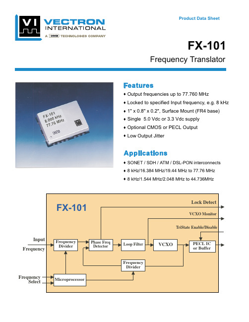
Product Data SheetFX-101Frequency TranslatorOutput frequencies up to 77.760 MHzLocked to specified Input frequency, e.g. 8 kHz 1" x 0.8" x 0.2", Surface Mount (FR4 base)Single 5.0 Vdc or 3.3 Vdc supply Optional CMOS or PECL Output Low Output JitterSONET / SDH / ATM / DSL-PON interconnects 8 kHz/16.384 MHz/19.44 MHz to 77.76 MHz8 kHz/1.544 MHz/2.048 MHz to 44.736MHzVectron's FX-101 is a crystal based frequency translator which is used to translate any input frequency such as 8 kHz, 1.544 MHz, 2.048 MHz, 19.440 MHz etc. to any specific frequency less than or equal to 77.76 MHz. The input frequency does not have to be a 50/50% duty cycle and as an example can be an 8 kHz signal with a logic high "on time" of only 1us, such as a BITS clock. The FX-101 also has the ability to translate up to any of 4 different input frequencies to one common output frequency, such as input frequencies of 8 kHz and 1.544 MHz and 19.44 MHz and any other frequency between 333 Hz and 77.76 MHz translating them to an output frequency up to 77.76 MHz.The "Input Frequency tracking capability" is the total amount of input frequency deviation in which the FX-101 is guaranteed to track or translate. As an example, a typical input clock would be 8 kHz ± 20 ppm. The FX-101 is guaranteed to track at least ±50 ppm of error over temperature/ aging/ power supply and is more than twice what most applications require. The PLL control voltage is brought out through a 470K ohm resistor. This would allow for the use of external circuitry (analog comparators or an A/D converter plus a processor) to detect when the control voltage is getting close to the limits of the pull range.(1.00)@ 140ºC to 160ºC @ >183ºCT e m p e r a t u r e ( ºC)NOTE: This FX-101 should not be subjected to a wash process that will immerse it in solvents.NO CLEAN is the recommended procedure.All components outside the dotted line box are user supplied components and/or connections. This is just one possible configuration of the FX-101. For additional information about your specific needs please contact our Factory.Although protection circuitry has been designed into this device, proper precautions should be taken to avoid exposure to electrostatic discharge (ESD) during handling and mounting. VI employs a human-body model (HBM) and a charged-device model (CDM) for ESD-susceptibility testing and protection design evaluation. ESD voltage thresholds are dependent on the circuitparameters used to define the mode.Although no industry-wide standard has been adopted for the CDM, a standard HBM (resistance = 1500 ohms, capacitance =100pf) is widely used and therefore can be used for comparison purposes. The HBM ESD threshold presented here was obtained by using these circuit parameters.ESD Threshold VoltageModelThreshold Unit Human-Body (HBM)Charged-Device500500V min V min。
RTC6701-DST-004
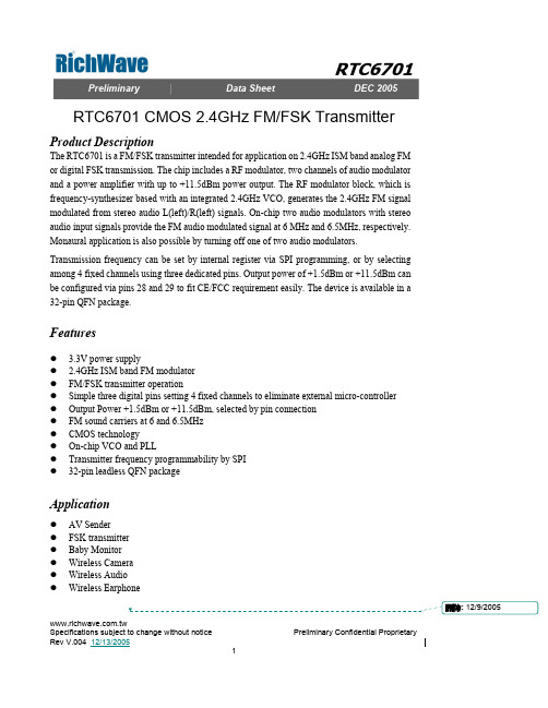
PreliminaryData SheetDEC 2005Specifications subject to change without notice Preliminary Confidential ProprietaryRTC6701 CMOS 2.4GHz FM/FSK TransmitterProduct DescriptionThe RTC6701 is a FM/FSK transmitter intended for application on 2.4GHz ISM band analog FM or digital FSK transmission. The chip includes a RF modulator, two channels of audio modulator and a power amplifier with up to +11.5dBm power output. The RF modulator block, which is frequency-synthesizer based with an integrated 2.4GHz VCO, generates the 2.4GHz FM signal modulated from stereo audio L(left)/R(left) signals. On-chip two audio modulators with stereo audio input signals provide the FM audio modulated signal at 6 MHz and 6.5MHz, respectively. Monaural application is also possible by turning off one of two audio modulators.Transmission frequency can be set by internal register via SPI programming, or by selecting among 4 fixed channels using three dedicated pins. Output power of +1.5dBm or +11.5dBm can be configured via pins 28 and 29 to fit CE/FCC requirement easily. The device is available in a 32-pin QFN package.Features3.3V power supply2.4GHz ISM band FM modulator FM/FSK transmitter operationSimple three digital pins setting 4 fixed channels to eliminate external micro-controller Output Power +1.5dBm or +11.5dBm, selected by pin connection FM sound carriers at 6 and 6.5MHz CMOS technology On-chip VCO and PLLTransmitter frequency programmability by SPI 32-pin leadless QFN packageApplicationAV Sender FSK transmitter Baby Monitor Wireless Camera Wireless AudioWireless EarphonePreliminaryData SheetDEC 2005Specifications subject to change without notice Preliminary Confidential ProprietaryBlock DiagramPreliminaryData SheetDEC 2005Specifications subject to change without notice Preliminary Confidential ProprietaryPIN DescriptionsPIN NAME I/O FUNCTION 1 VCOVDD Supply IN VDD for VCO 1 2 VT Analog IN Vtune for VCO 3 GND Analog GND Analog GND4 CP Analog OUT Synthesizer charge pump output5 AVT2 Analog IN Vtune for audio 2 PLL6 ACP2 Analog OUT Charge pump for audio 27 AOUT2 Analog OUT FM modulated audio 2 output8 AVDD2 Supply IN 3.3V power supply for audio 2 modulator 9 AOUT1 Analog OUTFM modulated audio 1 output 10 NC NC Not connected11 AVT1 Analog IN Vtune for audio1 PLL 12 ACP1 Analog OUT Charge pump for audio 113 AVDD1 Supply IN 3.3V power supply for audio 1 modulator 14 VDD Supply IN 3.3V Digital DC power supply 15 SPI_SE Digital IN Switch mode or SPI selection16 BCR Analog I/O Reference current by connecting 10k resistor 17 REG1D8 Analog OUT Regulator OUT 1.8V regulator output 18 PD_REG1D8 Digital IN Power down for 1.8V regulator 1: Power Down; 0: Power On 19 XTAL1 Analog I/O Crystal connection 20 XTAL2 Analog I/O Crystal connection21 VDD33 Supply IN 3.3V DC power supply for digital circuits CS0 Digital IN Easy channel selection 2 22 SPICLK Digital IN SPI digital controlCS1 Digital IN Easy Channel selection 2 23 SPILE Digital IN SPI digital controlCS2Digital IN Easy Channel selection 2 24 SPIDATA Digital IN SPI digital control25 BXDigital IN Alternative band selection 2 26 SYNVSS Digital GND Digital GND for synthesizer 27 RFGND2 Analog GND RF GND28 PAOUT2 Analog OUT Connect with PAOUT1 for +12dBm output 29 PAOUT1 Analog OUT PA output for 0dBm 30 RFGND1 Analog GND RF GND31 PAVDD Supply IN3.3V VDD for PA ESD 32NCNot connectedNote 1. Connect to 3.3V supply through a resistor. Nominal voltage at this pin=2.5V.Note 2. Digital pins (22, 23, 24, 25) with internal pull-high circuits can be left floating for logical high.PreliminaryData SheetDEC 2005ELECTRICAL SPECIFICATIONS(1) Absolute Maximum RatingsSYMBOL PARAMETERRatings UNIT Tstr Storage Temperature Range -65 to +150 °C Totr Operating Temperature Range -40 to +85 °C Vdd Supply Voltage -0.5 to +5 V VlogLogic control signal-0.5 to +5VThe maximum rating must not be exceeded at any time. Do not operate the device under conditions outside the above ratings.(2) DC Electrical CharacteristicsSYMBOL PARAMETERCONDITION MIN. TYP. MAX. UNI T Tj Temperature Range - -40 25 85 °C VDD Supply Voltage3.1 3.3 3.5 V I_RF Power consumption for chip (+12dBm output)TT 25C, 3.3V 49 mA I_module Power consumption for module TT 25C, 3.3V 54 mA I_pd Power down current leakage TT 25C, 3.3V 1 10 uA Fref Oscillator operating frequency8MHz V_IH High Level Input Voltage for digital interfaceV_IO=3V0.7xV_IO V_IO+0.3 V V_ILLow Level Input Voltage for digital interface-0.30.3xV_IOVPreliminaryData SheetDEC 2005Specifications subject to change without notice Preliminary Confidential Proprietarywith the fundamental signal at low power modedesign* All with proper match at the PA output, before further ceramic filtering.VideoZin_video Video input impedance (as reference design)75 Ω Vin_video Video peak to peak input voltage (as reference design) 75 ohm load 1 Vpp AudioVTAA Video carrier to audio carrier ratio (as reference design) No video and audiosignal in 24 27 30 dBc fau Audio carrier frequency Left sound Right sound 6 6.5 MHz Vin_audioAudio peak to peak voltage at audio Vtune pin@1KHz tone input with ±45KHz frequency deviation30mVppTHD Total harmonic distortion measurement by RTC6711 receiver@1KHz tone input with ±45KHz frequency deviation0.46 0.9 %F_corner 3dB corner frequency of pre-emphasis (as reference design)4 kHzSNR_AAudio SNR (as reference design,) With pre-emphasis/ de-emphasis,@1KHz tone input with ±45KHz frequency deviation45 47.5 dBPreliminaryData SheetDEC 2005Specifications subject to change without notice Preliminary Confidential ProprietaryNote:1.) On the rising edge of the clock, one bit of data is transferred into the shirt register.2.) LE should be *L* when the data is transferred into the shirt register.PreliminaryData SheetDEC 2005Specifications subject to change without notice Preliminary Confidential ProprietaryChannel SelectionThere are two principle modes for channel selection.(1) Easy channel selection modeWhen pin 15 (SPI_SE) is set at low (0V), the chip operates in easy channel selection mode. Operation frequency can be selected by the pins 25(BX), 24(CS2), 23(CS1) and 22(CS0). The selected channel frequencies are listed in the table below. BX=0Pin25 (BX) is pulled to low for normal ISM band, and operation frequency table show as following Table.Pin22/Pin23/Pin24 CS0/CS1/CS2 BX SPI_SE011101 110 111 02414MHz2432MHz2450MHz2468MHzBX=1Reserved for alternative band selection(2) SPI modeWhen pin 15 (SPI_SE) is set at high (3.3V), the chip works as in the SPI mode and the pins 24(SPIDATA), 23(SPILE) and 22(SPICLK)are used for ‘SPI’ inputs for 3-wire programming interface.SPI REGISTER DEFINITIONAddress 00: Synthesizer Register ABits 23 22 21 20 19 18 17 16 15 14 13 12 11 10 9 8 7 6 5 4 3 2 1 0 Name Syn_RF_R_Reg Syn_RF_A_Reg addressPIN R14 R13 R12 R11 R10 R9 R8 R7 R6 R5 R4 R3 R2 R1 R0 A6 A5 A4 A3 A2 A1 A0Default 0 0 0 0 0 0 1 1 0 0 1 0 0 0 0 0 1 1 1 1 0 0 0 0Syn_RF_R_Reg : R counter divider ratio control register [14:0] Syn_RF_A_Reg : A counter divider ratio control register [6:0] R14=MSB, R0=LSBFor integer N Synthesizer, the RF LO frequency is calculated by (N*64+A)*f ref /R, where f ref is the frequency of external reference oscillator (8 MHz). Ex for channel 1 operation (f = 2414MHz) Default: R=400; N=1885; A=602414MHz=(1885*64+60)*8MHz/400SPI_SE (Pin 15) Mode High SPI mode Low Easy channel selection modePreliminaryData SheetDEC 2005Specifications subject to change without notice Preliminary Confidential ProprietaryAddress 01: Synthesizer Register BBits 23 22 21 20 19 18 17 16 15 14 13 12 11 10 987 654 3 21NameSyn_RF_N_RegCP_RFSC _trlNot usedaddress PIN N12 N11 N10 N9 N8 N7 N6 N5 N4 N3 N2 N1 N0Default 0 0 1 1 1 0 1 0 1 1 1 0 1 0 0 1 0 X X X XX 0 1Syn_RF_N_Reg : N counter divider ratio control register [12:0] (default R ratio=400) CP_RF [2:0] RF charge pump current control (from 50uA to 6mA, default=100uA)SC_ctrl: external/internal SC_select control pin (LOW=internal). If set “1” in RTC67 series then charge pump will enter the testing mode ----Only for internal testingAddress 10: Synthesizer Register CBits 23 22 21 20 19 18 17 16 15 14 13 12 11 10 9 8 7 6 5 4 3 2 1 0Name Not Used Not Used Mout PRE_control Not usedPA_Bias address PIN 8 7 6 5 4 3 2 1 0 1 0 2 1 0 1 0 Default X X X X X X X X X X X X 0 0 1 0 1 X X X 1 0 1 0Mout : Multi-function output select(00,01,11,10)=(gnd, lock in detect ,RF divider output, reference clk output) PRE_control[2:0]: prescalar current control (20~140u) PA_Bias[1:0]: PA bias resistor selectionAddress 11: Synthesizer Register DBits 23 22 21 20 19 18 17 16 15 14 13 12 11 10 98 7 6 54 3 2 1 0 Name Not UsedVCOSC PA_PD Audio_div Notuse dACP address PIN1 0 7 6 5 4 32 1 0 DefaultXXXXXXXXXXX111 0 0 0 1 1VCOSC[1:0]: 2-bit RF VCO switch capacitor control in RTC6701PA_PD 1: PA power down control, 0 for power on and 1 for power downAudio_div[5:0]: Reference clock division ratio in audio carrier frequency synthesizer.ACP[1:0]: Audio charge pump current control (default 00:20uA, 01:50uA, 10: 110uA, 11: 140uA)Preliminary Data Sheet DEC 2005PACKAGEQFN 5X5 32 pinsSpecifications subject to change without notice Preliminary Confidential Proprietary。
HFBR-2412中文资料
Fiber-Optic Transmitter and ReceiverReliability Data IntroductionAgilent Technologies’ quality system includes an ongoing reliability monitor program to generate a data base from which this reliability data sheet is published.Transmitter Reliability The HFBR-0400 Series fiberoptic transmitters incorporate AlGaAs emitters and double lens optical systems. This design allows the HFBR-14XX transmitters to be driven at a relatively low current level for a specified amount of coupled power into the fiber. Because transmitter forward currents are proportional to failure rates, a low current translates into excellent transmitter reliability. To further improve reliability, Agilent has implemented a proprietary wafer screening technology that identifies dislocations whichcan lead to the formation of darkline defects (the primary mechanism for transmitter light output failures).HFBR-0400 SeriesTransmitters:HFBR-1402, -1412, -1404, -1414Receivers:HFBR-2402, -2412, -2406, -2416 Transmtter reliability data hasbeen calculated using 100 mAforward current and a 100% dutyfactor. In many actual useconditions, a 50% duty factor andlower forward currents are highlyprobable. When this is true,transmitter reliability will besubstantially better. The degree ofimprovement can be projected byexamining the footnotes below theHFBR-14XX data.Reliability PredictionModelThe reliability prediction modelused to project failure rate andmean time to failure (MTTF) atvarious temperatures shown in thesecond table assumes anexponential cumulative failurefunction (constant failure rate).The Arrhenius temperaturederating equation is used. AgilentTechnologies assumes no failuremechanism change between stressand use conditions. A conservativeactivation energy of 0.43 eV wasused and is derived from MIL-HDBD-217 for hybrid devices.Confidence intervals are basedupon the chi-squaredprediction method associated withexponential distributions.Fiber-Optic TransmitterReliability Data HFBR-1402HFBR-1412HFBR-1404HFBR-1414High Temperature Operating Life TestA. Demonstrated PerformanceTest Equivalent Test Condition Samples Device Hours Failures HTOL T A = 85°C, I F = 100 mA880 units879,5003B. Failure CriteriaFailure has occurred when the unitfails catastrophically, or when thelight output power decreases 3 dB.Point Typical PerformancePerformance [1]in Time [2]in Time(90% Confidence) Ambient Junction MTTF [1]FITs [3]MTTF [2]FITs [3] Temperature (°C)Temperature (°C)(hours)(/109 Hours)(hours)(/109 Hours) 85100293,0003411131,00075968095352,0002844158,00063347590424,0002360190,00052557085514,0001947231,00043376580626,0001598281,00035606075766,0001305344,00029055570945,0001059424,000235750651,172,000854526,000190145601,462,000684657,000152340551,838,000544825,000121235502,326,0004301,044,00095830452,965,0003371,331,00075125403,810,0002631,711,000585C. Failure Rate Prediction for Random Failures (I F @ 100 mA, 100% duty cycle)Notes:1. The point MTTF (representing an esti-mate of the mean point MTTF) is the total device hours divided by either the number performance that is expected from 90% ofall samples. This confidence interval isbased on the statistics of the distribution offailure rates prior to the onset of wear out.Refer to MIL-STD-690 for details of thismethodology.Fiber-Optic Link ReceiverReliability DataHFBR-2402HFBR-2412High Temperature Operating Life TestA. Demonstrated PerformanceTest Equivalent Test Condition Samples Device Hours Failures HTOL T A = 85°C, V CC = 5.25 V3,9602,370,0001B. Failure CriteriaFailure has occurred when the unitfails catastrophically. One devicefailed to switch logic states.Point Typical PerformancePerformance [1]in Time [2]in Time(90% Confidence) Ambient Junction MTTF [1]FITs [3]MTTF [2]FITs [3] Temperature (°C)Temperature (°C)(hours)(/109 Hours)(hours)(/109 Hours) 851002,370,000421609,0001,64080952,880,000346742,0001,34075903,530,000282909,0001,09070854,350,0002291,120,00089265805,400,0001841,390,00071960756,740,0001481,730,00057655708,480,0001172,180,000458506510,700,000932,750,000362456013,600,000733,510,000284405517,500,000564,520,000221355022,700,000435,850,000170304529,700,000337,650,000130254039,200,0002510,000,00099C. Failure Rate Prediction, Receiver (V CC = 5.25 V)Notes:1. The point MTTF (representing an esti-mate of the mean point MTTF) is the total device hours divided by either the number performance that is expected from 90% ofall samples. This confidence interval isuseful life failures. Refer to MIL-STD-690 fordetails of this methodology.Fiber-Optic Link ReceiverReliability DataHFBR-2406HFBR-2416High Temperature Operating Life TestA. Demonstrated PerformanceTest Equivalent Test Condition Samples Device Hours Failures HTOL T A = 85°C, V CC = 5.25 V2,2502,250,0000B. Failure CriteriaFailure has occurred when the unitfails catastrophically.Point Typical PerformancePerformance [1]in Time [2]in Time(90% Confidence) Ambient Junction MTTF [1]FITs [3]MTTF [2]FITs [3] Temperature (°C)Temperature (°C)(hours)(/109 Hours)(hours)(/109 Hours) 851002,250,000444977,164102380952,698,5163711,171,95385375903,252,6873071,412,62770870853,941,1732541,711,63358465804,801,4322082,085,24048060755,882,7441702,554,84939155707,250,3821383,148,80831850658,991,4071113,904,927256456011,222,799894,874,010205405514,102,949716,124,846163355017,848,023567,751,315129304522,755,516449,882,616101254029,238,4093412,698,10779C. Failure Rate Prediction, Receiver (V CC = 5.25 V)Notes:1. The point MTTF (representing an esti-mate of the mean point MTTF) is the total device hours divided by either the number performance that is expected from 90% ofall samples. This confidence interval isuseful life failures. Refer to MIL-STD-690 fordetails of this methodology.HFBR-0400 Mechanical and Environmental Test Data [1]MIL-STD-883D Units Total Test Name Reference Test Conditions Tested Failed Temperature Cycle1010500 cycles from -55 to +125°C, 15 minutes20201at extremes, 5 minutes transfer. [1]HFBR-1414500 cycles from -55 to +125°C, 15 minutes20900at extremes, 5 minutes transfer.[1]HFBR-2416 85/85T A = 85°C, 85% relative humidity,21407No bias, duration = 1,000 hours. [1]HFBR-1414T A = 85°C, 85% relative humidity,22206V CC = 5 volts, Duration = 1,000 hours[1]HFBR-2416 High Temperature1008T A = 125°C800 Storage Condition B1000 hoursResistance to2015Three 1 minute immersions.200 Solvents Brush after solvent immersion.Chemical Resistance— 5 minutes in Acetone, Methanol, Freon TF200and Boiling WaterVibration Variable 2007,20 G min., 20 to 2000 Hz.200 Frequency Condition B4, 4 minute cycles each X, Y, and Z.Thermal Shock1011-55°C to +125°C, 15 cycles600Condition B 5 min. dwell / 10 sec. transferMechanical Shock2002, 5 blows each X1, X2, Y1, Y2, Z1, Z2600Condition B1500 G, 0.5 msec. pulse.Port Wear Test [2]T A = 25°C500 connectorings200Less than 1 dBm variationConnector Side T A = 25°C 1 kg side load100 Load [3]Less than 1 dBm variationPort Strength [4]T A = 25°C 6 kg-cm (5.21 inch-lbs), no port damage100 Seal-Dye Penetrant101445 psi, 10 hours200 (Zyglo)Condition D No Leakage into microelectronic cavitySolderability2003245°C300 ESD Method 3015Human body model @ 10,000 V50HFBR-1414Human body model @ 2,000 V50HFBR-2402Human body model @ 1000 V50HFBR-2416Notes: See following page.Notes:1. Devices were preconditioned with 10 second, 260°C solder dip and 20 cycles, -40°C to 85°C, temperature cycle.2. Coupled power measurements were maximized before and after stress in determining the 1 dBm variation for SMA HFBR-0400 products. HFBR-0400 ST products do not require this due to the improved coupling design.3. The Connector Side Load test was only applied to HFBR-0400 SMA products. The Connector Side Load testing required that the housing be held so to prevent the leads from yielding. The load was applied through a SMA connectored fiber optic cable, perpendicular to the port. The product family is designed to limit cable and ferrule damage due to cable loading. The support and active leads should yield before damage to the cable or connector occurs. If extreme mechanical abuse of the cable/ connector is anticipated please contact Agilent’s Application Department for suggestions about mechanical strain relief. Due to the spring loaded feature of the ST connector, HFBR-0400 ST products will experience 1 dBm coupled power variation at a side load of less than 1 kg.4. The Port Strength test was designed to gauge the concerns with hand tightening the connector to the fiber optic port. The limit is set to alevel beyond most reasonable hand fastening loading.5. Package tests are defined as stresses that indicate the environmental strength of the package. Units tested indicate the total number of devices taken from the product family. While not all part numbers have been subjected to each stress, worst case products have been included.。
圆贴片微带天线的辐射模式研究
摘要摘要随着时代的发展,社会的进步,人们对无线通信的需求也越来越高,一个高效率、高质量的通信系统就显得尤为的重要。
天线主要用来接收和发射电磁波,其性能的好坏对整个通信系统的通信质量影响很大。
微带天线由于其低剖面结构及易于实现圆极化工作,被广泛的应用于移动卫星通信、卫星导航、射频识别等领域。
本文在此背景之下,重点对圆形和圆环形微带天线的辐射模式进行了分析和研究。
并根据实际需求,结合这些理论和分析方法,设计了一款圆形微带天线和两款圆环形微带天线。
详细情况如下:1.基于圆贴片微带天线的主模TM11模设计了一款双频圆极化微带天线,最大辐射方向为天线法线方向。
天线采用层叠的方式实现双频工作,下层微带天线工作在低频状态,上层微带天线工作在高频状态,下层微带天线的辐射贴片作为上层微带天线的接地板。
该天线有两个端口,当对不同的端口进行激励时,天线分别工作在不同的频段。
该天线利用两个一分二馈电网络分别实现不同频率的圆极化特性,馈电网络和下层微带天线共地置于整个天线的最下方。
2.基于圆环形贴片微带天线的主模TM11模设计了一款圆极化微带天线。
圆极化微带天线采用单点馈电,通过T型功分器实现圆极化特性。
馈电网络位于圆环形贴片的内部,减少了对空间的占用,有效的减小了天线的尺寸。
天线正上方一定距离处加载寄生贴片用于展宽天线的带宽。
3.基于圆环形贴片微带天线的主模TM11模和高次模TM21模设计了一款宽带圆极化微带天线。
该天线是一个双端口天线,不同端口能分别激励起圆环形天线的TM11模与TM21模,其中TM11模式对应宽波束轴向辐射方向图,TM21模式对应全向锥形方向图。
天线处于不同工作模式时均有相应的寄生贴片起展宽带宽的作用。
以上三款天线均已加工并测试,测试结果与仿真结果相吻合,其中第一款天线和第二款天线已用于卫星导航中。
关键词:TM11模, TM21模, 双频圆极化微带天线, 双模圆极化微带天线ABSTRACTABSTRACTWith the development of the times and the progress of the society, the demand for wireless communication is becoming higher and higher. A high efficient and high quality communication system is particularly important.Antenna is mainly used to receive and transmit electromagnetic waves, and its performance has great influence on the communication quality of the entire communication system. The microstrip antenna is widely used in mobile satellite communication, satellite navigation, radio frequency identification and other fields due to its low profile structure and easy to realize circular polarization. In this context, the radiation modes of circular and circular microstrip antennas are analyzed and studied in this paper. According to the actual demand, a circular microstrip antenna and two ring microstrip antennas are designed according to these theories and analysis methods. Details are as follows:1. A dual-frequency circular polarization microstrip antenna is designed based on the main mode TM11model of the circular patch microstrip antenna, the maximum radiation direction is the normal direction of the antenna. The antenna use the cascade mode to realize the dual frequency, lower antenna working at low frequency, upper antenna working at high frequency, the radiation patch of the lower microstrip antenna as the ground floor of the upper microstrip antenna. The antenna has two ports, and works in different frequency bands when the different ports are energized. The antenna uses two separate feed networks to realize the circular polarization characteristics of different frequencies. The feed network common ground with the lower microstrip antenna, and locate at the bottom of the whole antenna.2.A circular polarization microstrip antenna is designed based on the main die TM11 module of the circular ring patch microstrip antenna. The circular polarization microstrip antenna adopts the single point feed, and the circular polarization characteristics are realized through the T type power divider. The feed network is located inside the ring patch, reducing the space occupation and effectively reducing the antenna size. A parasitic patch is loaded at a distance above the antenna to extend the bandwidth of the antenna.西安电子科技大学硕士学位论文TM11 module and the high model TM21 model of circular ring patch microstrip antenna. The antenna is a dual port antenna. Different ports of this antenna can excite different modes of the circular loops. The broad beam can be achieved with the TM11 mode excited and the conical beam can be achieved with the TM21mode excited. The circular loops working in both TM11 and TM21 modes have parasitic patches to broaden the impedance bandwidths.All three antennas have been processed and tested. The test results are in accordance with the simulation results. The first antenna and the second antenna have been used in satellite navigation.Keywords: TM11mode,TM21mode,Dual frequency circular polarization microstrip antenna,Dual mode circularly polarized microstrip antenna.插图索引插图索引图2.1 不同极化的平面波电场矢量运动示意图 (5)图2.2 空间坐标系示意图 (10)图2.3 天线馈电模型示意图 (12)图2.4 Yee单元模型示意图 (17)图2.5 四面体离散单元结构 (18)图3.1 圆形贴片天线示意图 (21)图3.2 圆形贴片不同模式的场分布(a)TM01(b)TM11(c)TM21(d)TM31 (27)图3.3 几种模式对应的馈电点 (28)图3.4 天线模型图 (29)图3.5 天线电压驻波图 (29)图3.6 天线远区场方向图 (30)图3.7 天线贴片上电流分布图 (30)图3.8 天线模型图 (31)图3.9 天线电压驻波图 (31)图3.10 天线远区场方向图 (32)图3.11 天线贴片上电流分布图 (32)图3.12 圆形贴片天线加载短路金属柱示意图 (33)图 3.13 圆形贴片天线加载短路金属柱不同模式对应电场矢量分布示意图(a)TM01(b)TM02 (34)图3.14 圆形贴片加载短路金属住数目N=1时示意图 (34)图3.15 圆环形贴片天线示意图 (35)图3.16 圆环形贴片不同模式的场分布(a)TM11(b)TM21 (37)图4.1 天线结构图 (39)图4.2 馈电网络视图 (40)图4.3 天线实物图 (41)图4.4 天线仿真与测试|S11|对比结果(a)低频,(b)高频 (41)图4.5 天线在1.616GHz和2.27GHz时的贴片电流分布图 (42)图4.6 1.616GHz处天线的仿真与测试方向图(a)xoz面,(b)yoz面 (42)图4.7 2.492GHz处天线的仿真与测试方向图(a)xoz面,(b)yoz面 (42)图4.8 天线在1.616GHz(a)和2.492GHz(b)处的仿真与测试轴比结果对比图 (43)西安电子科技大学硕士学位论文图4.10 天线实物图 (45)图4.11 天线仿真与测试|S11|对比结果 (45)图4.12 天线仿真与测试方向图(a)xoz面,(b)yoz面 (46)图4.13 天线轴比随频率变化的曲线 (46)图4.14 天线模型的示意图(a)侧视图(b)中间介质板(c)底层介质板 (47)图4.15 圆环形贴片天线输入阻抗随内外径比(a/b)的变化曲线 (49)图4.16 天线表面电流分布(a)TM11(b)TM21 (49)图4.17 天线实物照片(a)每层实物(b)组合实物 (50)图4.18 天线仿真与测试|S11|(a),|S22|(b),|S21|(c)对比结果 (50)图4.19 天线在2端口激励时仿真与测试方向图(a)xoz面,(b)yoz面 (51)图4.20 天线在2端口激励时仿真与测试轴比(a)xoz面,(b)yoz面 (51)图4.21 天线在1端口激励时仿真与测试方向图(a)xoz面,(b)yoz面 (52)图4.22 天线在1端口激励时仿真与测试轴比(a)xoz面,(b)yoz面 (52)图4.23 天线在2端口激励时不同寄生贴片高度h2对应天线|S22|(a)与轴比(b)曲线 (53)图4.24 天线在1端口激励时不同寄生贴片高度h1对应天线|S11|(a)与轴比(b)曲线 (53)图4.25 天线在2端口激励时不同寄生贴片半径R p对应天线|S22|(a)与轴比(b)曲线 (54)图4.26 天线在1端口激励时不同寄生贴片半径R sub1对应天线|S11|(a)与轴比(b)曲线 (54)图4.27 天线在2端口激励时不同环形贴片外径a1对应天线|S22|(a)与轴比(b)曲线 (54)图4.28 天线在1端口激励时不同环形贴片外径a2对应天线|S11|(a)与轴比(b)曲线 (55)表格索引J ka 的根 (26)表3.1'()0m表4.1TM11模圆极化圆环形微带天线参数 (45)表4.2宽带环形微带天线参数 (48)符号对照表符号符号名称 E 电场强度 H磁场强度 λ波长 η波阻抗 k 传输常数 Z in 输入阻抗 R in 输入电阻 X in 输入电抗 Γ 反射系数 B 绝对带宽 Br 相对带宽 U 辐射强度 P 功率 D方向性系数 A η天线效率 G 天线的增益 λg介质中的波长 J电流密度c自由空间电磁波传播速度 f频率 ε 介电常数 μ 磁导率缩略语对照表缩略语英文全称中文对照VSWR V oltage Standing Wave Ratio 电压驻波比LP Linearly Polarized 线极化CP Circularly Polarized 圆极化AR Axial Ratio 轴比LHCP Left Hand Circularly Polarized 左旋圆极化RHCP Right Hand Circularly Polarized 右旋圆极化目录目录摘要 (I)ABSTRACT (III)插图索引 (V)表格索引 ............................................................................................................................ V II 符号对照表 . (IX)缩略语对照表 (XI)第一章绪论 (1)1.1研究背景及意义 (1)1.2国内外研究现状 (2)1.3论文研究内容与结构安排 (3)第二章基本理论 (5)2.1天线的基本特征 (5)2.1.1天线的极化特性 (5)2.1.2天线的辐射方向图 (10)2.1.3天线的基本参数 (12)2.2天线的分析方法 (15)2.3本章小结 (20)第三章圆形微带天线不同模式的分析研究 (21)3.1圆形微带天线的工作模式 (21)3.1.1圆形微带天线的工作原理 (21)3.1.2圆形微带天线TM11模和TM21模分析研究 (29)3.1.3圆形微带天线TM01模和TM02模分析研究 (32)3.2圆环形微带天线的工作模式 (35)3.3本章小结 (37)第四章基于不同模式的全向天线 (39)4.1双频圆极化微带天线设计 (39)4.1.1天线设计 (39)4.1.2天线的仿真与测试结果 (41)4.2TM11模圆极化圆环形微带天线的设计 (43)4.2.1天线设计 (43)西安电子科技大学硕士学位论文4.3基于TM11模式与TM21模式的宽带环形天线 (46)4.3.1天线设计 (47)4.3.2天线的仿真与测试结果分析 (49)4.3.3天线的参数分析 (52)4.4本章小结 (55)第五章总结与展望 (57)参考文献 (59)致谢 (61)作者简介 (63)第一章绪论第一章绪论1.1研究背景及意义伴随着社会的的不断进步和发展,电子技术已经逐步走入人们的日常生活当中,这也促使电子技术进入了一个快速发展的时期,在这期间,频谱资源正在成为人类最大的可重复使用的自然资源。
RTC6701.pdf
Rev. Date From DescriptionV.002 V.00310/3/200510/31/2005R2200R2200OriginalModify the following items:1. Add pin 17 PD_REG1D8 description; 1 for power down and 0 forpower on2. Add Absolute Maximum RatingsV.004 V.004 12/1/200512/2/2005R2200R2100R22001. A dd “SPI Digital Timing Diagram” and revised date code.2. U pdate output power data.3. R emoved RX IF input in Absolute Maximum Ratings.4. A dd mini. Audio SNR.Applicant:R2200 Approvals: Document Title: Data SheetofRTC6701R2000: S.C. Wong R2500: C.J. Chao Document No.: RTC6701-DST-004R2100: J.Y. Tsai Marketing: Jack Chang R2200: W.K. DengR2300: T.S. Liou☆ Signature on file in DC ☆Contents: 8 Attach: 0Total Page: 9File Format: WordRTC6701 CMOS 2.4GHz FM/FSK Transmitter Product DescriptionThe RTC6701 is a FM/FSK transmitter intended for application on 2.4GHz ISM band analog FM or digital FSK transmission. The chip includes a RF modulator, two channels of audio modulator and a power amplifier with up to +11.5dBm power output. The RF modulator block, which is frequency-synthesizer based with an integrated 2.4GHz VCO, generates the 2.4GHz FM signal modulated from stereo audio L(left)/R(left) signals. On-chip two audio modulators with stereo audio input signals provide the FM audio modulated signal at 6 MHz and 6.5MHz, respectively. Monaural application is also possible by turning off one of two audio modulators.Transmission frequency can be set by internal register via SPI programming, or by selecting among 4 fixed channels using three dedicated pins. Output power of +1.5dBm or +11.5dBm can be configured via pins 28 and 29 to fit CE/FCC requirement easily. The device is available in a 32-pin QFN package.Features3.3V power supply2.4GHz ISM band FM modulatorFM/FSK transmitter operationSimple three digital pins setting 4 fixed channels to eliminate external micro-controllerOutput Power +1.5dBm or +11.5dBm, selected by pin connectionFM sound carriers at 6 and 6.5MHzCMOS technologyOn-chip VCO and PLLTransmitter frequency programmability by SPI32-pin leadless QFN packageApplicationAV SenderFSK transmitterBaby MonitorWireless CameraWireless AudioWireless EarphoneBlock DiagramPin DescriptionsPIN NAME I/O FUNCTION1 VCOVDD Supply In VDD for VCO12 VT Analog In Vtune for VCO3 GND Analog GND Analog GND4 CP Analog Out Synthesizer charge pump output5 AVT2 Analog In Vtune for audio 2 PLL6 ACP2 Analog Out Charge pump for audio 27 AOUT2 Analog Out FM modulated audio 2 output8 AVDD2 Supply In 3.3V power supply for audio 2 modulator9 AOUT1 Analog Out FM modulated audio 1 output10 NC NC NC11 AVT1 Analog In Vtune for audio1 PLL12 ACP1 Analog Out Charge pump for audio 113 AVDD1 Supply In 3.3V power supply for audio 1 modulator14 VDD Supply In 3.3V Digital DC power supply15 SPI_SE Digital In Switch mode or SPI selection (Internal pull high)16 BCR Analog I/O Reference current by connecting 10k resistor17 REG1D8 Analog Out Regulator OUT 1.8V regulator output18 PD_REG1D8 Digital In Power down for 1.8V regulator 1: Power Down; 0: Power On19 XTAL1 Analog I/O Crystal connection20 XTAL2 Analog I/O Crystal connection21 VDD33 Supply In 3.3V DC power supply for digital circuitsCS0 Digital In Easy channel selection2 (Internal pull high)22SPICLK Digital In SPI bus clock inputCS1 Digital In Easy Channel selection2(Internal pull high)23SPILE Digital In SPI bus latch enable inputCS2 Digital In Easy Channel selection2 (Internal pull high)24SPIDATA Digital In SPI bus data input25 BX Digital In Alternative band selection2 (Internal pull high)26 SYNVSS Digital GND Digital GND for synthesizer27 RFGND2 Analog GND RF GND28 PAOUT2 Analog Out Connect with PAOUT1 for +12dBm output29 PAOUT1 Analog Out PA output for 0dBm30 RFGND1 Analog GND RF GND31 PAVDD Supply In 3.3V VDD for PA ESD32 NC NC NCNote 1. Connect to 3.3V supply through a resistor. Nominal voltage at this pin=2.5V.Note 2. Digital pins (15, 22, 23, 24, 25) with internal pull-high circuits can be left floating for logical high.ELECTRICAL SPECIFICATIONS(1) Absolute Maximum RatingsSYMBOL PARAMETER Ratings UNITTstr Storage Temperature Range -65 to +150 °CTotr Operating Temperature Range -40 to +85 °CVdd Supply Voltage -0.5 to +5 VVlog Logic control signal -0.5 to +5 VThe maximum rating must not be exceeded at any time. Do not operate the device under conditions outside the above ratings.(2)DC Electrical CharacteristicsSYMBOL PARAMETER CONDITION MIN. TYP. MAX. UNITTj Temperature Range - -40 25 85 °C VDD Supply Voltage 3.1 3.3 3.5 VI_RF Power consumption for chip(+12dBm output)TT 25C, 3.3V 49mAI_module Power consumption for module TT 25C, 3.3V 54 mA I_pd Power down current leakage TT 25C, 3.3V 1 10 uA Fref Oscillator operating frequency 8 MHzV_IH High Level Input Voltage for DigitalInterfaceV_IO=3V 0.7xV_IO V_IO+0.3VV_IL Low Level Input Voltage for DigitalInterface-0.3 0.3xV_IOV(3) Transmitter SpecificationsSYMBOL PARAMETER CONDITION MIN. TYP. MAX. UNIT Fc Frequency Range 2.37 2.51 GHzPout_H* Maximum output power at highpower modeConnect PAOUT1and PAOUT210.5 11.5 12.5 dBmPout_L* Maximum output power at lowpower modeConnect PAOUT1only0.5 1.5 2.5 dBm2ndH_H* The 2nd Harmonic referencedwith the fundamental signal athigh power modeWith referencefilter design-30dBcPN The phase noise at 2414GHz 100KHz offset1MHz offset-85-110dBc/Hz3rdH_H* The 3rd Harmonic referencedwith the fundamental signal athigh power modeWith referencefilter design-40 dBc2ndH_L* The 2nd Harmonic referencedwith the fundamental signal atlow power modeWith referencefilter design-30 dBc3rdH_L* The 3rd Harmonic referencedwith the fundamental signal atlow power modeWith referencefilter design-40 dBc* All with proper match at the PA output, before further ceramic filtering.(3) Transmitter Specifications (continued)SYMBOL PARAMETER CONDITION MIN. TYP. MAX. UNIT VideoZin_video Video input impedance (asreference design)75 ΩVin_video Video peak to peak input voltage(as reference design)75 ohm load 1 Vpp AudioVTAA Video carrier to audio carrierratio (as reference design) No video and audiosignal in24 27 30 dBcfau Audio carrier frequency Left soundRight sound66.5MHzVin_audio Audio peak to peak voltage ataudio Vtune pin @1KHz tone inputwith ±25KHzfrequency deviation30mVppTHD Total harmonic distortionmeasurement by RTC6711receiver @1KHz tone inputwith ±25KHzfrequency deviation0.6 0.9 %F_corner 3dB corner frequency ofpre-emphasis (as referencedesign)4 kHzSNR_A Audio SNR (as referencedesign,) With pre-emphasis/de-emphasis, @1KHz tone inputwith ±25KHzfrequency deviation45 47 dBNote:1.) On the rising edge of the clock, one bit of data is transferred into the shirt register.2.) LE should be *L* when the data is transferred into the shirt register.Channel SelectionThere are two principle modes for channel selection.SPI_SE (Pin 7) High LowMode SPI Mode Easy Channel Selection Mode(1) Easy channel selection modeWhen pin 15 (SPI_SE) is set at low (0V), the chip operates in easy channel selection mode. Operation frequency can be selected by the pins 25(BX), 24(CS2), 23(CS1) and 22(CS0). The selected channel frequencies are listed in the table below.BX=0Pin25 (BX) is pulled to low for normal ISM band, and operation frequency table show as following Table.Pin22/Pin23/Pin24CS0/CS1/CS2BX SPI_SE011 101 110 1110 0 2414MHz 2432MHz 2450MHz 2468MHzBX=1Reserved for alternative band selection(2) SPI modeWhen pin 15 (SPI_SE) is set at high (3.3V), the chip works as in the SPI mode and the pins 24(SPIDATA), 23(SPILE) and 22(SPICLK) are used for ‘SPI’ inputs for 3-wire programming interface. The BX is “don’t care”.SPI REGISTER DEFINITIONAddress 00: Synthesizer Register ABits 23 22 21 20 19 18 17 16 15 14 13 12 11 10 9 8 7 6 5 4 3 2 1 0Name Syn_RF_R_Reg Syn_RF_A_Reg addressPIN R14 R13 R12 R11 R10 R9 R8 R7 R6 R5 R4 R3 R2 R1 R0 A6 A5 A4 A3 A2 A1 A0Default 0 0 0 0 0 0 1 1 0 0 1 0 0 0 0 0 1 1 1 1 0 0 0 0Syn_RF_R_Reg : R counter divider ratio control register [14:0]Syn_RF_A_Reg : A counter divider ratio control register [6:0]R14=MSB, R0=LSBFor integer N Synthesizer, the RF LO frequency is calculated by (N*64+A)*f ref/R, where f ref is the frequency of external reference oscillator (8 MHz). Ex for channel 1 operation (f = 2414MHz)Default: R=400; N=1885; A=602414MHz=(1885*64+60)*8MHz/400Address 01: Synthesizer Register BBits 23 22 21 20 19 18 17 16 15 14 13 12 11 10 9 8 7 6 5 4 3 2 1 0Name Syn_RF_N_Reg CP_RF SC_trlNot usedaddressPIN N12 N11 N10 N9 N8 N7 N6 N5 N4 N3 N2 N1 N0Default 0 0 1 1 1 0 1 0 1 1 1 0 1 0 0 1 0 X X X X X 0 1 Syn_RF_N_Reg : N counter divider ratio control register [12:0] (default R ratio=400)CP_RF [2:0] RF charge pump current control (from 50uA to 6mA, default=100uA)SC_ctrl: external/internal SC_select control pin (LOW=internal). If set “1” in RTC67 series then charge pump will enter the testing mode ----Only for internal testingAddress 10: Synthesizer Register CBits 23 22 21 20 19 18 17 16 15 14 13 12 11 10 9 8 7 6 5 4 3 2 1 0Name Not Used Not Used Mout PRE_control Not used PA_Bias addressPIN 8 7 6 5 4 3 2 1 0 1 0 2 1 0 1 0Default X X X X X X X X X X X X 0 0 1 0 1 X X X 1 0 1 0 Mout : Multi-function output select(00,01,11,10)=(gnd, lock in detect ,RF divider output, reference clk output)PRE_control[2:0]: prescalar current control (20~140uA)PA_Bias[1:0]: PA bias resistor selectionAddress 11: Synthesizer Register DBits 23 22 21 20 19 18 17 16 15 14 13 12 11 10 9 8 7 6 5 4 3 2 1 0Name Not Used VCOSC PA_PD Audio_divNotusedACP addressPIN 1 0 7 6 5 4 3 2 1 0Default X X X X X X X X X X X 1 0 0 0 1 0 0 1 0 0 0 1 1 VCOSC[1:0]: 2-bit RF VCO switch capacitor control in RTC6701PA_PD 1: PA power down control, 0 for power on and 1 for power downAudio_div[5:0]: Reference clock division ratio in audio carrier frequency synthesizer.ACP[1:0]: Audio charge pump current control (default 00:20uA, 01:50uA, 10: 110uA, 11: 140uA)PACKAGE QFN 5X5 32 pins。
Wilkinson型功率分配器设计_郑强林
据设计频率范围的要求,干路阻抗变换段采用 chebyshev 低通滤波器原型结构,支路阻抗变换段 采用最大平坦度的四分之一波长阶梯阻抗变换 段,两支路之间通过隔离电阻以提高支路之间的 隔离度。其仿真模型图、实物图及仿真曲线测试 曲线如下图 4~7 所示。
上式中,各尺寸突变处的反射系数或其相对 值,按所要求的某种规律取值,便可得到二项式 阻抗变换器,切比雪夫阻抗变换器等。
图 7 3dB 功分器隔离度仿真及测试结果
239
微波学报
2014 年 6 月
等, 译. 北京: 电子工业出版社, 2006. [4] 闫闰卿, 李英惠. 微波技术基础[M]. 3 版. 北京: 北京 理工大学出版社, 2004. [5] Wilkinson E J. An N-way Hybrid Power Divider[J]. IRE Trans. on Microwave Theory and Tech., 1960, 8(1): 116-118. [6] Yee H Y, Chang F C, Audeh N F. N-way TEM-mode broadband power dividers[J]. IEEE Trans. on Microwave Theory Tech., 1970, 18(10): pp682-688. [7] 何猛. 超宽带微波功分器的研制[D]. 成都: 电子科技 大学, 2009. 郑强林 男,1983 年生,硕士研究生。主要研究方向:高
这样,反映在第一个尺寸突变处的总反射系数为
1 2e j2 3e j4 ... i e j2(i1) ...n1e j2n (13)
或写成
238
微波学报
2014 年 6 月
抖动分析原理及安捷伦公司抖动分析解决方案
P3
0.980ns -0.030ns -0.020ns
(0.990/1.010/0.980/1.020)
P4
1.020ns 周期 0.040ns 周期到周期 0.000ns时间间隔误差
周期抖动 = 18.3ps RMS
周期到周期抖动 = 36.1ps RMS 时间间隔误差 = 9.6ps RMS
(0.020/-0.030/0.040)
2 1
4
Rise Fall
3
L_pkg C_comp R_pkg C_pkg
5
电路的不稳定性
PLL问题 同步开关噪声 互连阻抗不连续,互连损耗
上游的参考时钟
收发器发送的数据是以参考时钟为基准的,如果参考时钟
抖动过大。。。 使得抖动预估更困难 成为系统抖动
小结:抖动的成因
• 标准偏差 .
(所有测得的定时错误的RMS值).
• 峰 -峰值 .
(测得的定时错误的最大与最小值之差).
TIE的测量需要参考时钟.
常见的抖动术语小结
0.0ns 0.990ns 2.000ns 2.980ns 4.000ns
P1
0.990ns -0.010ns
P2
1.010ns 0.020ns 0.000ns
率噪声的方式显现出来。
目录
抖动的概念
抖动的成因 常见的抖动术语 抖动的分解 抖动测试分析方案
抖动的成因
热噪声
注入噪声
线路不稳定性 上游时钟
热噪声
随机性的 , 是多个随机抖动源的组合性现象 噪声所导致的抖动的分布是高斯与无边际的
注入噪声
确定性的, 能被确认为一些固有的成因 确定性抖动分布是有边际的,其频谱通常呈现为分离的谐波
- 1、下载文档前请自行甄别文档内容的完整性,平台不提供额外的编辑、内容补充、找答案等附加服务。
- 2、"仅部分预览"的文档,不可在线预览部分如存在完整性等问题,可反馈申请退款(可完整预览的文档不适用该条件!)。
- 3、如文档侵犯您的权益,请联系客服反馈,我们会尽快为您处理(人工客服工作时间:9:00-18:30)。
A 40-GHz Frequency Divider in 90-nm CMOS Technology
Muhammad Usama and Tad. A. Kwasniewski Department of Electronics, Carleton University 1125 Colonel By Drive, Ottawa ON, K1S 5B6 Canada. {musama, tak}@doe.carleton.ca
Abstract-This paper presents the design of a high-speed wide-band frequency divider. The divider core is formed with a low voltage swing current mode logic (CML) structure, which enables high frequency operation at very low power dissipation. The divider exhibits very wide locking range from 4GHz - 41GHz, and it has an input sensitivity of -31dBm at 30GHz. The divider core draws only 750µA from a 1.2V supply. Post layout simulation results in 90-nm CMOS technology are provided.
I. INTRODUCTION Frequency dividers are used in many communications applications such as frequency synthesizers, timing-recovery circuits, and clock generation circuits. In a phase locked loop (PLL) a frequency divider is employed within the loop to divide down the local oscillator frequency and to provide the programmability of the synthesizer. Frequency divider is one of the most critical blocks of the system because it operates at the highest frequency. In particular, the power reduction of the frequency divider in the first stage is effective in realizing a low-power PLL. This is the key point for the high-speed operation and low power consumption. The phase noise generated by the divider can affect the synthesizer noise performance within the PLL band, especially if a high division factor is used. In fact, the divider noise power is multiplied by the square of the division factor, when it is transferred to the PLL output [1]. Digital frequency dividers are the most popular divider structures in use today. They offer divider ratio programmability, higher division ratios and easier digital control. The fundamental element of a digital frequency divider is a D-type flip-flop, or two level-sensitive latches in a master-slave configuration [2]. These dividers achieve a broader bandwidth than other types of dividers in low to medium range of frequencies. High-speed digital frequency dividers are typically implemented using the current mode logic (CML) latches. The CML lathes exhibit better performance than other clocked storage elements. Large frequency ranges are not therefore uncommon in these dividers that use CML style [12]. With the aggressive scaling of CMOS transistors, multi-gigahertz dividers are now realizable in CMOS technologies. Several high-speed frequency dividers in modern
CMOS technologies have been reported in recent publications [6]-[11], [13], and [14].
This paper presents the design of a CML based frequency divider in a state-of-the-art 90-nm CMOS technology. The presented divider achieves not only a very high operating frequency but reasonably low power dissipation. The divider structure and its operation are described in Section-II. Post layout simulation results in 90-nm CMOS technology are also provider in Section-III along with a comparison of the presented divider with other recently published results.
II. DIVIDER STRUCTURE
Conventionally for a divider application, two identical CML latches are used in a master-slave configuration as shown in Fig. 1. Because of the parasitic capacitance of the transistors of sample circuit, the tail current must be sufficiently high to achieve a wider range of linearity, a higher slew rate and a larger transconductance. On the other hand the hold circuit does not need such a large bias current. These conflicting requirements can not be reconciled in conventional CML latch design because they have only a single constant current source. It is possible to simplify the usual CML latch clocking structure by employing a single clock transistor pair to switch the current between the sample and hold pair of the master and slave latches [2]. This new configuration uses a single bias
CLKCLKQRLVbiasRLIssRLVbiasRLIssQCLKCLKQQ Fig. 1. Conventional CML master-slave latch as a divider.
411-4244-0417-7/06/$20.00 ©2006 IEEEAuthorized licensed use limited to: Carleton University. Downloaded on July 17, 2009 at 13:08 from IEEE Xplore. Restrictions apply.