高速模数转换器ADC的INLDNL测量
ADC精度讲解
ADC 分辨率和精度的区别rourou 2015-9-9 下午3:10分辨率和精度这两个,经常拿在一起说,才接触的时候经常混为一谈。
对于ADC来说,这两样也是非常重要的参数,往往也决定了芯片价格,显然,我们都清楚同一个系列,16位AD一般比12位AD价格贵,但是同样是12位AD,不同厂商间又以什么参数区分性能呢?性能往往决定价格,那么什么参数对价格影响较大呢?不好意思,我其实还是有些迷惑的,但是看了下篇文章,至少知道“精度”是有很大影响力的。
该篇文章主要解释ADC分辨率和精度的区别,非常详细且易懂,值得一看,全文如下:最近做了一块板子,当然考虑到元器件的选型了,由于指标中要求精度比较高,所以对于AD的选型很慎重。
很多人对于精度和分辨率的概念不清楚,这里我做一下总结,希望大家不要混淆。
我们搞电子开发的,经常跟“精度”与“分辨率”打交道,这个问题不是三言两语能搞得清楚的,在这里只作抛砖引玉了。
简单点说,“精度”是用来描述物理量的准确程度的,而“分辨率”是用来描述刻度划分的。
从定义上看,这两个量应该是风马牛不相及的。
(是不是有朋友感到愕然^_^)。
很多卖传感器的JS就是利用这一点来糊弄人的了。
简单做个比喻:有这么一把常见的塑料尺(中学生用的那种),它的量程是10厘米,上面有100个刻度,最小能读出1毫米的有效值。
那么我们就说这把尺子的分辨率是1毫米,或者量程的1%;而它的实际精度就不得而知了(算是0.1毫米吧)。
当我们用火来烤一下它,并且把它拉长一段,然后再考察一下它。
我们不难发现,它还有有100个刻度,它的“分辨率”还是1毫米,跟原来一样!然而,您还会认为它的精度还是原来的0.1毫米么?(这个例子是引用网上的,个人觉得比喻的很形象!)回到电子技术上,我们考察一个常用的数字温度传感器:AD7416。
供应商只是大肆宣扬它有10位的AD,分辨率是1/1024。
那么,很多人就会这么欣喜:哇塞,如果测量温度0-100摄氏度,100/1024……约等于0.098摄氏度!这么高的精度,足够用了。
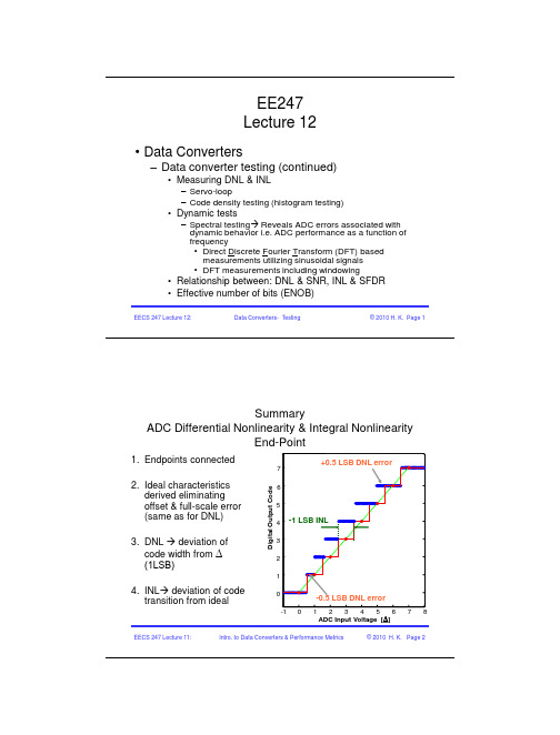
ADC中anl和dnl定义
EECS 247 Lecture 12:
Data Converters- Testing
© 2010 H. K. Page 12
Histogram Test Setup
VREF
fS
Ramp VREF ADC
0
Time
PC
• •
Slow (wrt conversion time) linear ramp applied to ADC DNL derived directly from total number of occurrences of each code @ the output of the ADC
DVM measures the average input including the glitch
time
EECS 247 Lecture 11: Intro. to Data Converters & Performance Metrics
© 2010 H. K. Page 10
Code Boundary Servo
– They can have very high resolutions (8½ decimal digit meters are inexpensive) – To achieve stable readings, DVMs average voltage measurements over multiple 60Hz ac line cycles to filter out pickup in the measurement loop
© 2010 H. K. Page 11
Histogram Testing
• Code boundary measurements are slow
ADC测试参数定义、分析及策略之线性测试

ADC测试参数定义、分析及策略之线性测试线性测试动态测试关注的是器件的传输和性能特征,即采样和重现时序变化信号的能力,相比之下,线性测试关注的则是器件内部电路的误差。
对ADC来说,这些内部误差包括器件的增益、偏移、积分非线性(INL)和微分非线性(DNL)误差,这些参数说明了静止的模拟信号转换成数字信号的情况,主要关注具体电平与相应数字代码之间的关系。
测试ADC静态性能时,要考虑两个重要因素:第一,对于给定的模拟电压,一个具体数字代码并不能告诉多少有关器件的信息,它仅仅说明这个器件功能正常,要知道器件功能到底如何还必须考虑模拟电压的范围(它会产生一个输出代码)以及代码间的转换点;第二,动态测试一般关注器件在特定输入信号情况下的输出特性,然而静态测试是一个交互性过程,要在不同输入信号下测试实际输出。
总的来说,ADC的误差可以分为与直流(DC)和交流(AC)有关的误差。
DC误差又细分为四类:量化误差、微分非线性误差、积分非线性误差、偏移与增益误差。
AC误差一般与信噪及总谐波失真问题有关。
◆量化误差(Quantization Error)量化误差是基本误差,用图3所示的简单3bit ADC来说明。
输入电压被数字化,以8个离散电平来划分,分别由代码000b到111b去代表它们,每一代码跨越Vref/8的电压范围。
代码大小一般被定义为一个最低有效位(Least Significant Bit,LSB)。
若假定Vref=8V时,每个代码之间的电压变换就代表1V。
换言之,产生指定代码的实际电压与代表该码的电压两者之间存在误差。
一般来说,0.5LSB偏移加入到输入端便导致在理想过渡点上有正负0.5LSB的量化误差。
图3 理想ADC转换特性图6 INL和DNL与增益和偏移一样,计算非线性微分与积分误差也有很多种方法,代码平均和电压抖动两种方法都可以使用,但是由于存在重复搜索,当器件位数较多时这两种方法执行起来很费时。
经典:ADC与DAC-动态性能测试

14
Windows function
15
Windows function
16
Calculation (1): FFT
• Ps = sum{Pf(m-k):1:Pf(m&um{Ph(2:n)} ;
• Amplitude α=20log(Iamp/Qamp);
22
7
RXADC 测试环境要求(2)
• How to select sample numbers ----coherent sampling Fin / Fsample = Ncycle / Nrecord, Fin : Periodic input signal Fsample : Sampling frequency of the ADC Ncycle : Integer number of cycles within the sampling window Nrecord : Number of data points in the sampling window or FFT
Ph(i)= sum{Ph(i-1:i+1)}; • Pn = sum(Pf) - Ps- Pdc – Ph; • Signal bin 的选择:
17
Calculation (2): FFT
• S/N = 10* log(Ps/Pn); • SINAD = 10* log[Ps/(Pn+Ph)]; • THD = 10* log(Ph/Ps); • SFDR = 10* log[Ps / Pmax.spurious
minimizes spectral leakage
13
Window function
高速模数转换器动态参数的定义和测试

高速模数转换器动态参数的定义和测试一、动态参数高速模数转换器(adc)的参数定义和描述如表1 所示。
表一、动态参数定义:二、测试方案中的线路板布局和硬件需求为合理测试高速adc 的动态参数,最好选用制造商预先装配好的电路板,或是参考数据手册中推荐的线路板布局布板,高速数据转换器的布板需要高速电路的设计技巧,通常应遵守以下基本规则:所有的旁路电容尽可能靠近器件安装,最好和adc 在同一层面,采用表面贴装元件使引线最短,减小寄生电感和电容。
模拟电源、数字电源、基准电源和输入公共端采用两个0.1mf 的陶瓷电容和一个2.2m(f 双极性电容并联对地旁路。
采用具有独立的地平面和电源平面的多层电路板,保证信号的完整性。
采用独立的接地平面时应考虑adc 模拟地和数字地的物理位置。
两个地平面之间的阻抗要尽可能低,二者间的交流和直流电压差低于0.3v 以避免器件的损坏和死锁。
模拟地与数字地应单点连接,可以用低阻值表贴电阻(1ω~5ω)、铁氧体磁珠连接或直接短路,避免充满噪声的数字地电流对模拟地的干扰。
如果模拟地与数字地充分隔离时,也可以将所有的接地引脚置于同一平面。
高速数字信号线应远离敏感的模拟信号线。
所有的信号线应尽可能短,而且无90(拐角。
时钟输入要作为模拟输入信号来处理,远离任何模拟输入和数字信号。
选择恰当的测试方案和正确的测试设备是获得数据转换器最佳参数的重要环节。
以下提出的硬件选择方案对高速adc max1448 的测试是必需的,也是行之有效的。
直流电源(hewlett packard e3620a, 双电源0-25v, 0-1a):为模拟和数字电路提供独立的供电电源。
每个电源必须能够提供100ma 的驱动电流。
ADC的分类及关键指标
浅析ADC的六种分类以及六大关键性能指标过采样频率:增加一位分辨率或每减小6dB 的噪声,需要以4 倍的采样频率fs 进行过采样.假设一个系统使用12 位的ADC,每秒输出一个温度值(1Hz),为了将测量分辨率增加到16 位,按下式计算过采样频率:fos=4^4*1(Hz)=256(Hz)。
1. AD转换器的分类下面简要介绍常用的几种类型的基本原理及特点:积分型、逐次逼近型、并行比较型/串并行型、Σ-Δ调制型、电容阵列逐次比较型及压频变换型。
1)积分型积分型AD工作原理是将输入电压转换成时间(脉冲宽度信号)或频率(脉冲频率),然后由定时器/计数器获得数字值。
其优点是用简单电路就能获得高分辨率,抗干扰能力强(为何抗干扰性强?原因假设一个对于零点正负的白噪声干扰,显然一积分,则会滤掉该噪声),但缺点是由于转换精度依赖于积分时间,因此转换速率极低。
初期的单片AD转换器大多采用积分型,现在逐次比较型已逐步成为主流。
2)逐次比较型SAR逐次比较型AD由一个比较器和DA转换器通过逐次比较逻辑构成,从MSB开始,顺序地对每一位将输入电压与内置DA转换器输出进行比较,经n次比较而输出数字值。
其电路规模属于中等。
其优点是速度较高、功耗低,在低分辩率(<12位)时价格便宜,但高精度(>12位)时价格很高。
3)并行比较型/串并行比较型并行比较型AD采用多个比较器,仅作一次比较而实行转换,又称FLash(快速)型。
由于转换速率极高,n位的转换需要2n-1个比较器,因此电路规模也极大,价格也高,只适用于视频AD转换器等速度特别高的领域。
串并行比较型AD结构上介于并行型和逐次比较型之间,最典型的是由2个n/2位的并行型AD转换器配合DA转换器组成,用两次比较实行转换,所以称为Half flash(半快速)型。
还有分成三步或多步实现AD转换的叫做分级(Multistep/Subrangling)型AD,而从转换时序角度又可称为流水线(Pipelined)型AD,现代的分级型AD中还加入了对多次转换结果作数字运算而修正特性等功能。
adc评估
adc评估ADC是模拟数字转换器的缩写,是一种将模拟信号转换成数字信号的设备。
它可以将连续的模拟信号转换成离散的数字信号,以便于数字系统的处理和分析。
ADC的评估主要考虑其转换性能、特性和适用性等方面。
首先,ADC的转换性能是评估的重要指标之一。
转换性能包括分辨率、采样率、非线性误差和噪声等参数。
分辨率是指ADC可以区分的最小电压或电流的变化量,通常以位数(比特)表示。
较高的分辨率意味着更准确的转换结果。
采样率是指ADC每秒可以进行的采样次数,通常以Hz表示。
较高的采样率意味着更高的信号还原能力。
非线性误差是指ADC输出与输入信号之间的误差,常见的非线性误差有DNL和INL。
噪声是指在转换过程中引入的干扰信号,例如量化噪声、时钟抖动等。
评估一款ADC的转换性能需要进行实际测试,比较其结果与理论性能指标的吻合度。
其次,ADC的特性也需要进行评估。
特性包括电源电压、功耗、工作温度范围等。
电源电压是指ADC工作所需的电源电压范围,通常以V表示。
功耗是指ADC在工作过程中所消耗的能量,高功耗会造成能源的浪费。
工作温度范围是指ADC能够正常工作的环境温度范围,较宽的工作温度范围意味着更高的适用性。
最后,ADC的适用性是针对特定应用而言的。
不同的应用有不同的要求,例如音频处理、测量和控制系统等。
评估一款ADC的适用性需要考虑其输入范围、采样精度、接口等因素。
输入范围是指ADC可以处理的输入电压或电流范围,通常以V表示。
采样精度是指ADC将模拟信号转换成数字信号的精度,通常以比特表示。
接口是指ADC与其他电子器件之间的通信接口,常见的接口有SPI、I2C和UART等。
总之,ADC的评估涉及到转换性能、特性和适用性等方面的考量。
通过对这些指标的评估,可以选择适合特定应用的ADC设备,并保证其在实际应用中能够具有良好的性能和可靠性。
模数转换器ADC
第9页
2021/12/8
通道选择寄存器 P_ADC_MUX_Ctrl
ADC多通道控制是通过对P_ADC_MUX_Ctrl (读/写) (702BH)单元编程实现的,具体功能如表6.18所示。
b15 Ready_MUX(读)[1]
0 1 - - - - - - - -
表6.18 通道选择寄存器各位的功能
[P_IOB_DATA]=r1
R1=0x0001;
//选择通道LINE_IN1
[P_ADC_MUX_Ctrl]=R1
R1 = 0x0001;
//设置P_ADC_Ctrl单元允许A/D转换
[P_ADC_Ctrl] = R1
NOP
//等待
NOP
NOP
r2=0x0000
//r2的初值为0x0000
第20页
D9
D8 D7 D6 D5 D4 D3 D2 D1 D0
第12页
2021/12/8
ADC直流电气特性
ADC直流电气特性如表6.19所示。 表6.19 ADC直流电气特性表
直流电气参数 分辨率 有效位数 信噪比 积分非线性 差分非线性 转换率 电源电流@Vdd=3 V 功耗@Vdd=3 V
符号 RESO ENOB SNR INL DNL FCONV IADC PADC
第17页
2021/12/8
[P_IOB_DATA]=r1
R1=0x0001
//选择通道LINE_IN1
[P_ADC_MUX_Ctrl]=R1
R1 =0x0001
//设置P_ADC_Ctrl单元允许A/D转换
[P_ADC_Ctrl]=R1
NOP
//等待
NOP
NOP
高速模数转换器中的抖动和SNR详解
高速模数转换器中的抖动和SNR详解您在使用一个高速模数转换器(ADC) 时,总是期望性能能够达到产品说明书载明的信噪比(SNR) 值,这是很正常的事情。
您在测试ADC 的SNR 时,您可能会连接一个低抖动时钟器件到转换器的时钟输入引脚,并施加一个适度低噪的输入信号。
如果您并未从您的转换器获得SNR 产品说明书标称性能,则说明存在一些噪声误差源。
如果您确信您拥有低噪声输入信号和一种较好的布局,则您的输入信号频率以及来自您时钟器件抖动的组合可能就是问题所在。
您会发现“低抖动”时钟器件适合于大多数ADC 应用。
但是,如果ADC 的输入频率信号和转换器的SNR 较高,则您可能就需要改善您的时钟电路。
低抖动时钟器件充其量有宣称的 1 微微秒抖动规范,或者您也可以从一个FPGA 生成同样较差的时钟信号。
这会使得高速ADC 产生SNR 误差问题包括ADC 量化噪声、差分非线性(DNL) 效应、有效转换器内部输入噪声和抖动。
利用方程式 1 中的公式,您可以确定抖动是否有问题,公式给出了外部时钟和纯ADC 抖动产生的ADC SNR 误差。
方程式1在该方程式中,fIN 为转换器的输入信号频率。
另外,tJITTER-TOTAL 为时钟信号和ADC 时钟输入电路的rms 抖动。
请注意,fIN 并非时钟频率(fCLK)。
外部时钟器件到ADC 的 1 微微秒抖动适合于一些而不是所有高速ADC 应用,如图1 所示。
图1 抖动产生的SNR 为输入信号的函数方程式 1 让您能够计算出特定ADC 的要求时钟抖动估计值。
例如,一个70 dB SNR 的ADC,输入信号为100 MHz,您可以计算得到tJITTER_TOTAL 的值为503 微微秒。
如果输入ADC 孔径抖动为150 微微。
高性能模数转换器设计
高性能模数转换器设计现代通信、计算机和控制技术中,数字信号处理系统已成为不可或缺的一部分。
而数字信号处理涉及到高速数据的数字化、处理、传输和输出,其中模数转换器(ADC)是最关键的设备之一。
ADC主要功能是将模拟信号转换为数字信号,其准确性和速度是数字信号处理系统的核心指标之一。
本文将介绍高性能模数转换器的设计方法和关键技术。
一、模数转换器介绍模数转换器是将模拟信号转换为数字信号的电子设备,其主要可以分为以下几类:1.积分型模数转换器:基本架构包含一个积分电路,该电路将模拟输入信号积分后转换为模拟电平,然后通过一个比较器,将其转换为数字输出。
2.逐次逼近型模数转换器:基本架构包含一组二进制单比较器和一个逐次逼近数字量级电路,通过比较器的二进制比较将输入模拟信号分为不同电平区间,最终逼近输入数字信号的真实值。
3.闪存型模数转换器:基本架构包含一组2^n个比较器,其中n为ADC的比特数,可在短时间内完成对不同电平区间的比较,实现时间快速转换。
二、高性能模数转换器设计关键技术高性能模数转换器应具有高速、高分辨率、低失配和低功耗等特点。
下文将详细介绍高性能ADC的设计关键技术。
1.采样保持电路设计ADC的输入信号在进行转换之前需要进行采样保持处理,即将输入模拟信号保持一段时间并进行采样以获得其输出电平。
采样保持电路通常采用采样电容或开关电容等方式实现。
采样保持电路应满足高保真、高带宽等要求,同时还应考虑输入电容、开关电容等参数,在设计中需综合考虑各方面因素。
2.比较器设计比较器是ADC最为核心的模块之一,其精度、功耗和速度是ADC关键指标之一。
比较器主要包括前级放大器、比较器和后级反馈增益等部分。
在设计时应考虑误差源、干扰和延迟等因素,采用低功耗设计、校准技术、噪声滤波和降噪等手段实现。
3.数字电路设计数字电路是ADC的另一个重要部分,主要包括采样保持电路、编码器、计数器和时钟电路等。
数字电路设计需要考虑时钟精度、抖动、功耗、归零电路和进位延迟等因素,通过合理的电路设计、时钟同步和抖动校准等技术实现高性能ADC设计。
- 1、下载文档前请自行甄别文档内容的完整性,平台不提供额外的编辑、内容补充、找答案等附加服务。
- 2、"仅部分预览"的文档,不可在线预览部分如存在完整性等问题,可反馈申请退款(可完整预览的文档不适用该条件!)。
- 3、如文档侵犯您的权益,请联系客服反馈,我们会尽快为您处理(人工客服工作时间:9:00-18:30)。
Maxim > App Notes > A/D and D/A CONVERSION/SAMPLING CIRCUITS HIGH-SPEED SIGNAL PROCESSINGSep 01, 2000 Keywords: integral nonlinearity, INL, differential nonlinearity, DNL, analogue-to-digital, analog-to-digital, high-speed, high performance, data converters, ADCs, digital-to-analog, digital-to-analogue, converter, DACsAPPLICATION NOTE 283INL/DNL Measurements for High-Speed Analog-to-Digital Converters (ADCs)Abstract: Although integral and differential nonlinearity may not be the most important parameters for high-speed, high dynamic performance data converters, they gain significance when it comes to high-resolution imaging applications. The following application note serves as a refresher course for their definitions and details two different, yet commonly used techniques to measure INL and DNL in high-speed analog-to-digital converters (ADCs).Manufacturers have recently introduced high-performance analog-to-digital converters (ADCs) that feature outstanding static and dynamic performance. You might ask, "How do they measure this performance, and what equipment is used?" The following discussion should shed some light on techniques for testing two of the accuracy parameters important for ADCs: integral nonlinearity (INL) and differential nonlinearity (DNL). Although INL and DNL are not among the most important electrical characteristics that specify the high-performance data converters used in communications and fast data-acquisition applications, they gain significance in the higher-resolution imaging applications. However, unless you work with ADCs on a regular basis, you can easily forget the exact definitions and importance of these parameters. The next section therefore serves as a brief refresher course.INL and DNL DefinitionsDNL error is defined as the difference between an actual step width and the ideal value of 1LSB (see Figure 1a). For an ideal ADC, in which the differential nonlinearity coincides with DNL = 0LSB, each analog step equals 1LSB (1LSB = V FSR/2N, where V FSR is the full-scale range and N is the resolution of the ADC) and the transition values are spaced exactly 1LSB apart. A DNL error specification of less than or equal to 1LSB guarantees a monotonic transfer function with no missing codes. An ADC's monotonicity is guaranteed when its digital output increases (or remains constant) with an increasing input signal, thereby avoiding sign changes in the slope of the transfer curve. DNL is specified after the static gain error has been removed. It is defined as follows:DNL = |[(V D+1- V D)/V LSB-IDEAL - 1] | , where 0 < D < 2N - 2.V D is the physical value corresponding to the digital output code D, N is the ADC resolution, and V LSB-IDEAL is the ideal spacing for two adjacent digital codes. By adding noise and spurious components beyond the effects of quantization, higher values of DNL usually limit the ADC's performance in terms of signal-to-noise ratio (SNR) and spurious-free dynamic range (SFDR).Figure 1a. To guarantee no missing codes and a monotonic transfer function, an ADC's DNL must be less than1LSB.INL error is described as the deviation, in LSB or percent of full-scale range (FSR), of an actual transfer function from a straight line. The INL-error magnitude then depends directly on the position chosen for this straight line. At least two definitions are common: "best straight-line INL" and "end-point INL" (see Figure 1b):q Best straight-line INL provides information about offset (intercept) and gain (slope) error, plus the position of the transfer function (discussed below). It determines, in the form of a straight line, theclosest approximation to the ADC's actual transfer function. The exact position of the line is not clearly defined, but this approach yields the best repeatability, and it serves as a true representation oflinearity.q End-point INL passes the straight line through end points of the converter's transfer function, thereby defining a precise position for the line. Thus, the straight line for an N-bit ADC is defined by its zero (all zeros) and its full-scale (all ones) outputs.The best straight-line approach is generally preferred, because it produces better results. The INL specification is measured after both static offset and gain errors have been nullified, and can be described as follows:INL = | [(V D - V ZERO)/V LSB-IDEAL] - D | , where 0 < D < 2N-1.V D is the analog value represented by the digital output code D, N is the ADC's resolution, V ZERO is the minimum analog input corresponding to an all-zero output code, and V LSB-IDEAL is the ideal spacing for two adjacent output codes.Figure 1b. Best straight-line and end-point fit are two possible ways to define the linearity characteristic of an ADC.Transfer FunctionThe transfer function for an ideal ADC is a staircase in which each tread represents a particular digital output code and each riser represents a transition between adjacent codes. The input voltages corresponding to these transitions must be located to specify many of an ADC's performance parameters. This chore can be complicated, especially for the noisy transitions found in high-speed converters and for digital codes that are near the final result and changing slowly.Transitions are not sharply defined, as shown in Figure 1b, but are more realistically presented as a probability function. As the slowly increasing input voltage passes through a transition, the ADC converts more and more frequently to the next adjacent code. By definition, the transition corresponds to that input voltage for which the ADC converts with equal probability to each of the flanking codes.The Right Transition A transition voltage is defined as the input voltage that has equal probabilities of generating either of the two adjacent codes. The nominal analog value, corresponding to the digital output code generated by an analog input in the range between a pair of adjacent transitions, is defined as the midpoint (50% point) of this range. If the limits of the transition interval are known, this 50% point is calculated easily. The transition point can be determined at test by measuring the limits of the transition interval, and then dividing the interval by the number of times each of the adjacent codes appears within it.Generic Setup for Testing Static INL and DNLINL and DNL can be measured with either a quasi-DC voltage ramp or a low-frequency sine wave as the input. A simple DC (ramp) test can incorporate a logic analyzer, a high-accuracy DAC (optional), a high-precision DC source for sweeping the input range of the device under test (DUT), and a control interface to a nearby PC or X-Y plotter.If the setup includes a high-accuracy DAC (much higher than that of the DUT), the logic analyzer can monitor offset and gain errors by processing the ADC's output data directly. The precision signal source creates testvoltages for the DUT by sweeping slowly through the input range of the ADC from zero scale to full scale. Once reconstructed by the DAC, each test voltage at the ADC input is subtracted from its corresponding DC level atthe DAC output, producing a small voltage difference (V DIFF) that can be displayed with an X-Y plotter and linked to the INL and DNL errors. A change in quantization level indicates differential nonlinearity, and a deviation ofV DIFF from zero indicates the presence of integral nonlinearity.Analog Integrating Servo LoopAnother way to determine static linearity parameters for an ADC, similar to the preceding but more sophisticated, is using an analog integrating servo loop. This method is usually reserved for test setups that focus on high-precision measurements rather than speed.A typical analog servo loop (see Figure 2) consists of an integrator and two current sources connected to the ADC input. One source forces a current into the integrator, and the other serves as a current sink. A digital magnitude comparator connected to the ADC output controls both current sources. The other input of the magnitude comparator is controlled by a PC, which sweeps it through the 2N - 1 test codes for an N-bit converter.Figure 2. This circuit configuration is an analog integrating servo loop.If the polarity of feedback around the loop is correct, the magnitude comparator causes the current sources to servo the analog input around a given code transition. Ideally, this action produces a small triangular wave atthe analog inputs. The magnitude comparator controls both rate and direction for these ramps. The integrator's ramp rate must be fast when approaching a transition, yet sufficiently slow to minimize peak excursions of the superimposed triangular wave when measuring with a precision digital voltmeter (DVM).For INL/DNL tests on the MAX108, the servo-loop board connects to the evaluation board through two headers (see Figure 3). One header establishes a connection between the MAX108's primary (or auxiliary) output port and the magnitude comparator's latchable input port (P). The second header ensures a connection between the servo loop (the magnitude comparator's Q port) and a computer-generated digital reference code.Figure 3. With the aid of the MAX108EVKIT and an analog integrating servo loop, this test setup determines the MAX108's INL and DNL characteristics.The fully decoded decision resulting from this comparison is available at the comparator output P > QOUT, and is then passed on to the integrator configurations. Each comparator result controls the logic input of the switch independently and generates voltage ramps as required to drive succeeding integrator circuits for both inputs of the DUT. This approach has its advantages, but it also has several drawbacks:q The triangular ramp should have low dV/dt to minimize noise. This condition generates repeatable numbers, but it results in long integration times for the precision meter.q Positive and negative ramp rates must be matched to arrive at the 50% point, and the low-level triangular waves must be averaged to achieve the desired DC level.q Integrator designs usually require careful selection of the charge capacitors. To minimize potential errors due to the capacitors' "memory effect," for instance, select integrator capacitors with low dielectricabsorption.q Accuracy is proportional to the integration period and inversely proportional to the settling time.A DVM connected to the analog integrated servo loop measures the INL/DNL error versus output code (Figures 4a and 4b). Note that a parabolic or bow shape in the plot of "INL vs. output code" indicates the predominance of even-order harmonics, and an "S shape" indicates the predominance of odd-order harmonics.Figure 4a. This plot shows typical integral nonlinearity for the MAX108 ADC, captured with the analog integrating servo loop.Figure 4b. This plot shows typical differential nonlinearity for the MAX108, captured with the analog integrating servo loop.To eliminate negative effects in the previous approach, you can replace the servo loop's integrator section with an L-bit successive-approximation register (SAR) that captures the DUT's output codes, an L-bit DAC, and a simple averaging circuit. Together with the magnitude comparator, this circuit forms a SAR-type converter configuration (see Figure 5 and "SAR Converter" discussion below), in which the magnitude comparator programs the DAC, reads its outputs, and performs a successive approximation. Meanwhile, the DAC presents a high-resolution DC level to the input of the N-bit ADC under test. In this case, a 16-bit DAC was chosen to trim the ADC to 1/8LSB accuracy and obtain the best possible transfer curve.Figure 5. Successive approximation and a DAC configuration replace the integrator section of the analog servo loop.The advantage of an averaging circuit is apparent when noise causes the magnitude comparator to toggle and become unstable, as it does on approaching its final result. Two divide-by counters are included in the averaging circuit. The "reference" counter has a period of 2M clock cycles, where M is a programmable integer governing the period (and hence the test time). A "data" counter, which increments only when the magnitude comparator output is high, has a period equal to one-half of the first 2M-1 cycles.Together, the reference and data counters average the number of highs and lows, store the result in a flip-flop, and pass it on to the SAR register. This procedure is repeated 16 times (in this case) to generate the complete output code word. Like the previous method, this one has advantages and disadvantages:q The test setup's input voltage is defined digitally, allowing easy modification of the number of samples over which the result is to be averaged.q The SAR approach provides a DC level rather than a ramp at the DUT's analog input.q As a disadvantage, the DAC in the feedback loop sets a finite limit on resolution of the input voltage.SAR ConverterA SAR converter works like the old-fashioned chemist's balance. On one side is the unknown input sample, and on the other is the first weight generated by the SAR/DAC configuration (the most significant bit, which equals half of the full-scale output). If the unknown weight is larger than 1/2FSR, this first weight remains on the balance and is augmented by 1/4FSR. If the unknown weight is smaller, the weight is removed and replaced by a weight of 1/4FSR.The SAR converter then determines the desired output code by repeating this procedure N times, progressing from the MSB to the LSB. N is the resolution of the DAC in the SAR configuration, and each weight represents 1 binary bit.。