G2626-SOT23-6数据资料
OB2263芯片
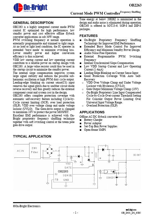
GENERAL DESCRIPTIONOB2263 is a highly integrated current mode PWM control IC optimized for high performance, low standby power and cost effective offline flybackconverter applications in sub 30W range.PWM switching frequency at normal operation is externally programmable and trimmed to tight range. At no load or light load condition, the IC operates in extended ‘burst mode’ to minimize switching loss. Lower standby power and higher conversion efficiency is thus achieved. VDD low startup current and low operating current contribute to a reliable power on startup design with OB2263. A large value resistor could thus be used in the startup circuit to minimize the standby power. The internal slope compensation improves system large signal stability and reduces the possible sub-harmonic oscillation at high PWM duty cycle output. Leading-edge blanking on current sense(CS) input removes the signal glitch due to snubber circuit diode reverse recovery and thus greatly reduces the external component count and system cost in the design. OB2263 offers complete protection coverage with automatic self-recovery feature including Cycle-by-Cycle current limiting (OCP), over load protection (OLP), VDD over voltage clamp and under voltage lockout (UVLO). The Gate-drive output is clamped to maximum 18V to protect the power MOSFET. Excellent EMI performance is achieved with On-Bright proprietary frequency shuffling technique together with soft switching control at the totem pole gate drive output. Tone energy at below 20KHZ is minimized in the design and audio noise is eliminated during operation. OB2263 is offered in SOT23-6, SOP-8 and DIP-8 packages.FEATURES ■ On-Bright Proprietary Frequency Shuffling Technology for Improved EMI Performance.■ Extended Burst Mode Control For Improved Efficiency and Minimum Standby Power Design ■ Audio Noise Free Operation ■ External Programmable PWM Switching Frequency■ Internal Synchronized Slope Compensation■ Low VDD Startup Current and Low Operating Current (1.4mA)■ Leading Edge Blanking on Current Sense Input ■ Good Protection Coverage With Auto Self-Recovery oVDD Over Voltage Clamp and Under Voltage Lockout with Hysteresis (UVLO) o Gate Output Maximum Voltage Clamp (18V) o On-Bright Proprietary Line Input Compensated Cycle-by-Cycle Over-current Threshold Setting For Constant Output Power Limiting OverUniversal Input Voltage Range. o Overload Protection (OLP) APPLICATIONS Offline AC/DC flyback converter for■ Battery Charger ■ Power Adaptor ■ Set-Top Box Power Supplies■ Open-frame SMPSTYPICAL APPLICATIONGENERAL INFORMATIONPin ConfigurationThe OB2263 is offered in SOT23-6, DIP8 and SOP8 packages, shown as below.Ordering Information Part Number DescriptionOB2263MP SOT23-6, Pb-free OB2263AP DIP8, Pb-free OB2263CP SOP8, Pb-freePackage Dissipation RatingPackageR θJA (°C/W)DIP8 90 SOP8 150SOT23-6200Absolute Maximum RatingsParameter Value VDD DC Supply Voltage30 V VDD Zener Clamp VoltageNoteVDD_Clamp+0.1VVDD DC Clamp Current 10 mA V FB Input Voltage -0.3 to 7V V SENSE Input Voltage to Sense Pin-0.3 to 7V V RI Input Voltage to RI Pin -0.3 to 7V Min/Max Operating Junction Temperature T J -20 to 150 o C Min/Max Storage Temperature T stg-55 to 160 o C Note: VDD_Clamp has a nominal value of 34V.Stresses beyond those listed under “absolute maximum ratings” may cause permanent damage to the device. These are stress ratings only, functional operation of the device at these or any other conditions beyond those indicated under “recommended operating conditions” is not implied. Exposure to absolute maximum-rated conditions for extended periods may affect device reliability.Marking InformationTERMINAL ASSIGNMENTSPin Name I/O DescriptionGND PGroundFB I Feedback input pin. The PWM duty cycle is determined by voltage level into this pin and SENSE pin input.RI I Internal Oscillator frequency setting pin. A resistor connected between RI and GND sets the PWM frequency.SENSE I Current sense input pin. Connected to MOSFET current sensing resistor node.VDD P Chip DC power supply pin.GATE O Totem-pole gate drive output for the power MOSFET.RECOMMENDED OPERATING CONDITIONSymbol Parameter MinMaxUnitVDD VDD Supply Voltage 10 to 30 VRI RI Resistor Value 100 KohmT A Operating Ambient Temperature -20 to 85 o CBLOCK DIAGRAMELECTRICAL CHARACTERISTICS(T A = 25O C if not otherwise noted)Symbol Parameter Test Conditions Min Typ Max Unit Supply Voltage (VDD) I_VDD_Startup VDD Start up Current VDD =12.5V, RI=100K Measure Leakage currentinto VDD3 20 uAI_VDD_Ops Operation Current VDD =16V,RI=100Kohm, V FB =3V1.4 mA UVLO(ON) VDD Under Voltage Lockout Enter7.8 8.8 9.8 VUVLO(OFF) VDD Under Voltage Lockout Exit (Recovery)13 14 15 VVDD_Clamp VDD Zener Clamp VoltageI VDD = 5 mA 34 VFeedback Input Section(FB Pin)A VCS PWM Input Gain ΔV FB /ΔV cs2.0 V/V V FB_Open V FB Open Loop Voltage4.8 VI FB _Short FB pin short circuit current Short FB pin to GND and measure current1.2 mAV TH _0D Zero Duty Cycle FB Threshold Voltage VDD = 16V, RI=100Kohm0.75 VV TH _PL Power Limiting FB Threshold Voltage3.7 VT D _PL Power limiting Debounce Time35 mSecZ FB _IN Input Impedance 6 Kohm DC_MAX Maximum Duty Cycle VDD=18V, RI=100Kohm, FB=3V,CS=075 %Current Sense Input(Sense Pin) T_blanking Leading edge blanking timeRI = 100 Kohm 300 nsZ SENSE _IN Input Impedance 40 Kohm T D _OC Over Current Detection andControl DelayVDD = 16V, CS>V TH _OC, FB=3.3V 75 nSecV TH _OC Over CurrentThreshold Voltage at zero Duty CycleFB=3.3V, RI=100 Kohm 0.70 0.75 0.80 V Oscillator F OSC Normal Oscillation FrequencyRI = 100 Kohm 60 65 70 KHZ∆f_TempFrequency Temperature Stability VDD = 16V, RI=100Kohm, T A -20oCto 100 o C5 % ∆f_VDDFrequency Voltage Stability VDD = 12-25V, RI=100Kohm5 % RI_range Operating RI Range 50 100 150 Kohm V_RI_open RI open load voltage 2 VF osc_BM Burst Mode BaseFrequency VDD = 16V, RI =100Kohm22 KHZGate Drive OutputVOL Output Low Level VDD = 16V, Io = -20 mA0.8 V VOH Output High Level VDD = 16V, Io = 20 mA 10 VV_Clamp OutputClampVoltage Level 18VT_r Output Rising Time VDD = 16V, CL = 1nf 220 nSec T_f Output Falling Time VDD = 16V, CL = 1nf 70 nSec Frequency Shuffling∆f_OSC FrequencyModulation range/Base frequencyRI=100K -33%f_shuffling Shuffling Frequency RI=100K 64 HZUVLO(ON) vs Temp8.08.28.48.68.89.0-20104070100130Temp(C)U V L O (O N ) (V )OPERATION DESCRIPTIONThe OB2263 is a highly integrated PWM controller IC optimized for offline flyback converter applications in sub 30W power range. The extended burst mode control greatly reduces the standby power consumption and helps the design easily meet the international power conservation requirements.•Startup Current and Start up Control Startup current of OB2263 is designed to be very low so that VDD could be charged up above UVLO threshold level and device starts up quickly. A large value startup resistor can therefore be used to minimize the power loss yet provides reliable startup in application. For AC/DC adaptor with universal input range design, a 2 MΩ, 1/8 W startup resistor could be used together with a VDD capacitor to provide a fast startup and low power dissipation solution.•Operating CurrentThe Operating current of OB2263 is low at 1.4mA. Good efficiency is achieved with OB2263 low operating current together with extended burst mode control features.•Frequency shuffling for EMI improvement The frequency Shuffling/jittering (switching frequency modulation) is implemented in OB2263. The oscillation frequency is modulated with a random source so that the tone energy is spread out. The spread spectrum minimizes the conduction band EMI and therefore reduces system design challenge.•Extended Burst Mode OperationAt zero load or light load condition, majority of the power dissipation in a switching mode power supply is from switching loss on the MOSFET transistor, the core loss of the transformer and the loss on the snubber circuit. The magnitude of power loss is in proportion to the number of switching events within a fixed period of time. Reducing switching events leads to the reduction on the power loss and thus conserves the energy.OB2263 self adjusts the switching mode according to the loading condition. At from no load to light/medium load condition, the FB input drops below burst mode threshold level. Device enters Burst Mode control. The Gate drive output switches only when VDD voltage drops below a preset level and FB input is active to output an on state. Otherwise the gate drive remains at off state to minimize the switching loss and reduces the standby power consumption to the greatest extend. The frequency control also eliminates the audio noise at any loading conditions.•Oscillator OperationA resistor connected between RI and GND sets the constant current source to charge/discharge the internal cap and thus the PWM oscillator frequency is determined. The relationship between RI and switching frequency follows the below equation within the specified RI in Kohm range at nominal loading operational condition.)()(6500KhzKohmRIFOSC=•Current Sensing and Leading Edge Blanking Cycle-by-Cycle current limiting is offered in OB2263 current mode PWM control. The switch current is detected by a sense resistor into the sense pin. An internal leading edge blanking circuit chops off the sense voltage spike at initial MOSFET on state due to Snubber diode reverse recovery so that the external RC filtering on sense input is no longer required. The current limit comparator is disabled and thus cannot turn off the external MOSFET during the blanking period. PWM duty cycle is determined by the current sense input voltage and the FB input voltage.•Internal Synchronized Slope Compensation Built-in slope compensation circuit adds voltage ramp onto the current sense input voltage for PWM generation. This greatly improves the close loop stability at CCM and prevents the sub-harmonic oscillation and thus reduces the output ripple voltage.•Gate DriveOB2263 Gate is connected to an external MOSFET gate for power switch control. Too weak the gate drive strength results in higher conduction and switch loss of MOSFET while too strong gate drive output compromises the EMI.A good tradeoff is achieved through the built-in totem pole gate design with right output strength and dead time control. The low idle loss and good EMI system design is easier to achieve with this dedicated control scheme. An internal 18V clamp is added for MOSFET gate protection at higher than expected VDD input.Current Mode PWM Controllerm kw k c om• Protection ControlsGood power supply system reliability is achieved with its rich protection features including Cycle-by-Cycle current limiting (OCP), Over Load Protection (OLP) and over voltage clamp, Under Voltage Lockout on VDD (UVLO).With On-Bright Proprietary technology, the OCP threshold tracks PWM Duty cycles and is line voltage compensated to achieve constant output power limit over the universal input voltage range with recommended reference design.At overload condition when FB input voltage exceeds power limit threshold value for more than TD_PL, control circuit reacts to shut down the output power MOSFET. Device restarts when VDD voltage drops below UVLO limit.VDD is supplied by transformer auxiliary winding output. It is clamped when VDD is higher than threshold value. The power MOSFET is shut down when VDD drops below UVLO limit and device enters power on start-up sequence thereafter.PACKAGE MECHANICAL DATASOT23-68-Pin Plastic DIP8-Pin Plastic SOPIMPORTANT NOTICERIGHT TO MAKE CHANGESOn-Bright Electronics Corp. reserves the right to make corrections, modifications, enhancements, improvements and other changes to its products and services at any time and to discontinue any product or service without notice. Customers should obtain the latest relevant information before placing orders and should verify that such information is current and complete.WARRANTY INFORMATIONOn-Bright Electronics Corp. warrants performance of its hardware products to the specifications applicable at the time of sale in accordance with its standard warranty. Testing and other quality control techniques are used to the extent it deems necessary to support this warranty. Except where mandated by government requirements, testing of all parameters of each product is not necessarily performed.On-Bright Electronics Corp. assumes no liability for application assistance or customer product design. Customers are responsible for their products and applications using On-Bright’s components, data sheet and application notes. To minimize the risks associated with customer products and applications, customers should provide adequate design and operating safeguards.LIFE SUPPORTOn-Bright Electronics Corp.’s products are not designed to be used as components in devices intended to support or sustain human life. On-bright Electronics Corp. will not be held liable for any damages or claims resulting from the use of its products in medical applications.MILITARYOn-Bright Electronics Corp.’s products are not designed for use in military applications. On-Bright Electronics Corp. will not be held liable for any damages or claims resulting from the use of its products in military applications.。
电压基准ISL60002中文资料
精密1.25V 和2.50V 低电压F G A T M 基准概述ISL60002 FGA TM 电压基准是高精度的模拟电压基准,它采用intersil 专有的浮动栅技术,可以在较低的电源电压(2.7V 到5.5V )下工作,并且工作电流极低,仅仅400nA 。
其它的特点还包括保证绝对的初始精度低至±1.0mV ,20ppm/℃的温度系数和10ppm/Hrs 000,1的长期的稳定性。
ISL60002系列的初始精度和热稳定性能,以及低电源电压和400nA 功率消耗,使它成为高分辨率,低功率数据转换系统的理想伙伴。
订购信息特点参考电压……………………………………………… 1.25V ,和2.50V绝对初始精度选项………………………………………… ±1.0mV ,±2.5mV ,和±5.0mV电源电压范围………………………………………… 2.7V 到5.5V超低电源电流…………………………………………… 400nA低20ppm/℃的温度系数10ppm/Hrs 000,1的长期的稳定性7mA 源电流和反向电流ESD 保护 ………………………………………… 5kV(人体模型)标准的8 Ld SOIC 和3 Ld SOT23封装温度范围 …………………………………………… -40℃到+85℃应用高分辨率A/D 和D/A 转换器数字仪表条形码扫描器移动通信PDA 和笔记本电池管理系统医疗系统 管脚引出线图典 型应用图引脚描述极限参数储存温度范围………………………………………………… -65℃到+125℃对GND的最大V IN……………………………………………… -0.5V至+6.5V对GND的最大V OUT(*)ISL60002,V OUT=1.25V………………………………………… -0.5V至+2.25VISL60002,V OUT=2.50V………………………………………… -0.5V至+3.50VDNC脚的电压…………………………………………………禁用引线温度,低温焊接(*) (225)(*)注:最大持续时间=10s推荐的工作条件温度范围(工业)………………………………………………………… -40℃到85℃ESD参数人体测试……………………………………………………………………5kV电气指标:ISL60002,V OUT=5V工作条件:V IN=3.0V,I OUT=0mA,C OUT=0.001μF,T A=-40到+85℃,除非另有说明。
G697L263T中文资料
6 5 4.63 4.38 4 3.30 3.08 2.93 2.63 231 219 200 165 154 146 131 70 3.3 2.3 2.2 5 1.5
V
mV
ppm/°C V
mA MΩ
Ver: 1.1 Jul 26, 2002
TEL: 886-3-5788833
Applications
Computers Controllers Intelligent Instruments Critical µP and µC Power Monitoring Portable / Battery-Powered Equipment Automotive
元器件交易网
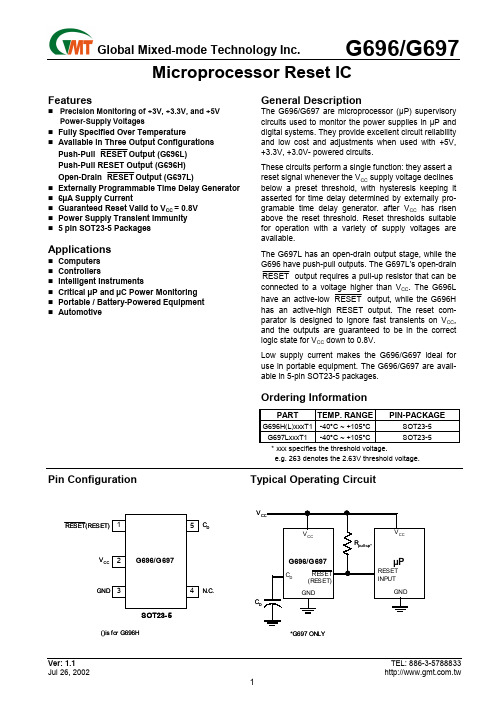
Global Mixed-mode Technology Inc.
G696/G697
Microprocessor Reset IC
Features
Precision Monitoring of +3V, +3.3V, and +5V
General Description
4 SOT23-5
N.C.
()is for G696H
*G697 ONLY
Ver: 1.1 Jul 26, 2002
TEL: 886-3-5788833
1
元器件交易网
Global Mixed-mode Technology Inc.
Power-Supply Voltages
Fully Specified Over Temperature Available in Three Output Configurations Push-Pull RESET Output (G696L) Push-Pull RESET Output (G696H) Open-Drain RESET Output (G697L) Externally Programmable Time Delay Generator 6µA Supply Current Guaranteed Reset Valid to VCC = 0.8V Power Supply Transient Immunity 5 pin SOT23-5 Packages
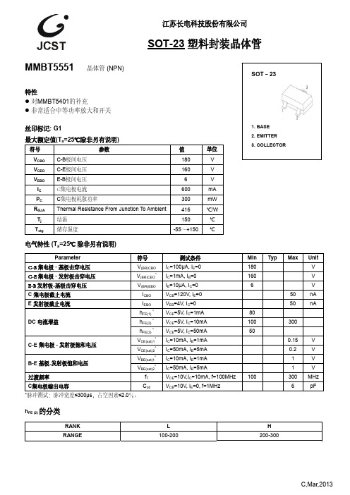
MMBT5551 G1中文数据手册
过渡频率
fT
VCE=10V,IC=10mA, f=100MHz
C集电极输出电容
Cob
VCB=10V, IE=0, f=1MHz
*脉冲测试:脉冲宽度≤300μs,占空因素≤2.0%。
1. BASE 2. EMITTER 3. COLLECTOR
Min Typ Max Unit
180
V
160
V
6
V
50
nA
hFE(2) *
VCE=5= V, IC 10mA
hFE(3) *= VCE=5V, IC 50mA
VCE(sat)1* = IC=10mA, IB 1mA
VCE(sat)2* = IC=50mA, IB 5mA
VBE(sat)1* = IC=10mA, IB 1mA
VBE(sat)2* = IC=50mA, IB 5mA
50
nA
80
100
300
50
0.15
V
0.2
V
1
V
1
V
100
300 MHz
6
pF
hFE (2) 的分类
RANK RANGE
L 100-200
H 200-300
C,Mar,2013
典型特性
集电极电流 IC (mA)
Static Characteristic
18
90uA
COMMON
EMITTER
15
80uA
——
200
IC
COMMON EMITTER
100 VCE=5V
Ta=100℃
Ta=25℃
10
100 200
集电极电流 IC (mA)
SCI 高性能 NPN 双极性晶体管 2N4921G、2N4922G、2N4923G 数据手册说明书

2N4921G, 2N4922G,2N4923GMedium-Power PlasticNPN Silicon TransistorsThese high−performance plastic devices are designed for driver circuits, switching, and amplifier applications.Features•Low Saturation V oltage•Excellent Power Dissipation•Excellent Safe Operating Area•Complement to PNP 2N4920G•These Devices are Pb−Free and are RoHS Compliant** MAXIMUM RATINGSRating Symbol Value UnitCollector−Emitter Voltage 2N4921G2N4922G2N4923G V CEO406080VdcCollector−Emitter Voltage 2N4921G2N4922G2N4923G V CB406080VdcEmitter Base Voltage V EB 5.0VdcCollector Current − Continuous (Note 1)I C 1.0Adc Collector Current − Peak (Note 1)I CM 3.0Adc Base Current − Continuous I B 1.0AdcTotal Power Dissipation @ T C = 25_C Derate above 25_C PD300.24WmW/_COperating and Storage JunctionTemperature RangeT J, T stg–65 to +150_CStresses exceeding those listed in the Maximum Ratings table may damage the device. If any of these limits are exceeded, device functionality should not be assumed, damage may occur and reliability may be affected.1.The 1.0 A maximum I Cvalue is based upon JEDEC current gain requirements.The 3.0 A maximum value is based upon actual current handling capability of the device (see Figures 5 and 6).THERMAL CHARACTERISTICS (Note 2)Characteristic Symbol Max Unit Thermal Resistance, Junction−to−Case R q JC 4.16_C/W 2.Recommend use of thermal compound for lowest thermal resistance.*Indicates JEDEC Registered Data.*For additional information on our Pb−Free strategy and soldering details, please download the ON Semiconductor Soldering and Mounting Techniques Reference Manual, SOLDERRM/D.1.0 AMPEREGENERAL PURPOSEPOWER TRANSISTORS40−80 VOLTS, 30 WATTSMARKING DIAGRAMY=YearWW=Work Week2N492x=Device Codex = 1, 2, or 3G=Pb−Free PackageDevice Package Shipping ORDERING INFORMATION2N4921G TO−225(Pb−Free)500 Units / Box2N4922G TO−225(Pb−Free)500 Units / Box2N4923G TO−225(Pb−Free)500 Units / Box3EMITTERCOLLECTORTO−225CASE 77−09STYLE 13YWW2N492xGELECTRICAL CHARACTERISTICS (T C= 25_C unless otherwise noted)Characteristic Symbol Min Max Unit OFF CHARACTERISTICSCollector−Emitter Sustaining Voltage (Note 3) (I C = 0.1 Adc, I B = 0)2N4921G2N4922G2N4923G V CEO(sus)406080−−−VdcCollector Cutoff Current (V CE = 20 Vdc, I B = 0)2N4921G(V CE = 30 Vdc, I B = 0)2N4922G(V CE = 40 Vdc, I B = 0)2N4923G I CEO−−−0.50.50.5mAdcCollector Cutoff Current(V CE = Rated V CEO, V EB(off) = 1.5 Vdc)(V CE = Rated V CEO, V EB(off) = 1.5 Vdc, T C = 125_C I CEX−−0.10.5mAdcCollector Cutoff Current (V CB = Rated V CB, I E = 0)I CBO−0.1mAdcEmitter Cutoff Current (V EB = 5.0 Vdc, I C = 0)I EBO− 1.0mAdcON CHARACTERISTICSDC Current Gain (Note 3)(I C = 50 mAdc, V CE = 1.0 Vdc) (I C = 500 mAdc, V CE = 1.0 Vdc) (I C = 1.0 Adc, V CE = 1.0 Vdc)h FE403010−150−−Collector−Emitter Saturation Voltage (Note 3) (I C = 1.0 Adc, I B = 0.1 Adc)V CE(sat)−0.6VdcBase−Emitter Saturation Voltage (Note 3) (I C = 1.0 Adc, I B = 0.1 Adc)V BE(sat)− 1.3VdcBase−Emitter On Voltage (Note 3) (I C = 1.0 Adc, V CE = 1.0 Vdc)V BE(on)− 1.3VdcSMALL−SIGNAL CHARACTERISTICSCurrent−Gain − Bandwidth Product(I C = 250 mAdc, V CE = 10 Vdc, f = 1.0 MHz)f T3.0−MHzOutput Capacitance(V CB = 10 Vdc, I E = 0, f = 100 kHz)C ob−100pFSmall−Signal Current Gain(I C = 250 mAdc, V CE = 10 Vdc, f = 1.0 kHz)h fe25−−Product parametric performance is indicated in the Electrical Characteristics for the listed test conditions, unless otherwise noted. Product performance may not be indicated by the Electrical Characteristics if operated under different conditions.3.Pulse Test: PW ≈ 300 m s, Duty Cycle ≈ 2.0%.40302010255075100125150Figure 1. Power DeratingT C , CASE TEMPERATURE (°C)P D , P O W E R D I S S I P A T I O N (W A T T S )Safe Area Curves are indicated by Figure 5. All limits are applicable and must be observed.Figure 2. Switching Time Equivalent Circuit5.0Figure 3. Turn −On TimeI C , COLLECTOR CURRENT (mA)t , T I M E ( s )μ 2.01.00.70.50.30.20.10.052.0%0.073.0V BE(off)V in V TURN-OFF PULSEobtain desired current levelsFigure 4. Thermal Responset, TIME (ms)1.00.010.70.50.30.20.10.070.050.030.02r (t ), T R A N S I E N T T H E R M A LR E S I S T A N C E (N O R M A L I Z E D )10Figure 5. Active −Region Safe Operating AreaV CE , COLLECTOR-EMITTER VOLTAGE (VOLTS)5.02.01.00.50.10.2I C , C O L L E C T O R C U R R E N T (A M P )7.03.00.70.3There are two limitations on the power handling ability of a transistor: average junction temperature and second breakdown. Safe operating area curves indicate I C − V CE operation i.e., the transistor must not be subjected to greater dissipation than the curves indicate.The data of Figure 5 is based on T J(pk) = 150_C; T C is variable depending on conditions. Second breakdown pulse limits are valid for duty cycles to 10% provided T J(pk) ≤ 150_C. At high case temperatures, thermal limitations will reduce the power that can be handled to values less than the limitations imposed by second breakdown.t μs , S T O R A G E T I M E ( s )′5.0Figure6. Storage Time I C , COLLECTOR CURRENT (mA)2.01.00.50.30.20.10.050.073.00.75.0Figure 7. Fall TimeI C , COLLECTOR CURRENT (mA)2.01.00.50.30.20.10.050.073.00.7t μf , F A L L T I M E ( s )V C E , C O L L E C T O R -E M I T T E R V O L T A G E (V O L T S )R B E , E X T E R N A L B A S E -E M I T T E R R E S I S T A N C E (O H M S )1000Figure 8. Current GainI C , COLLECTOR CURRENT (mA)1050020010070Figure 9. Collector Saturation Region1.0I B , BASE CURRENT (mA)0.80.60.40.2700300h F E , D C C U R R E N T G A I N503020108Figure 10. Effects of Base −Emitter Resistance T J , JUNCTION TEMPERATURE (°C)1071051041031061.5I C , COLLECTOR CURRENT (mA)1.20.90.60.3V O L T A G E (V O L T S )Figure 11. “On” Voltage104Figure 12. Collector Cut −Off Region V BE , BASE-EMITTER VOLTAGE (VOLTS)10310210-1, C O L L E C T O R C U R R E N T ( A )μI C + 2.5Figure 13. Temperature CoefficientsI C , COLLECTOR CURRENT (mA)T E M P E R A T U R E C O E F F I C I E N T S (m V /C )°+ 2.0+ 1.5+ 0.50- 0.5- 1.0- 1.5- 2.0- 2.5+ 1.010110010- 2TO −225CASE 77−09ISSUE ADDATE 25 MAR 2015STYLE 1:PIN 1.EMITTER 2., 4.COLLECTOR 3.BASE STYLE 6:PIN 1.CATHODE 2., 4.GATE 3.ANODESTYLE 2:PIN 1.CATHODE 2., 4.ANODE 3.GATE STYLE 3:PIN 1.BASE2., 4.COLLECTOR3.EMITTER STYLE 4:PIN 1.ANODE 12., 4.ANODE 23.GATE STYLE 5:PIN 1.MT 12., 4.MT 23.GATE STYLE 7:PIN 1.MT 12., 4.GATE 3.MT 2STYLE 8:PIN 1.SOURCE 2., 4.GATE 3.DRAINSTYLE 9:PIN 1.GATE 2., 4.DRAIN 3.SOURCESTYLE 10:PIN 1.SOURCE 2., 4.DRAIN 3.GATEYWW XXXXXXXGY = Year WW = Work Week XXXXX = Device Code G = Pb −Free Package*This information is generic. Please refer to device data sheet for actual part marking.Pb −Free indicator, “G” or microdot “ G ”,may or may not be present.GENERICMARKING DIAGRAM*SCALE 1:1DIM MIN MAX MILLIMETERS D 10.6011.10E 7.407.80A 2.40 3.00b 0.600.90P 2.90 3.30L1 1.27 2.54c 0.390.63L 14.5016.63b20.510.88Q3.804.20A1 1.00 1.50e 2.04 2.54NOTES:1.DIMENSIONING AND TOLERANCING PER ASME Y14.5M, 1994.2.CONTROLLING DIMENSION: MILLIMETERS.3.NUMBER AND SHAPE OF LUGS OPTIONAL.FRONT VIEWBACK VIEWFRONT VIEWSIDE VIEW31MECHANICAL CASE OUTLINEPACKAGE DIMENSIONSON Semiconductor and are trademarks of Semiconductor Components Industries, LLC dba ON Semiconductor or its subsidiaries in the United States and/or other countries.ON Semiconductor reserves the right to make changes without further notice to any products herein. ON Semiconductor makes no warranty, representation or guarantee regarding the suitability of its products for any particular purpose, nor does ON Semiconductor assume any liability arising out of the application or use of any product or circuit, and specifically disclaims any and all liability, including without limitation special, consequential or incidental damages. ON Semiconductor does not convey any license under its patent rights nor theON Semiconductor and are trademarks of Semiconductor Components Industries, LLC dba ON Semiconductor or its subsidiaries in the United States and/or other countries.ON Semiconductor owns the rights to a number of patents, trademarks, copyrights, trade secrets, and other intellectual property. A listing of ON Semiconductor’s product/patent coverage may be accessed at ON Semiconductor makes no warranty, representation or guarantee regarding the suitability of its products for any particular purpose, nor does ON Semiconductor assume any liability arising out of the application or use of any product or circuit, and specifically disclaims any and all liability, including without limitation special, consequential or incidental damages.PUBLICATION ORDERING INFORMATIONTECHNICAL SUPPORTNorth American Technical Support:Voice Mail: 1 800−282−9855 Toll Free USA/Canada Phone: 011 421 33 790 2910LITERATURE FULFILLMENT :Email Requests to:*******************ON Semiconductor Website: Europe, Middle East and Africa Technical Support:Phone: 00421 33 790 2910For additional information, please contact your local Sales Representative。
ST GM5621, GM5626, GM2621 数据手册

Data BriefFor further information contact your local STMicroelectronics sales office.October 2008 Rev 11/8GM5621, GM5626, GM2621Dual input LCD controller for entry level applicationsFeatures■Zoom (from VGA) and shrink (from UXGA) scaling■Triple-channel (8-bit) ADC and PLL ■Ultra-Reliable DVI® receiver (165 MHz)—DVI 1.0-compliant■Dual channel RSDS transmitter and TCON (GM5626 only)■Dual channel LVDS transmitter■Intel x86 compatible microcontroller with external SPI ROM interface■Versatile OSD engine meets PC OEM specs ■All system clocks synthesized from a single external crystal■Digital color controls and sRGB compliant■10-bit panel gamma correction and high quality dithering for 8-bit and 6-bit panel interface ■DDC controller for host interface purposes ■Low bandwidth ADC for keypad interface and cable detection■Two Pulse Width Modulation (PWM) signals for backlight and volume control■Internal test pattern generator for factory test purposes■Energy Spectrum Management® (ESM®)■Instant Auto™ Image AdjustmentApplication■Mainstream analog and dual-input XGA/SXGA/WXGA LCD monitorsDescription GM5621, GM5626, GM2621 1 DescriptionGenesis GM5621 and GM5626 are all-in-one dual input LCD monitor controllers supportingresolutions up to SXGA/WXGA, available in a very low pin count package. GM5621/5626leverage Genesis patented advanced image-processing technology, as well as a provenintegrated ADC/PLL and an Ultra-Reliable DVI compliant digital receiver to deliver a high-quality solution for mainstream analog and dual input monitors. GM5621/5626 offer newInstant Auto technology, which provides fast and accurate image alignment for both staticand moving images of the analog input signal. GM5621 includes an on-chip, industrystandard, dual channel LVDS transmitter and a TCON, and GM5626 includes a dualchannel RSDS transmitter for direct interfacing of commercially available LVDS/RSDS LCDpanel modules.In addition, GM5621/5626 include an integrated x86 OCM with SPI compatible interface, amulticolor proportional font OSD engine, a programmable coefficient scaling engine, dualchannel Schmitt and Reset circuitry. Along with high quality and reliability, GM5621/5626also provide a very low cost system design by reducing the number of components and thereduction in the board size.GM2621 is a pin-compatible analog derivative product with integrated ADC/PLL, but no DVIreceiver.2/8GM5621, GM5626, GM2621Description3/8Feature attributes GM5621, GM5626, GM26214/82 Feature attributes●Analog RGB input –Supports up to SXGA/WXGA 75 Hz/UXGA 60 Hz –Composite-sync and Sync-on-Green (SOG) support –Input format detection and auto-alignment –Phase clock and image positioning●Instant Auto image adjustment –Faster and more accurate than current conventional methods –Auto-adjusts full width and partial width images–Auto-adjusts DOS screens and moving images, such as screen savers and motionpictures●Ultra-reliable DVI input (GM5621/5626)–Operating speed 165 MHz (up to UXGA 60 Hz)–Direct connect to all DVI-compliant digital transmitters –High-bandwidth Digital Content Protection (HDCP)●Intelligent Image Processing™–Programmable coefficients for user sharpness control–Real Recovery™ function provides full color recovery image for refresh rates higher than those supported by the LCD panel●On-chip microcontroller –High-performance x86 MCU with on-chip RAM and ROM –Unified memory architecture simplifies chip programming –Five general-purpose outputs (GPO) –UART link for ISP and factory setting purpose –Two DDC2Bi with DMA buffer to internal RAM–Slow clock mode for 50mW sleep mode power consumption –JTAG support for firmware debugging●On-chip OSD controller –On-chip RAM for high-quality programmable menus –1, 2, and 4-bit per pixel character cells –Horizontal and vertical stretch of OSD menus –Blinking, transparency and blending–Supports two independent OSD menu rectangles –Proportional fonts●LVDS transmitters –Double pixel up to SXGA/WXGA 75 Hz output –Support for 8/6-bit panels (with high-quality dithering)–Pin swap, odd or even swap and red or blue group swap of RGB outputs for flexibility in board layout –Programmable signal amplitudeGM5621, GM5626, GM2621Feature attributes●RSDS transmitters and TCON (GM5626)–Dual channel 6-bit RSDS compliant serial interface with direct connect to RSDS compliant column drivers–Support for type 1, type 2, and type 3 bus configuration–Pin swap, odd or even swap and red or blue group swap of RGB outputs forflexibility in board layout–Low EMI and power save feature include frame, line and in-line inversion andblanking●Highly integrated system-on-a-chip–50mW power saving mode–5-volt tolerant inputs–Two layer PCB support–On-chip reset circuit to eliminate external reset IC–Integrated Schmitt trigger for HSYNC and VSYNC–General purpose low bandwidth ADC5/8Ordering information GM5621, GM5626, GM26216/83 Ordering informationIn order to meet environmental requirements, ST offers these devices in ECOPACK®packages. These packages have a lead-free second level interconnect. The category of second level interconnect is marked on the package and on the inner box label, in compliance with JEDEC Standard JESD97. The maximum ratings related to soldering conditions are also marked on the inner box label. ECOPACK is an ST trademark. ECOPACK specifications are available at .Table 1.Order codesPart numberDescriptionGM2621-LF-AA 128-pin PQFP GM2621-LF-BC 128-pin PQFP GM2621-LF-CD 128-pin PQFP GM5621-LF-AA 128-pin PQFP GM5621-LF-CD 128-pin PQFP GM5626-LF-AA 128-pin PQFP GM5626H-LF-AA128-pin PQFPGM5621, GM5626, GM2621Revision history7/84 Revision historyTable 2.Document revision historyDate RevisionChanges09-Oct-20081Initial release.GM5621, GM5626, GM26218/8Please Read Carefully:Information in this document is provided solely in connection with ST products. STMicroelectronics NV and its subsidiaries (“ST”) reserve the right to make changes, corrections, modifications or improvements, to this document, and the products and services described herein at any time, without notice.All ST products are sold pursuant to ST’s terms and conditions of sale.Purchasers are solely responsible for the choice, selection and use of the ST products and services described herein, and ST assumes no liability whatsoever relating to the choice, selection or use of the ST products and services described herein.No license, express or implied, by estoppel or otherwise, to any intellectual property rights is granted under this document. If any part of this document refers to any third party products or services it shall not be deemed a license grant by ST for the use of such third party products or services, or any intellectual property contained therein or considered as a warranty covering the use in any manner whatsoever of such third party products or services or any intellectual property contained therein.UNLESS OTHERWISE SET FORTH IN ST’S TERMS AND CONDITIONS OF SALE ST DISCLAIMS ANY EXP RESS OR IMP LIED WARRANTY WITH RESP ECT TO THE USE AND/OR SALE OF ST P RODUCTS INCLUDING WITHOUT LIMITATION IMP LIED WARRANTIES OF MERCHANTABILITY, FITNESS FOR A PARTICULAR PURPOSE (AND THEIR EQUIVALENTS UNDER THE LAWS OF ANY JURISDICTION), OR INFRINGEMENT OF ANY PATENT, COPYRIGHT OR OTHER INTELLECTUAL PROPERTY RIGHT. UNLESS EXP RESSLY AP P ROVED IN WRITING BY AN AUTHORIZED ST REP RESENTATIVE, ST P RODUCTS ARE NOT RECOMMENDED, AUTHORIZED OR WARRANTED FOR USE IN MILITARY, AIR CRAFT, SPACE, LIFE SAVING, OR LIFE SUSTAINING APPLICATIONS, NOR IN PRODUCTS OR SYSTEMS WHERE FAILURE OR MALFUNCTION MAY RESULT IN PERSONAL INJURY, DEATH, OR SEVERE PROPERTY OR ENVIRONMENTAL DAMAGE. ST PRODUCTS WHICH ARE NOT SPECIFIED AS "AUTOMOTIVE GRADE" MAY ONLY BE USED IN AUTOMOTIVE APPLICATIONS AT USER’S OWN RISK.Resale of ST products with provisions different from the statements and/or technical features set forth in this document shall immediately void any warranty granted by ST for the ST product or service described herein and shall not create or extend in any manner whatsoever, any liability of ST.ST and the ST logo are trademarks or registered trademarks of ST in various countries.Information in this document supersedes and replaces all information previously supplied.The ST logo is a registered trademark of STMicroelectronics. All other names are the property of their respective owners.© 2008 STMicroelectronics - All rights reservedSTMicroelectronics group of companiesAustralia - Belgium - Brazil - Canada - China - Czech Republic - Finland - France - Germany - Hong Kong - India - Israel - Italy - Japan - Malaysia - Malta - Morocco - Singapore - Spain - Sweden - Switzerland - United Kingdom - United States of America。
2026-35-C2F,2026-23-ALF,2026-26-ALF,2026-35-ALF,2026-60-ALF,2026-15-A1LF, 规格书,Datasheet 资料
*RoHS Directive 2002/95/EC Jan 27, 2003 including Annex. Specifi cations are subject to change without notice.Customers should verify actual device performance in their specifi c applications.Test Methods per ITU-T (CCITT) K.12, IEEE C62.31, RUS PE-80, Telcordia GR 1361CharacteristicModel No.2026-072026-092026-152026-202026-232026-252026-26DC Sparkover ±20 % @ 100 V/s 75 V 90 V 150 V 200 V 230 V 250 V 260V 1Impulse Sparkover 100 V/µs 1000 V/µs 275 V 700 V275 V 600 V350 V 575 V425 V 625 V450 V 650 V475 V 700 V475 V 700 VImpulse Transverse Delay .............................................1000 V/µs .................................................................< 75 ns Insulation Resistance ...................................................100 V (50 V for Model 2026–07 & 2026-09) .............> 1010 Ω Glow Voltage ................................................................10 mA .......................................................................~ 70 V Arc Voltage ...................................................................1A .............................................................................~ 10 V Glow-Arc Transition Current ...........................................................................................................................< 0.5 A Capacitance .................................................................1 MHz .......................................................................< 2 pF DC Holdover Voltage 2 .................................................>135 V , (52 V for Model 2026-07 & 2026-09, ...........< 150 ms 80 V for Model 2026-15)Impulse Discharge Current ...........................................40000 A, 8/20 µs 3 .................................................... 1 operation minimum 20000 A, 8/20 µs ......................................................> 10 operations 5000 A, 10/350 µs ................................................... 1 operation 1000 A, 10/1000 µs .................................................> 400 operationsAlternating Discharge Current ......................................130 Arms, 11 cycles 3 ............................................... 1 operation minimum 20 Arms, 1 s .............................................................> 10 operations Operation and Storage Temperature .............................................................................................................. -40 to +90 °C Climatic Category (IEC 60068-1) .................................................................................................................... 40/ 90/ 21Optional Switch-Grade Fail-short device available.Notes:• UL recognized component, UL File E153537.• Model number marking on tube: 26-xxx V .• The rated discharge current for TRIGARD ® Gas Discharge Tubes is the total current equally divided between each line to ground. • Sparkover limits after life ±25 %, IR >108Ω (-25 %,+30 % for Model 2026-07, 2026-09 and 2026-60).• Line to Line voltage is approximately 1.8 to 2 times the stated Line to Ground breakdown voltage.• At delivery AQL 0.65 Level II, DIN ISO 28591 Tube meets BT requirement Type 14 A/1 (210-310 V).2 Network applied.3 DC Sparkover may exceed ±25 % after discharge, but will continue to protect without venting.*R o H S C O M P L I A N T V E R S I O N S A V A I L A B L ECharacteristicModel No.2026-302026-352026-402026-422026-472026-60DC Sparkover ±20 % @ 100 V/s 300 V 350 V 400 V 420 V 470 V 600 V Impulse Sparkover 100 V/µs 1000 V/µs500 V 775 V625 V 875 V675 V 925 V725 V 1000 V800 V 1100 V925 V 1250 VSpecifi cations are subject to change without notice.Customers should verify actual device performance in their specifi c applications.Product Dimensions (additional lead form confi gurations available upon request)How to Order2026 - nn - x n F LFModel Number DesignatorVoltage (Divided by 10) 07 = 75 V 30 = 300 V 09 = 90 V 35 = 350 V 15 = 150 V 40 = 400 V 20 = 200 V 42 = 420 V 23 = 230 V 47 = 470 V 25 = 250 V 60 = 600 V 26 = 260 V LeadsA = None C = 1 mmLead Shape(See Product Dimension Drawings) Fail-Short OptionBlank = Standard Product F = With Fail-Short MechanismRoHS Compliant Option Blank = S tandard ProductLF = RoHS Compliant Product2026-XX-ADIMENSIONS: MILLIMETERSUNITS WITH LEADS ARE BASED ON THE2026-XX-A1 BODY .2026-XX-A12026-XX-C22026-XX-C32026-XX-C42026-XX-C82026-XX-C1.0 mm dia. lead wireFAIL-SHORT CONFIGURATION2026-XX-C2F SHOWNREV . 04/11Specifi cations are subject to change without notice.Customers should verify actual device performance in their specifi c applications.Switch-Grade Fail-short Device Shorting Curve 2026-XX-XF10.020.030.05.0C u r r e n t (A ) (E L T G S )1.00.50.1110100ELTGS = Each Line to Ground SimultaneouslyNOTE: When using a GDT fail-short device, it is imperative that all components associated and connected to the GDT with failsafe be tested in their respective completely integrated environment (finished product) to assure desired operation.Seconds1000。
G2302中文资料
ISSUED DATE :2004/07/06 REVISED DATE :2005/03/14BG 2302N -C H A N N E L E N H A N C E M E N T M O D E P O W E R M O S F E TDescription The G2302 provide the designer with best combination of fast switching, low on-resistance and cost-effectiveness.Features*Capable of 2.5V gate drive *Small Package OutlineMillimeter Millimeter REF . Min. Max. REF . Min. Max. A 2.70 3.10 G1.90 REF . B2.40 2.80 H 1.00 1.30 C 1.40 1.60 K 0.10 0.20 D 0.35 0.50 J 0.40 - E 0 0.10 L 0.85 1.15M10 Unit V V A A A W W/ Thermal Data ParameterSymbol Ratings Unit Thermal Resistance Junction-ambient 3Max.Rthj-a90/WBV DSS 20V R DS(ON) 85m I D 3.2APb Free Plating ProductElectrical Characteristics(Tj = 25 Unless otherwise specified)ParameterSymbol Min. Typ. Max. Unit Test Conditions Drain-Source Breakdown VoltageBV DSS20 - - VV GS =0, I D =250uABreakdown Voltage Temperature CoefficientBV DSS /Tj- 0.1 - V/ Reference to 25 , I D =1mA Gate Threshold Voltage V GS(th) 0.5 - 1.2 V V DS =V GS , I D =250uA Forward Transconductance g fs - 6 - S V DS =5V, I D =3.6A Gate-Source Leakage CurrentI GSS - - 100 nA V GS = 12V Drain-Source Leakage Current(Tj=25 ) - - 1 uA V DS =20V, V GS =0 Drain-Source Leakage Current(Tj=70 )I DSS- - 10 uA V DS =20V, V GS =0 - - 85 V GS =4.5V, I D =3.6A Static Drain-Source On-Resistance 2R DS(ON) - - 115 mV GS =2.5V, I D =3.1A Total Gate Charge 2 Q g - 4.4 - Gate-Source Charge Q gs - 0.6 - Gate-Drain (“Miller”) Change Q gd - 1.9 - nCI D =3.6A V DS =10V V GS =4.5V Turn-on Delay Time 2 T d(on) - 5.2 - Rise TimeT r - 37 - Turn-off Delay Time T d(off) - 15 - Fall Time T f - 5.7 - nsV DS =10V I D =3.6A V GS =5V R G =6 R D =2.8 Input Capacitance C iss - 145 - Output CapacitanceC oss - 100 - Reverse Transfer CapacitanceC rss-50-pFV GS =0V V DS =10V f=1.0MHzSource-Drain DiodeParameterSymbol Min. Typ. Max. Unit Test Conditions Forward On Voltage 2V SD - - 1.2 V I S =1.6A, V GS =0V Continuous Source Current (Body Diode ) I S - - 1 A V D = V G =0V, V S =1.2V Pulsed Source Current (Body Diode )1I SM--10ANotes: 1. Pulse width limited by Max. junction temperature. 2. Pulse width 300us, duty cycle 2%.3. Surface mounted on 1 in 2 copper pad of FR4 board;270 /W when mounted on min. copper pad.Characteristics CurveFig 5. Forward Characteristics of Reverse Diode Fig 1. Typical Output Characteristics Fig 2. Typical Output CharacteristicsFig 3. On-Resistance v.s. Gate VoltageFig 4. Normalized On-Resistancev.s. Junction TemperatureFig 6. Gate Threshold Voltage v.s.Junction TemperatureFig 9. Maximum Safe Operating Area Fig 10. Effective Transient Thermal ImpedanceFig 7. Gate Charge Characteristics Fig 8. Typical Capacitance CharacteristicsFig 11. Switching Time WaveformFig 12. Gate Charge Waveform。
GP2S60A中文资料
NOTICEq The circuit application examples in this publication are provided to explain representative applications of SHARP devices and are not intended to guarantee any circuit design or license any intellectual property rights. SHARP takes no responsibility for any problems related to any intellectual property right of a third party resulting from the use of SHARP's devices.q Contact SHARP in order to obtain the latest device specification sheets before using any SHARP device. SHARP reserves the right to make changes in the specifications, characteristics, data, materials, structure, and other contents described herein at any time without notice in order to improve design or reliability. Manufacturing locations are also subject to change without notice.q Observe the following points when using any devices in this publication. SHARP takes no responsibility for damage caused by improper use of the devices which does not meet the conditions and absolute maximum ratings to be used specified in the relevant specification sheet nor meet the following conditions:(i)The devices in this publication are designed for use in general electronic equipment designs such as:--- Personal computers--- Office automation equipment--- Telecommunication equipment [terminal]--- Test and measurement equipment--- Industrial control--- Audio visual equipment--- Consumer electronics(ii)Measures such as fail-safe function and redundant design should be taken to ensure reliability and safety when SHARP devices are used for or in connection with equipment that requires higher reliability such as:--- Transportation control and safety equipment (i.e., aircraft, trains, automobiles, etc.)--- Traffic signals--- Gas leakage sensor breakers--- Alarm equipment--- Various safety devices, etc.(iii)SHARP devices shall not be used for or in connection with equipment that requires an extremely high level of reliability and safety such as:--- Space applications--- Telecommunication equipment [trunk lines]--- Nuclear power control equipment--- Medical and other life support equipment (e.g., scuba).q Contact a SHARP representative in advance when intending to use SHARP devices for any "specific" applications other than those recommended by SHARP or when it is unclear which category mentioned above controls the intended use.q If the SHARP devices listed in this publication fall within the scope of strategic products described in the Foreign Exchange and Foreign Trade Control Law of Japan, it is necessary to obtain approval to export such SHARP devices. q This publication is the proprietary product of SHARP and is copyrighted, with all rights reserved. Under the copyright laws, no part of this publication may be reproduced or transmitted in any form or by any means, electronic or mechanical, for any purpose, in whole or in part, without the express written permission of SHARP. Express written permission is also required before any use of this publication may be made by a third party.q Contact and consult with a SHARP representative if there are any questions about the contents of this publication.。
AP60L02P中文资料
N-CHANNEL ENHANCEMENT MODE POWER MOSFETAbsolute Maximum RatingsSymbol Units V DS V V GSV I D @T C =25℃A I D @T C =100℃A I DMA P D @T C =25℃W W/℃T STG ℃T J℃Symbol Value Unit Rthj-case Thermal Resistance Junction-case Max. 2.0℃/W Rthj-ambThermal Resistance Junction-ambientMax.62℃/WData & specifications subject to change without notice200218032Thermal DataParameterPulsed Drain Current 1180Operating Junction Temperature Range-55 to 150Linear Derating Factor 0.5Storage Temperature RangeTotal Power Dissipation 62.5-55 to 150Continuous Drain Current, V GS @ 10V 50Continuous Drain Current, V GS @ 10V 32Drain-Source Voltage 25Gate-Source VoltageAP60L02S/PParameterRating ± 20G DSTO-263(S)GDS TO-220(P)Electrical Characteristics@T j =25o C(unless otherwise specified)Symbol ParameterTest ConditionsMin.Typ.Max.Units BV DSSDrain-Source Breakdown VoltageV GS =0V, I D =250uA 25--V ΔB V DSS /ΔT jBreakdown Voltage Temperature Coefficient Reference to 25℃, I D =1mA-0.037-V/℃R DS(ON)Static Drain-Source On-Resistance V GS =10V, I D =25A --12m ΩV GS =4.5V, I D =20A --26m ΩV GS(th)Gate Threshold Voltage V DS =V GS , I D =250uA 1-3V g fs Forward TransconductanceV DS =10V, I D =25A -30-S I DSS Drain-Source Leakage Current (T j =25o C)V DS =25V, V GS =0V --1uA Drain-Source Leakage Current (T j =150o C)V DS =20V, V GS =0V --25uA I GSS Gate-Source Leakage V GS =--nA Q g Total Gate Charge 2I D =25A -21nC Q gs Gate-Source Charge V DS =20V - 2.8nC Q gd Gate-Drain ("Miller") Charge V GS =5V -16nC t d(on)Turn-on Delay Time 2V DS =15V -8-ns t r Rise TimeI D =20A-75-ns t d(off)Turn-off Delay Time R G =3.3Ω,V GS =10V -22-ns t f Fall Time R D =0.75Ω-20-ns C iss Input Capacitance V GS =0V -605-pF C oss Output CapacitanceV DS =25V -415-pF C rssReverse Transfer Capacitancef=1.0MHz-195-pFSource-Drain DiodeSymbol ParameterTest ConditionsMin.Typ.Max.Units I S Continuous Source Current ( Body Diode )V D =V G =0V , V S =1.26V --50A I SM Pulsed Source Current ( Body Diode )1--180A V SDForward On Voltage 2T j =25℃, I S =50A, V GS =0V--1.26VNotes:1.Pulse width limited by safe operating area.2.Pulse width <300us , duty cycle <2%.AP60L02S/P±100± 20VAP60L02S/PFig 1. Typical Output Characteristics Fig 2. Typical Output CharacteristicsFig 3. On-Resistance v.s. Gate VoltageFig 4. Normalized On-Resistancev.s. Junction TemperatureAP60L02S/PFig 5. Maximum Drain Current v.s. Fig 6. Typical Power DissipationCase TemperatureFig 7. Maximum Safe Operating AreaFig 8. Effective Transient Thermal ImpedanceAP60L02S/PFig 9. Gate Charge Characteristics Fig 10. Typical Capacitance CharacteristicsReverse DiodeJunction TemperatureAP60L02S/PFig 13. Switching Time Circuit Fig 14. Switching Time WaveformFig 15. Gate Charge Circuit Fig 16. Gate Charge Waveform。