Hard Switching Process Optimization for Selected Transistor Suited for High Power and High Frequ
FDN338中文资料
FDN338P Rev.D
元器件交易网
Typical Electrical Characteristics
5 -V GS , GATE-SOURCE VOLTAGE (V) 1000
0.5 0.46 -55 to 150
W
Operating and Storage Temperature Range
°C
THERMAL CHARACTERISTICS Thermal Resistance, Junction-to-Ambient Thermal Resistance, Junction-to-Case
FDN338P Rev.D
元器件交易网
Typical Electrical Characteristics
10 -I D , DRAIN-SOURCE CURRENT (A) 2
RDS(ON) , NORMALIZED
8
VGS = -4.5V -4.0 -3.5
-3.0 -2.5
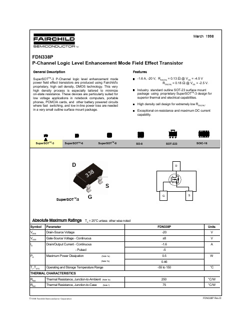
SuperSOTTM-3
SuperSOTTM-6
SuperSOTTM-8
SO-8
SOT-223
SOIC-16
D
D
8 33
S
SuperSOT -3
TM
G
G
S
Absolute Maximum Ratings
Symbol VDSS VGSS ID PD TJ,TSTG RθJA RθJC Parameter Drain-Source Voltage
元器件交易网
March 1998
FDN338P P-Channel Logic Level Enhancement Mode Field Effect Transistor
XR1002-QB资料

18.0-30.0 GHz GaAs Receiver QFN, 7x7 mmFundamental High Dynamic Range Receiver Integrated Gain Control+4.0 dBm Input Third Order Intercept (IIP3)FeaturesNovember 2006 - Rev 03-Nov-0618.0-30.0 GHz GaAs ReceiverQFN, 7x7 mmReceiver MeasurementsNovember 2006 - Rev 03-Nov-06I R (d B c )182022242628303234RF (GHz) [IF=2GHz]I I P 3 (d B m )182022242628303234RF (GHz) [IF=2GHz]G a i n (d B )18.0-30.0 GHz GaAs ReceiverQFN, 7x7 mmReceiver Measurements (cont.)November 2006 - Rev 03-Nov-06XR1002-QB, USB Noise Figure (dB) Over TemperatureN F (d B )18.0-30.0 GHz GaAs ReceiverQFN, 7x7 mmPhysical DimensionsPin Designations(Note: Engineering designator is 30KRP_03A)Pin NumberPin Name Pin Function Nominal Value Unit3GND Ground 4RF IN RF Input5GND Ground8VG1&2Gate Bias Voltage -0.5Volt 9VG3Control Bias Voltage-1.2Volt10GND Ground 11IF2Out IF2 Output12GND Ground 17GND Ground 18LO IN LO Input19GND Ground23VG4Gate Bias Voltage-0.8Volt24GND Ground 25IF1Out IF1 Output26GND Ground27VD1&2Drain Bias Voltage 4.5Volt All Other PinsNCNot ConnectedNovember 2006 - Rev 03-Nov-0618.0-30.0 GHz GaAs ReceiverQFN, 7x7 mmApp Note [1] Biasing - This device is operated with both stages in parallel, and can be biased for low noise performance or highpower performance. Low noise bias is nominally Vd=4.5V, Id=135mA and is the recommended bias condition. More controlled performance will be obtained by separately biasing Vd1 and Vd2 each at 4.5V, 65mA. Power bias may be as high as Vd=5.5V,Id=270mA with all stages in parallel, or most controlled performance will be obtained by separately biasing Vd1 and Vd2 each at 5.5V, 135mA. Attenuator bias, Vg3, can be adjusted from 0.0 to -1.2V with 0.0V providing maximum attenuation and -1.2V providing minimum attenuation. Image reject mixer bias, Vg4, should nominally be -0.8V to minimize sensitivity of mixer performance to LO level. It is also recommended to use active biasing to keep the currents constant as the RF power and temperature vary; this gives the most reproducible results. Depending on the supply voltage available and the power dissipation constraints, the bias circuit may be a single transistor or a low power operational amplifier, with a low value resistor in series with the drain supply used to sense thecurrent. The gate of the pHEMT is controlled to maintain correct drain current and thus drain voltage. The typical gate voltage needed to do this is -0.5V. Typically the gate is protected with Silicon diodes to limit the applied voltage. Also, make sure to sequence the applied voltage to ensure negative gate bias is available before applying the positive drain supply.MTTF T ab lesBackplate Temperature 55 deg Celsius 75 deg Celsius 95 deg CelsiusChannel Temperature 81 deg Celsius 101 deg Celsius 121 deg CelsiusFITs 1.48E-032.44E-023.04E-01MTTF Hours 6.77E+114.09E+103.29E+09Rth -65.0° C/W-Bias Conditions: Vd=3.0V, Id=135 mABackplate Temperature 55 deg Celsius 75 deg Celsius 95 deg CelsiusChannel Temperature 142 deg Celsius 162 deg Celsius 182 deg CelsiusFITs 2.43E+001.87E+011.20E+02MTTF Hours 4.11E+085.36E+078.35E+06Rth -58.9° C/W-Bias Conditions: Vd=5.5V, Id=270 mAThese numbers were calculated based on accelerated life test information and thermal model analysis received from the fabricating foundry.November 2006 - Rev 03-Nov-0618.0-30.0 GHz GaAs ReceiverQFN, 7x7 mmApp Note [3] USB/LSB Selection -USBLSBFor Upper Side Band operation (USB):November 2006 - Rev 03-Nov-0618.0-30.0 GHz GaAs ReceiverQFN, 7x7 mmApplication CircuitVD1&2IF2 OutNovember 2006 - Rev 03-Nov-0618.0-30.0 GHz GaAs ReceiverQFN, 7x7 mmT ypical ApplicationXR1002-QBNovember 2006 - Rev 03-Nov-0618.0-30.0 GHz GaAs ReceiverQFN, 7x7 mmTech Note [1] Assumptions on Modulation - The effect of intermodulation on the performance of a QAM radio is determined by many factors. By making some reasonable assumptions, it can be deduced that the XR1002 will conform with ETSI-specified high receive power requirements when operating in radios with modulations of up to 256QAM and higher.For a Gray-coded QAM signals passing through a AWGN channel, an optimal receiver will require the C/N ratios shown in Figure 1.QAM level 1664128256C/N for 1E-3(dB)16.622.625.628.6Assumed IM3for 1E-3 (dBm)-39.6-45.6-48.6-51.6IIP3 for1E-3 (dBm)-14.7-11.7-10.2-8.7Figure 1: C/N and IM3/IIP3 values for QAM (Pin=-20dBm and BER=1E-3)To estimate the IM3 required to produce a BER of 1E-3 involves many approximations, and assumptions on the radio and modemcharacteristics. Following is an example which is based on the assumptions listed. All of the values of 'Assumed IM3 for 1E-3' listed in Figure 1 are derived using this method.For a total input power at the receiver of -20dBm, this equates to a per-tone level of -23dBm, for a two-tone input. From Figure 1, an optimal 64 QAM receiver will require a 22.6dB C/N for a 1E-3 BER [F]. Therefore, the assumed in-band IM3 for 1E-3 performance is -23 - 22.6 = -45.6dBm. From this, the required IIP3 for 64 QAM is -23 + 22.6/2 = -11.7dBm.Assumptions:[A] The C/N figure for 1E-3 BER assumes a matched receiver with no implementation loss, and no degradation due to phase noise.[B] All third order intermodulation falls in the pass-band. In reality, some of the intermodulation will fall in the adjacent channels, and can be removed by filtering. This assumption makes this analysis conservative.[C] The amplitude distribution of the distortion products can be approximated to that of thermal noise. There is a relatively high degree of uncertainty in this assumption as the peak to average ratio for the signal depends on alpha, and the statistics of the third order signal distortion are unknown.[D] The addition of interference at a level of 6dB below the AWGN due to the channel, increases the effective noise by 1dB. This is true if the interference has identical Gaussian statistics to the channel's AWGN.[E] The receiver input level range is set at an upper limit of -20dBm for 1E-3 BER performance [1][2][3]. This input level is referenced before the branching [1][2][3], which in reality may bring the upper limit down below -21dBm. The exact number will depend on the particular system, so a worst-case hypothetical situation of no branching loss will be assumed.[F] The 1E-3 BER performance can depend greatly on the presence and performance of FEC. The worst case situation of NO FEC has been assumed in these derivations.References:[1] ETSI EN 300 198 V1.4.1 (2001-02): "Fixed Radio Systems; Point-to-point equipment; Parameter for radio systems for the transmission of digital signals operating at 23 GHz"[2] ETSI EN 300 431 V1.3.1 (2001-02): "Fixed Radio Systems; Point-to-point equipment; Parameters for radio system for the transmission of digital signals operating in the frequency range 24,5 GHz to 29,50 GHz"[3] ETSI EN 300 197 V1.5.1 (2001-10): "Fixed Radio Systems; Point-to-point equipment; Parameters for radio system for the transmission of digital signals operating at 32 GHz and 38 GHz"November 2006 - Rev 03-Nov-0618.0-30.0 GHz GaAs ReceiverQFN, 7x7 mmCAUTION! - Mimix Broadband MMIC Products contain gallium arsenide (GaAs) which can be hazardous to the human body and the environment. For safety, observe the following procedures:Do not ingest.November 2006 - Rev 03-Nov-06。
NDS331中文资料
Features
1.3 A, 20 V. RDS(ON) = 0.21 Ω @ VGS= 2.7 V RDS(ON) = 0.16 Ω @ VGS= 4.5 V. Industry standard outline SOT-23 surface mount package using poprietary SuperSOTTM-3 design for superior thermal and electrical capabilities. High density cell design for extremely low RDS(ON). Exceptional on-resistance and maximum DC current capability.
Notes: 1. RθJA is the sum of the junction-to-case and case-to-ambient thermal resistance where the case thermal reference is defined as the solder mounting surface of the drain pins. RθJC is guaranteed by design while RθCA is determined by the user's board design.
NDS331N Rev.E
元器件交易网
Electrical Characteristics (TA = 25°C unless otherwise noted)
Symbol Parameter Conditions Min Typ Max Units DRAIN-SOURCE DIODE CHARACTERISTICS AND MAXIMUM RATINGS IS ISM VSD
KA3845
Total Standby Current
Start−Up Current
IST
KA384XA-BW, KA384XM
Operating Supply Current
ICC (OPR)
Vpin3 = Vpin2 = 0V
Zener Voltage
VZ
ICC=25 mA
* Adjust VCC above the start threshold before setting it to 15V. Note 1: Parameter measured at trip point of latch with Vpin2=0. Note 2: Gain defined as A=∆Vpin1/∆Vpin3 ; 0 ≤ Vpin3 ≤ 0.8V.
operate within 50% duty cycle.
The KA384XA-BW and KA384XM have Star t-Up Current 0.17mA (typ).
The KA384XA-BW and KA384XM are revised KA384XAM and differ by higher Unity Gain bandwidth of Error Amplifier.
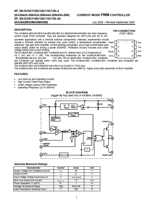
CURRENT MODE PWM CONTROLLER
July 2002 – Revised September 2005
PIN FUNCTION
N FUNCTION 1 COMP 2 VFB
3 ISENSE
4 RT/CT
5 GROUND 6 OUTPUT
is pin is the Error Amplifier output and is made for loop compensation. This is the inverting input of the Error Amplifier. It is normally connected to the switching power supply output through a resistor divider. A voltage proportional to inductor current is connected to this input. The PWM uses this information to terminate the output switch conduction. The oscillator frequency and maximum Output duty cycle are programmed by connecting resistor RT to Vref and capacitor CT to ground. This pin is the combined control circuitry and power ground. This output directly drives the gate of a power MOSFET. Peak currents up to 1A are sourced and sink by this pin. This pin is the positive supply of the integrated circuit. This is the reference output. It provides charging current for capacitor CT through resistor RT .
finFET
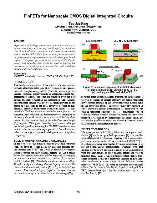
Optimization of Fin Orientation The transconductance of a FinFET is dependent on its layout orientation, due to carrier mobility anisotropy in crystalline Si [8]. The channel surfaces of a FinFET lie in the (110) crystallographic plane when the fin is oriented parallel or perpendicular to the wafer flat or notch of a standard (100) wafer. Hole mobility is enhanced, while electron mobility is degraded, for a (110) Si surface as compared with a (100) Si surface [15]. To simultaneously achieve maximum NMOS and PMOS drive currents, a (100) sidewall surface for NMOS and (110) sidewall surface for PMOS is desirable. This can be achieved by orienting the PMOS fins to be either perpendicular or parallel to the flat or notch of a (100) wafer and orienting the NMOS fins to be rotated at a 45o angle (Fig. 3). Non-Manhattan layout geometry may pose a yield issue for sub-wavelength lithography, however. An alternative approach is to use a (110) wafer to allow the optimal CMOS FinFET sidewall surface orientations to be achieved with Manhattan layouts.
RT3J33M中文资料

DESCRIPTIONRT3J33M is a composite transistor built with two INJ0003AX chips in SC-88 package.FEATURE・Input impedance is high, and not necessary to consider a drive electric current.・Vth is low, and drive by low voltage is possible. Vth=0.6~1.2V ・Low on Resistance. Ron=2Ω(TYP) ・High speed switching.・Small package for easy mounting.APPLICATIONhigh speed switching , Analog switchingPRELIMINARYRT3J33MComposite Transistor For high speed switching Silicon P-channel MOSFETMAXIMUM RATING (Ta=25℃)SYMBOL PARAMETER RATING UNIT V DSS Drain-source voltage -20 V V GSS Gate-source voltage ±8 V I D Drain current-200mA P D Total power dissipation(Ta=25℃) 150 mWT ch Channel temperature +125 ℃ T stg Range of Storage temperature-55~+125℃Switching time test conditionPRELIMINARY RT3J33MComposite Transistor For high speed switching Silicon P-channel MOSFETELECTRICAL CHARACTERISTICS (Ta=25℃)LimitsSymbol Parameter Test conditions Min Typ MaxUnitV (BR)DSS Drain-source breakdown voltage I D =-100μA, V GS =0V-20 - - V I GSS Gate-source leak current V GS =±5V, V DS =0V- - ±0.5μA I DSS Zero gate voltage drain current V DS =-20V ,V GS =0V - - -50 μA V thGate threshold voltageI D =-250μA, V DS = V GS -0.6 - -1.2V | Y fs |Forward transfer admittanceV DS =-10V, I D =-0.1A - 280 - mS R DS(ON) Static drain-source on-state resistance I D =-100mA, V GS =-4.0V-2 - Ω C iss Input capacitance V DS =-10V, V GS =0V,f=1MHz - 37 - pF C oss Output capacitance V DS =-10V, V GS =0V,f=1MHz - 12 - pF t ON - 16 - t OFF Switching timeV DD =-5V , I D =-10mA V GS =0~-5V-110-nsV input output DD =-5V D.U.≦1%Common source Ta=25℃V DS(ON )-5V 0VV DD-5V10μs 50test circuitwaveform waveformTYPICAL CHARACTERISTICSMarketing division, Marketing planning department 6-41 Tsukuba, Isahaya, Nagasaki, 854-0065 Japan。
JANSR2N7425中文资料
Pre- @ VGS = -12V, TC = 25°C Continuous Drain Current
ID @ VGS = -12V, TC = 100°C Continuous Drain Current
IDM
Pulsed Drain Current
* Current is limited by pin diameter. 2
Thermal Resistance
Parameter
RthJC RthCS RthJA
Junction-to-Case Case-to-Sink Junction-to-Ambient
Min Typ Max
— — 0.50 — 0.21 — — — 48
Units °C/W
Test Conditions Typical socket mount
Modified MOSFET symbol showing the internal inductances.
Ciss Coss Crss
Input Capacitance Output Capacitance Reverse Transfer Capacitance
— 6000 — — 1400 — pF — 400 —
Absolute Maximum Ratings
Product Summary
Part Number
BVDSS
IRHM9160
-100V
IRHM93160
-100V
RDS(on) 0.073Ω 0.073Ω
ID -35*A -35*A
Features:
n Radiation Hardened up to 3 x 10⁵ Rads (Si) n Single Event Burnout (SEB) Hardened n Single Event Gate Rupture (SEGR) Hardened n Gamma Dot (Flash X-Ray) Hardened n Neutron Tolerant n Identical Pre- and Post-Electrical Test Conditions n Repetitive Avalanche Rating n Dynamic dv/dt Rating n Simple Drive Requirements n Ease of Paralleling n Hermetically Sealed n Electrically Isolated n Ceramic Eyelets
SKY77344
APPLICATION NOTESKY77344-21 Power Amplifier Module — Evaluation InformationApplicability: SKY77344 Version -21IntroductionThis Application Note describes the functionality, board layout and applications instructions of the SKY77344-21 Power Amplifier Module. The SKY77344-21 Power Amplifier Module (PAM) is designed for quad-band cellular handsets comprising GSM850/900, DCS1800/PCS1900, and supports Class 12 General Packet Radio Service (GPRS) multi-slot operation, and Enhanced Data GSM Environment (EDGE) (8PSK) linear modulation. A single analog control voltage is used at the VRAMP port for both GMSK and EDGE modes. The active logic level at the MODE terminal determines the function of the VRAMP signal.The EDGE mode is supported with a linear open loop configuration where amplifier gain is held constant with VRAMP and output power is determined by input power. GMSK mode is supported by operating the SKY77344-21 as a variable gain amplifier where VRAMP controls gain and resultant output power.The SKY77344-21 PAM consists of an Indium Gallium Phosphide (InGaP) PA block, a BiCMOS multi-function controller (MFC) block, and impedance-matching circuitry. The new BiCMOS collector voltage amplitude controller (COVAC) provides envelope amplitude control and bias optimization for each mode of operation, thus reducing sensitivity to input drive, temperature, power supply, and process variations. Embedded within a single Gallium Arsenide (GaAs) die using InGaP technology, one Heterojunction Bipolar Transistor (HBT) PA lineup supports the GSM850/900 bands and another supports the DCS1800 and PCS1900 bands.The module also contains band select switching circuitry to select GSM (logic 0) and DCS/PCS (logic 1) as determined from the Band Select (BS) signal. As determined by the MODE control, VRAMP controls the level of output power for GMSK modulation or optimizes the performance for EDGE modulation. The Enable input signal allows initial turn-on of the PAC circuitry to minimize battery drain.Figure 1. SKY77344-21 Functional Block DiagramAPPLICATION NOTE SKY77344 POWER AMPLIFIER MODULE – EVALUATION INFORMATIONOPERATIONAL CONSIDERATIONSThe SKY77344-21 is intended for multi-modulation GSM/GPRS/EDGE handset applications. The next two sections will describe how the module should be configured for use with GSM/GPRS and the EDGE waveforms.GSM/GPRS OPERATIONFor GMSK operation, set EN input high and MODE low (< 0.5 V). Select the desired TX band by setting the BS low (CEL/EGSM) or high (DCS/PCS). VRAMP is a pulsed ramp input that controls the module output power in a manner similar to a traditional “VAPC” or “VPC” input control signal. The pulsed ramp profile is optimized with the baseband DAC control software to be compliant with PVT and ORFS due to switching system specifications.VRAMP FilterIt is advisable to use a first order RC network on VRAMP line to filter noise introduced by the baseband DAC. The filter should be designed so as to not slow down the power mask timing requirements.Recommended RC network values are: R = 110 Ω, C = 10 nF, (F POLE = 145 kHz).Depending upon the baseband DAC operating characteristics, the RC network can be redesigned or eliminated. The values selected for the RC network are critical for correct saturation detection / correction operation. A limit of R < 1 kΩ is recommended.Power Control SchemeAn integrated power control scheme is used to control the PA output power for GMSK operation. The COVAC configuration combined with a coupler / log detector provides a closed loop feedback mechanism. The COVAC scheme is based on limiting power at the collector by limiting collector voltage while the feedback path monitors output power. During saturated GMSK operation, the RF input drive is held constant while saturation characteristics of the amplifier are used to control output power. Reduction of the collector voltage of the amplifier driver stages forces saturation, effectively limiting the large signal gain and reducing the drive level to the final stage amplifier. Coincident reduction of the quiescent current in the amplifier provides reduction of the small signal gain along with reduced current drain. Significant reduction of the final stage bias point below the base-emitter voltage is required to meet aggressive low power performance as well.Table 2 is a simplified schematic of PA control scheme which senses the detected output power, compares it to the external VRAMP signal and sets the required bias voltage at the PA collector.Figure 2. SKY77344-21 Power Control Scheme – GMSK ModeSKY77344 POWER AMPLIFIER MODULE – EVALUATION INFORMATION APPLICATION NOTESaturation Detection/Correction Operation Description and External V RAMP Filter GuidelineWhen the SKY77344-21 PAM saturates under conditions of low battery and/or VSWR, a decrease in the internal power control loop gain-bandwidth occurs, producing high level switching transients on the falling edge of the burst. To prevent this condition, the SKY77344-21 includes an autonomous saturation detection / correction function. When saturation is detected, output power is reduced by approximately 0.5 dB which is sufficient to increase the loop gain-bandwidth to a level that restores switching transients to specification compliance (with additional production margin).Under some environmental conditions, the PA may enter soft saturation, which is the transition region between no saturation and hard saturation. To ensure compliant switching transients in this region, the PA is “tested” for soft saturation by pushing the PA into hard saturation. This is achieved by reducing the output power approximately 0.5 dB about 100 μs after the start of every burst. This “correct every burst” feature occurs for all V RAMP levels greater than 1.0 V. Saturation is detected during the first 100 μs or “high” part of the carrier power envelope followed by the required power reduction. Whether the PA is saturated or non-saturated, a ~0.5 dB power correction will be observed for all V RAMP levels greater than 1.0 V. Nominally, this power correction will occur ~100 μs after the start of the burst.However, as V RAMP exceeds the voltage required for nominal rated output power (~1.85 V), the correction duty cycle will increase from 100 μs / 577 μs (17%) to 100%. As the applied V RAMP is increased beyond that required for nominal rated power, the internal V RAMP, which references the internal PA control loop, must be further decreased to pull the control loop out of saturation. Since the internal pullback time constant is fixed, this action requires additional time and results in increasing the correction duty cycle. For V RAMP greater than~2.2 V, which is beyond the normal operating region of the device, the duty cycle is ~100% and the saturation detection/correction circuitry is no longer active.Under conditions of low battery and/or VSWR PA load, where the saturated PA output power (P SAT) has decreased, the correction duty cycle will also increase beyond the nominal 17%. The internal V RAMP must be decreased below the lower V RAMP @P SAT value to pull the control loop out of saturation. Since the internal pullback time constant is fixed, this action requires additional time or longer correction duty cycle. To ensure part-to-part constancy, the correction factor (~0.5 dB for Low Band, ~0.4 dB for High Band) is screened at production test.Figure 3 illustrates a block diagram of the saturation detection/correction technique used in the SKY77344-21. Depicted are the power amplifier, detector, collector voltage power control loop, and the saturation detection/correction functions, V RAMP comparator, timer, correction offset ramp generator, I OFFSET current source, and saturation detector.Figure 3. SKY77344-21 Block Diagram of Saturation Detection / Correction TechniqueAPPLICATION NOTE SKY77344 POWER AMPLIFIER MODULE – EVALUATION INFORMATION Also shown in Figure 3 are two V RAMP RC LP filters. The internal LP filter has a ~335 kHz 3 dB cutoff frequency which is adequate for suppressing DAC quarter-bit step transition transients. If courser DAC step sizes are used, an external V RAMP filter may be added for additional transient suppression. However, the values selected for R EXT and C EXT are critical for correct saturation detection / correction operation. Selection guidelines for the R EXT and C EXT values are addressed in the last section.When V RAMP exceeds ~1.0 V, an internal 100 μs timer is initiated. After the timer expires, saturation is checked followed by the power correction. The internal reference voltage applied to the power control loop integrator input (V RAMP F ILT) is reduced by subtracting a linearly increasing voltage offset from the applied V RAMP control level. This voltage offset is created by sinking a linearly increasing offset current (I OFFSET < 100 μA) across the internal and external V RAMP LP filter resistors. The V RAMP F ILT power control reference voltage decreases with time until the ~0.5 dB power reduction target is met, at which point I OFFSET is held constant until V RAMP decreases below 0.9 V or a PA enable high-to-low transition occurs. For multi-slot GMSK-to-GMSK operation, transitioning V RAMP below ~0.9 V between slots is required to reset the saturation detection/correct function for correct operation in the following slot.V OFFSET = (R EXT + R1) * I OFFSET * Delta TWhere:R EXT = external V RAMP filter resistorR1 = internal V RAMP filter resistor segment (approximately 3 kΩ).I OFFSET = linearly increasing current ramp (1.1 A per second).Delta T = V OFFSET ramp duration: Time between saturation detection and P OUT reduction completion.The V OFFSET ramp slope was optimized with the internal closed loop time constants to achieve correct saturation detection / correction operation. If R EXT is non-zero, the V OFFSET ramp slope [( R EXT + R1)* I OFFSET] is faster than the loop time constants causing P OUT to reduce beyond the ~0.5 dB design point.To maintain the P OUT reduction within a ~0.4 dB for HB to ~0.5 dB for LB window, limiting R EXT to < 1 kΩ is recommended. For a desired filter pole, the external shunt capacitor (C EXT) should be increased using the following relation.C EXT = 1/(2π * F POLE * R EXT).EDGE (8PSK) OPERATIONThe module operates in a linear open loop configuration with P OUT controlled by the input power (P IN). Output power is defined as: P OUT = P IN + GainTo operate the SKY77344-21 in EDGE (8PSK) mode, set both EN input and MODE high. Select the desired TX band by setting BS low for CEL/EGSM or high for DCS/PCS. The analog input, VRAMP, adjusts the quiescent current and is set to obtain the desired ACPR and EVM margin for the appropriate band. VRAMP is intended to remain fixed throughout the transmit slot.Using bias control, VRAMP, allows gain control and optimization of the current at lower output power; however, the bias control greatly affects the linearity of the module. Achieving the desired power while simultaneously meeting the linearity requirements necessitates careful setting of VRAMP.During the linear EDGE mode, the amplifier quiescent current must be maintained constant, independent of temperature, to maintain constant intercept performance. The disadvantage of constant bias is that the small signal gain decreases with increasing temperature. Voltage headroom on each amplifier stage must also be maintained to prevent compression and degradation of the linearity. At reduced output power levels, the quiescent bias can be reduced to minimize current drain. Analog control of the bias points is provided through the VRAMP control signal. Output power is detected and translated to DC voltage linearly relative to the output power in dB.Closed loop power control for EDGE mode is made possible with the RF power detector voltage at the VDET terminal. When the PA is disabled (EN < 0.5 V), the VDET terminal is tri-state (high impedance), allowing other 3G PAs to share a common VDET connection. A power control circuit external to the MFC can use this signal to achieve closed loop EDGE operation. Saturation Detection / Correction is disabled in EDGE operation.SKY77344 POWER AMPLIFIER MODULE – EVALUATION INFORMATION APPLICATION NOTELOGIC and INPUT SETTINGSTable 1. Control LogicOperational State EN BS MODE VRAMPoff 0 X X X Standby/PAActive 2Low band GMSK2 1Active 31Low band EDGE3 1Active 21High band GMSK2 1Active 31High band EDGE3 111X = don’t care2VRAMP controls output power3VRAMP sets PA biasTable 2. Maximum Bias Voltages to Achieve Rated POUT – EDGE and GMSKInputBand and ModulationVRAMP Mode CEL/EGSM_TX EDGE 2.0 V HighDCS/PCS_TX EDGE 2.0 V HighCEL/EGSM_TX GMSK 2.0 V LowDCS/PCS_TX GMSK 2.0 V LowSKY77344-21 Test FixtureThe SKY77344-21 test fixture assembly is shown in Figure 3 and the schematic of the test fixture is shown in Figure 4. Artwork of the fourlayers of the test fixture assembly is shown in Figure 5 through Figure 8.Not all components shown are installed on the test fixture. R1 is installed to connect VRAMP from P1. Alternately, R2 and J1 may beinstalled to allow application of VRAMP via the SMA coaxial connector. C3, C6, and C7 are not normally installed but provide mountinglocations for additional capacitance to VBATT to insure good low frequency bypassing, depending on the quality of the bench powersupply used. A VBATT_SENSE line (Figure 3, connector P1.5) provides feedback to a sensing power supply to help maintain proper voltageunder transient conditions.A single analog control voltage is used at the VRAMP port for both the GMSK and EDGE modes. The active signal is ultimately determinedby the MODE control logic level applied. Figure 11 through Figure 15 provide recommended control timing and VRAMP profiles for properoperation in GMSK mode, EDGE mode, and multimode slot-to-slot operation. Table 1 shows the proper control logic combinations forGMSK and EDGE modes of operation for low band and high band.APPLICATION NOTE SKY77344 POWER AMPLIFIER MODULE – EVALUATION INFORMATIONFigure 4. SKY77344-21 Power Amplifier Text FixtureSKY77344 POWER AMPLIFIER MODULE – EVALUATION INFORMATION APPLICATION NOTEFigure 5. Power Amplifier Test Fixture Schematic Diagram – SKY77344-21APPLICATION NOTE SKY77344 POWER AMPLIFIER MODULE – EVALUATION INFORMATIONFigure 6. SKY77344-21 Power Amplifier Test Fixture PCB Layer 1SKY77344 POWER AMPLIFIER MODULE – EVALUATION INFORMATION APPLICATION NOTEFigure 7. SKY77344-21 Power Amplifier Test Fixture PCB Layer 2APPLICATION NOTE SKY77344 POWER AMPLIFIER MODULE – EVALUATION INFORMATIONFigure 8. SKY77344-21 Power Amplifier Test Fixture PCB Layer 3Figure 9. SKY77344-21 Power Amplifier Test Fixture PCB Layer 4Figure 10. Application Circuit Diagram for SKY77344-21 Power AmplifierBattery BypassingVBATT line of the PA module requires low frequency bypassing capacitance. In modern communication systems, a GSM PA draws rapid pulses of current that can cause a significant transient during the transmission. This might affect the output power mask at high power levels. Most lab supplies are not suited for digital communications and do not emulate the phone board battery condition. Hence, in some cases a higher value capacitor of 68 μF may be required.In the phone board, battery ESR will reduce the transient voltage pulse and should not require more than a 22μF bypass capacitor. The bypass capacitor should be a good quality ceramic or tantalum capacitor.INPUT / OUTPUT PAD DESCRIPTIONFigure 11. SKY77344-21 Pad Names and Configuration (Top View)Table 3. SKY77344-21 Pad DescriptionsPad 1 Na me Description1 BS Band Select:Low = GSM850/900 TX; High = DCS1800 / PCS1900 2 ENABLE Transmit Enable / Disable: High = Enable, Low = Disable3 VRAMP GMSK Power Control / EDGE Mode Bias Control4 DCS/PCS_IN DCS1800 / PCS1900 RF Input5 GSM_IN GSM850/900 RF Input 13GSM_OUTGSM850/900 RF Output 15 DCS/PCS_OUT DCS1800 / PCS1900 RF Output 17 VBATT1 DC (Battery) Supply 18 VBATT2 DC (Battery) Supply 19 VDET RF Log Detector Output 20 MODE GMSK/EDGE Power Control Mode: Low = GMSK, High = EDGE GROUNDGROUND PADGround pad is device underside.1. Pad numbers 6-12, 14, 16 are GROUND padsFigure 12. Transmit Timing Diagram for Single-Slot GMSK OperationFigure 13. Transmit Timing Diagram for Single-Slot EDGE TimingFigure 14. Transmit Timing Diagram for Multi-slot GMSK to EDGE Slot OperationFigure 15. Transmit Timing Diagram for Multi-slot GMSK to EDGE Operation – Maximum Timing AdvanceFigure 16. Transmit Timing Diagram for Multi-slot EDGE to GMSK OperationFigure 17. Transmit Timing Diagram for Multi-slot GMSK to GMSK OperationFigure 18. Recommended RAMP ProfileGMSK Ramp Profile Recommendations•3 μs from ENABLE edge to VRAMP pedestal set (precharge) •10 μs log ramp-down profile•5 μs VRAMP pedestal set at –2 dBm (LB), –5 dBm (HB) •1.5 μs dwell at 500 mV ramp level •TX_ANT_SW_EN set at end of pedestal •VRAMP transitioned low•10 μs log ramp-up profile •ENABLE, TX_ANT_SW_EN set lowRevision HistoryRevision Date DescriptionA February 16, 2010 Initial ReleaseReferencesData Sheet: SKY77344-21 PA Module for Quad-Band GSM / EDGE, Document No. 201086Copyright © 2010 Skyworks Solutions, Inc. All Rights Reserved.Information in this document is provided in connection with Skyworks Solutions, Inc. (“Skyworks”) products or services. These materials, including the information contained herein, are provided by Skyworks as a service to its customers and may be used for informational purposes only by the customer. Skyworks assumes no responsibility for errors or omissions in these materials or the information contained herein. Skyworks may change its documentation, products, services, specifications or product descriptions at any time, without notice. Skyworks makes no commitment to update the materials or information and shall have no responsibility whatsoever for conflicts, incompatibilities, or other difficulties arising from any future changes.No license, whether express, implied, by estoppel or otherwise, is granted to any intellectual property rights by this document. Skyworks assumes no liability for any materials, products or information provided hereunder, including the sale, distribution, reproduction or use of Skyworks products, information or materials, except as may be provided in Skyworks Terms and Conditions of Sale.THE MATERIALS, PRODUCTS AND INFORMATION ARE PROVIDED “AS IS” WITHOUT WARRANTY OF ANY KIND, WHETHER EXPRESS, IMPLIED, STATUTORY, OR OTHERWISE, INCLUDING FITNESS FOR A PARTICULAR PURPOSE OR USE, MERCHANTABILITY, PERFORMANCE, QUALITY OR NON-INFRINGEMENT OF ANY INTELLECTUAL PROPERTY RIGHT; ALL SUCH WARRANTIES ARE HEREBY EXPRESSLY DISCLAIMED. SKYWORKS DOES NOT WARRANT THE ACCURACY OR COMPLETENESS OF THE INFORMATION, TEXT, GRAPHICS OR OTHER ITEMS CONTAINED WITHIN THESE MATERIALS. SKYWORKS SHALL NOT BE LIABLE FOR ANY DAMAGES, INCLUDING BUT NOT LIMITED TO ANY SPECIAL, INDIRECT, INCIDENTAL, STATUTORY, OR CONSEQUENTIAL DAMAGES, INCLUDING WITHOUT LIMITATION, LOST REVENUES OR LOST PROFITS THAT MAY RESULT FROM THE USE OF THE MATERIALS OR INFORMATION, WHETHER OR NOT THE RECIPIENT OF MATERIALS HAS BEEN ADVISED OF THE POSSIBILITY OF SUCH DAMAGE.Skyworks products are not intended for use in medical, lifesaving or life-sustaining applications, or other equipment in which the failure of the Skyworks products could lead to personal injury, death, physical or environmental damage. Skyworks customers using or selling Skyworks products for use in such applications do so at their own risk and agree to fully indemnify Skyworks for any damages resulting from such improper use or sale.Customers are responsible for their products and applications using Skyworks products, which may deviate from published specifications as a result of design defects, errors, or operation of products outside of published parameters or design specifications. Customers should include design and operating safeguards to minimize these and other risks. Skyworks assumes no liability for applications assistance, customer product design, or damage to any equipment resulting from the use of Skyworks products outside of stated published specifications or parameters. Skyworks, the Skyworks symbol, “Breakthrough Simplicity,” DCR, Helios, HIP3, Innovation to Go, Intera, iPAC, LIPA, Polar Loop, and System Smart are trademarks or registered trademarks of Skyworks Solutions, Inc., in the United States and other countries. Third-party brands and names are for identification purposes only, and are the property of their respective owners. Additional information, including relevant terms and conditions, posted at , are incorporated by reference.。
A3150光耦DataSheet
U E D P R O D U C T E F E R E N C E O N L Y .U250 f o r n e w d e s i g n Data Sheet 27621.40The A3150JLT and A3150JUA programmable switches provide tooth/valley recognition in large gear-tooth sensing applications. Each sensor consists of a single element, chopper-stabilized Hall-effect IC that can be programmed to the desired magnetic switch point, opti-mizing sensor airgap and timing accuracy performance after final packaging. The small package can be easily assembled and used in conjunction with a wide variety of gear/target shapes and sizes. The two devices differ only in package style.The sensing technology used for this sensor is Hall-effect based.The sensor incorporates a single-element Hall IC that switches inresponse to magnetic signals created by a ferrous target. The program-mability of the circuit eliminates magnet and system offsets such as those caused by tilt yet provides zero-speed detection capabilities without the associated running jitter inherent in classical digital solu-tions.A proprietary dynamic offset cancelation technique, with an internal high-frequency clock, reduces the residual offset voltage,which is normally caused by device overmolding, temperaturedependancies, and thermal stress. This technique produces devices that have an extremely stable quiescent output voltage, are immune to mechanical stress, and have precise recoverability after temperature cycling. Many problems normally associated with low-level analog signals are minimized by having the Hall element and amplifier in a single chip. Output precision is obtained by internal gain adjustments during the manufacturing process and operate-point programming in the user’s application.This sensor system is ideal for use in gathering speed, position, and timing information using gear-tooth-based configurations. TheA3150JLT/JUA are particularly suited to those applications that require accurate duty cycle control or accurate edge detection. The lower vibration sensitivity also makes these devices extremely useful for transmission speed sensing.3150Always order by complete part number: the prefix 'A' + the basic four-digit part number + a suffix to indicate operating temperature range +a suffix to indicate package style, e.g., A3150JLT .PROGRAMMABLE, CHOPPER-STABILIZED, HALL-EFFECT SWITCHContinued next page115 Northeast Cutoff, Box 15036Worcester, Massachusetts 01615-0036 (508) 853-********PROGRAMMABLE, CHOPPER-STABILIZED, PRECISION,HALL-EFFECT SWITCHCopyright © 2000, Allegro MicroSystems, Inc.Two package styles provide a magnetically opti-mized package for most applications. Suffix ‘–LT’ is a miniature SOT-89/TO-243AA transistor package for surface-mount applications; while suffix ‘–UA’ is a three-lead ultra-mini-SIP for through-hole mounting.FEATURES AND BENEFITSs Chopper Stabilized forExtremely Low Switch-Point Drift and Immunity to Mechanical Stresss Externally Programmed Switch Point s On-Chip Supply-Transient Protection s Output Short-Circuit Protections Single-Chip Sensing IC for High Reliability s Small Mechanical Size s <50µs Power-On Times Wide Operating Voltage Range s Defined Power-On State3150PROGRAMMABLE, CHOPPER-STABILIZED, PRECISION,HALL-EFFECT SWITCHLimitsCharacteristic Symbol Test ConditionsMin.Typ.Max.Units Operate PointB OPProgrammable offset range 500670850G Initial (before programming)02040G Resolution8.01114G ∆B OPV CC = 14 V, after programming, B OP ≈ 500 G-358.0+35G HysteresisB hys5.02035GNOTE: Typical data is at V CC = 5 V and T A = +25°C and is for design information only.ELECTRICAL CHARACTERISTICS over operating voltage and temperature range (unless otherwise noted).LimitsCharacteristic Symbol Test Conditions Min.Typ.Max.Units Supply Voltage V CC Operating, T J < 165°C4.25–26V Power-On State POS After programming, V CC = 0 ¡ 5 V HIGH HIGH HIGH –Low Output Voltage V OUT(SAT)I OUT = 20 mA –175400mV Output Current Limit I OUTM V OUT = 12 V 658095mA Output Leakage Current I OFF V OUT = 24 V–0.210µA Supply CurrentI CCBefore programming, output OFF – 4.07.0mA Before programming, output ON– 5.08.0mA Reverse Supply Current I RCC V RCC = -30 V ––-5.0mA Power-On Delay t on V CC > 5 V–2050µs Output Rise Time t r R L = 820 Ω, C L = 20 pF –200–ns Output Fall Time t f R L = 820 Ω, C L = 20 pF–100–ns Clock Frequency f C –340–kHz Zener Voltage V Z I ZT = 100 µA, T A = 25°C 2732–V Zener Impedancez zI ZT = 10 mA, T A = 25°C –50100ΩNOTE: Typical data is at V CC = 5 V and T A = +25°C and is for design information only.MAGNETIC CHARACTERISTICS over operating supply voltage and temperature ranges.115 Northeast Cutoff, Box 15036Worcester, Massachusetts 01615-0036 (508) 853-50003150PROGRAMMABLE, CHOPPER-STABILIZED, PRECISION,HALL-EFFECT SWITCHTYPICAL ELECTRICAL CHARACTERISTICS255075100AMBIENT TEMPERATURE IN °C-50Dwg. GH-053-2125-25S U P P L Y C U R R E N T I N m A5.04.03.02.01.015010152025SUPPLY VOLTAGE IN VOLTSDwg. GH-041-25S U P P L Y C U R R E N T I N m A10300AMBIENT TEMPERATURE IN °C200Dwg. GH-040-4S A T U R A T I O N V O L T A G E I N m V3150PROGRAMMABLE, CHOPPER-STABILIZED, PRECISION,HALL-EFFECT SWITCHFUNCTIONAL DESCRIPTIONChopper-Stabilized Technique. These devices use a proprietary dynamic offset cancellation technique, with an internal high-frequency clock to reduce the residual offset voltage of the Hall element that is normally caused by device overmolding, temperature dependencies, and thermal stress.This technique produces devices that have an extremely stable quiescent Hall output voltage, are immune to thermal stress, and have precise recoverability after temperature cycling. Thistechnique will also slightly degrade the device output repeatabil-ity.The Hall element can be considered as a resistor arraysimilar to a Wheatstone bridge. A large portion of the offset is a result of the mismatching of these resistors. The chopper-stabilizing technique cancels the mismatching of the resistors by changing the direction of the current flowing through the Hall plate and Hall voltage measurement taps, while maintaining the Hall-voltage signal that is induced by the external magnetic flux.The signal is, then, captured by a sample-and-hold circuit.Operation. The output of these devices switches low (turns ON) when a magnetic field (south pole) perpendicular to the Hall sensor exceeds the operate point threshold (B OP ). After turn-ON, the output is capable of sinking 25 mA and the output voltage is V OUT(SAT). When the magnetic field is reduced below the release point (B RP ), the device output goes high (turns OFF).The difference in the magnetic operate and release points is the hysteresis (B hys ) of the device. This built-in hysteresis allows clean switching of the output even in the presence of external mechanical vibration and electrical noise.Applications. It is strongly recommended that an external bypass capacitor be connected (in close proximity to the Hall sensor) between the supply and ground of the device to reduce both external noise and noise generated by the chopper-stabiliza-tion technique.The simplest form of magnet that will operate these devices is a bar magnet with the south-seeking pole towards the branded surface of the device. Many other methods of operation are possible. Extensive applications information on magnets and Hall-effect sensors is also available in the Allegro Electronic Data Book AMS-702 or Application Note 27701, orO U T P U T V O L T A G EFLUX DENSITYDwg. GH-007-2115 Northeast Cutoff, Box 15036Worcester, Massachusetts 01615-0036 (508) 853-50003150PROGRAMMABLE, CHOPPER-STABILIZED, PRECISION,HALL-EFFECT SWITCHPROGRAMMING PROTOCOLThe A3150JLT and A3150JUA operate points are pro-grammed by serially addressing the device through the supply terminal (pin1). After the correct operate point is determined, the device programming bits are selected and then a “lock” set to prevent any further (accidental)programming.Program Enable. To program the device, a sequence of pulses is used to activate/enable the addressing mode as shown in figure 1. This sequence of a V PP pulse, at least seven V PH pulses, and a V PP pulse with no supply interrup-tions, is designed to prevent the device from being pro-grammed accidentally (for example, as a result of noise on the supply line).VV V Dwg. WH-013Figure 1 — Program enablePROGRAMMING PROTOCOL over operating temperature range.LimitsCharacteristic Symbol DescriptionMin.Typ.Max.Units Programming VoltageV PL Minimum voltage during programming4.55.0 5.5V V PH 9.01011V V PP202325V Programming Current I PP Max. supply current during programming –250–mA Pulse Widtht d(0)OFF time between bits20––µs t d(1)Enable, address, program, or lock bit ON time 20––µs t dPProgram pulse ON time 100300–µs Pulse Rise Time t r V PL to V PH or V PP 11––µs Pulse Fall Timet fV PH or V PP to V PL 5.0––µsNOTE: Typical data is at T A = +25°C and is for design information only.3150PROGRAMMABLE, CHOPPER-STABILIZED, PRECISION,HALL-EFFECT SWITCH* In application, the terms “gear” and “target” are often interchanged. However, “gear” is preferred when motion is transferred.Address Determination. The operate point is adjust-able in 64 increments. With the appropriate target or gear*in position, the 64 switch points are sequentially selected (figure 2) until the required operate point is reached. Note that the difference between the operate point and the release point (hysteresis) is a constant for all addresses.Set-Point Programming. After the desired set-point address is determined (0 through 63), each bit of theequivalent binary address is programmed individually. For example, as illustrated in figure 3, to program address code 5 (binary 000101), bits 1 and 3 need to be programmed.Each bit is programmed during the wide V PP pulse and is not reversible.Lock Programming. After the desired set point is programmed, the program lock is then activated (figure 4)to prevent further programming of the device.V PV 0Dwg. WH-014A D D R E S S 0A D D R E S S 1A D D R E S S 2A D D R E S S N (UP T O 63)A D D R E S S N -1A D D R E S S N -2Figure 2 — Address determinationFigure 4 — Lock programmingV V VDwg. WH-016Figure 3 — Set-point programmingV V V Dwg. WH-015A115 Northeast Cutoff, Box 15036Worcester, Massachusetts 01615-0036 (508) 853-50003150PROGRAMMABLE, CHOPPER-STABILIZED, PRECISION,HALL-EFFECT SWITCHAll Allegro sensors are subjected to stringent qualification requirements prior to being released to production.To become qualified, except for the destructive ESD tests, no failures are permitted.CRITERIA FOR DEVICE QUALIFICATIONQualification Test Test Method and Test Conditions Test Length SamplesComments Biased Humidity (HAST)T A = 130°C, RH = 85%50 hrs 77V CC = V OUT = 5 V High-Temperature JESD22-A108,408 hrs77V CC = 24 V,Operating Life (HTOL)T A = 150°C, T J = 165°C V OUT = 20 V Accelerated HTOLJESD22-A108,504 hrs 77V CC = 24 V,T A = 175°C, T J = 190°C V OUT = 20 VAutoclave, Unbiased JESD22-A102, Condition C,96 hrs 77T A = 121°C, 15 psig High-Temperature MIL-STD-883, Method 1008,1000 hrs 77(Bake) Storage Life T A = 170°CTemperature CycleMIL-STD-883, Method 1010,500 cycles 77-65°C to +150°C Latch-Up—Pre/Post 6Reading Electro-Thermally—Pre/Post 6Induced Gate Leakage Reading ESD,CDF-AEC-Q100-002Pre/Post x per Test to failure,Human Body Model Reading test All leads > TBDElectrical DistributionsPer Specification—303150PROGRAMMABLE, CHOPPER-STABILIZED, PRECISION,HALL-EFFECT SWITCHSENSOR LOCATIONS(±0.005” [0.13 mm] die placement)Package Designators “UA” and "UA-TL"Although sensor location is accurate to three sigma for a particular design, product improvements may result in small changes to sensor location.Dwg. MH-008-80.030"0.76 mm NOMDwg. MH-011-9APackage Designator “LT”115 Northeast Cutoff, Box 15036Worcester, Massachusetts 01615-0036 (508) 853-50003150PROGRAMMABLE, CHOPPER-STABILIZED, PRECISION,HALL-EFFECT SWITCH0.440.35PACKAGE DESIGNATOR 'LT'(SOT-89/TO-243AA)Dimensions in Inches (for reference only)Dimensions in Millimeters (controlling dimensions)Dwg. MA-012-3 mmPads 1, 2, 3, and B — Low-Stress VersionPads 1, 2, and 3 only — Lowest Stress, But Not Self AligningNOTE: Exact body and lead configuration at vendor’s option within limits shown.Dwg. MA-012-3 inads 1, 2, 3, and B — Low-Stress Versionads 1, 2, and 3 only — Lowest Stress, But Not Self Aligning3150 PROGRAMMABLE, CHOPPER-STABILIZED, PRECISION,HALL-EFFECT SWITCH Surface-Mount Lead Form (Suffix '-TL')Dimensions in Inches (controlling dimensions)Dimensions in Millimeters (for reference only)PACKAGE DESIGNATOR 'UA'Dwg. MH-014E mm1.27BSC°Dwg. MH-014E inBSC°NOTES: 1.Tolerances on package height and width represent allowable mold offsets. Dimensions given are measured at the widest point (parting line).2.Exact body and lead configuration at vendor’s option within limits shown.3.Height does not include mold gate flash.4.Recommended minimum PWB hole diameter to clear transition area is 0.035” (0.89 mm).5.Where no tolerance is specified, dimension is nominal.115 Northeast Cutoff, Box 15036Worcester, Massachusetts 01615-0036 (508) 853-50003150PROGRAMMABLE, CHOPPER-STABILIZED, PRECISION,HALL-EFFECT SWITCHThe products described herein are manufactured under one or more of the following U.S. patents: 5,045,920; 5,264,783; 5,442,283;5,389,889; 5,581,179; 5,517,112; 5,619,137; 5,621,319; 5,650,719;5,686,894; 5,694,038; 5,729,130; 5,917,320; and other patents pending.Allegro MicroSystems, Inc. reserves the right to make, from time to time, such departures from the detail specifications as may be required to permit improvements in the performance, reliability, ormanufacturability of its products. Before placing an order, the user is cautioned to verify that the information being relied upon is current.Allegro products are not authorized for use as critical components in life-support appliances, devices, or systems without express written approval.The information included herein is believed to be accurate andreliable. However, Allegro MicroSystems, Inc. assumes no responsibil-ity for its use; nor for any infringements of patents or other rights of third parties that may result from its use.。
MOTOROLA MJW16010A 数据手册
1Designer's ™Data SheetNPN Silicon Power Transistors1 kV SWITCHMODE SeriesThese transistors are designed for high–voltage, high–speed, power switching in inductive circuits where fall time is critical. They are particularly suited for line–operated switchmode applications.Typical Applications:Features:•Switching Regulators •Collector–Emitter Voltage — V CEV = 1000 Vdc •Inverters •Fast Turn–Off Times•Solenoids 50 ns Inductive Fall Time — 100_C (Typ)•Relay Drivers 90 ns Inductive Crossover Time — 100_C (Typ)•Motor Controls 900 ns Inductive Storage Time — 100_C (Typ)•Deflection Circuits•100_C Performance Specified for:Reverse–Biased SOA with Inductive Load Switching Times with Inductive Loads Saturation Voltages Leakage Currents•Extended FBSOA Rating Using Ultra–fast Rectifiers •Extremely High RBSOA CapabilityDesigner’s Data for “Worst Case” Conditions — The Designer’s Data Sheet permits the design of most circuits entirely from the information presented. SOA Limitcurves — representing boundaries on device characteristics — are given to facilitate “worst case” design.Preferred devices are Motorola recommended choices for future use and best overall value.Designer’s and SWITCHMODE are trademarks of Motorola, Inc.MOTOROLA SEMICONDUCTOR TECHNICAL DATAOrder this documentby MJW16010A/D查询MJW16010A供应商MJW16010A2Motorola Bipolar Power Transistor Device DataELECTRICAL CHARACTERISTICS (T C = 25_C unless otherwise noted)CharacteristicSymbol Min Typ Max UnitOFF CHARACTERISTICS (1)Collector–Emitter Sustaining Voltage (T able 1)(I C = 100 mA, I B = 0)V CEO(sus)500——VdcCollector Cutoff Current(V CEV = 1000 Vdc, V BE(off) = 1.5 Vdc)(V CEV = 1000 Vdc, V BE(off) = 1.5 Vdc, T C = 100_C)I CEV——0.0030.0200.151.0mAdcCollector Cutoff Current(V CE = 1000 Vdc, R BE = 50 Ω, T C = 100_C)I CER —0.020 1.0mAdc Emitter Cutoff Current (V EB = 6 Vdc, I C = 0)I EBO—0.0050.15mAdcSECOND BREAKDOWNSecond Breakdown Collector Current with Base Forward Biased I S/bSee Figure 14a or 14bClamped Inductive SOA with Base Reverse Biased RBSOASee Figure 15ON CHARACTERISTICS (1)Collector–Emitter Saturation Voltage(I C = 5 Adc, I B = 1 Adc)(I C = 10 Adc, I B = 2 Adc)(I C = 10 Adc, I B = 2 Adc, T C = 100_C)V CE(sat)———0.250.450.600.711.5VdcBase–Emitter Saturation Voltage(I C = 10 Adc, I B = 2 Adc)(I C = 10 Adc, I B = 2 Adc, T C = 100_C)V BE(sat)—— 1.21.2 1.51.5VdcDC Current Gain(I C = 15 Adc, V CE = 5 Vdc)h FE58——DYNAMIC CHARACTERISTICSOutput Capacitance(V CB = 10 Vdc, I E = 0, f test = 1 kHz)C ob——400pFSWITCHING CHARACTERISTICSInductive Load (Table 1)Storage Time (T _t sv —9002000nsFall TimeJ = 100t fi—50250Crossover Time (I C = 10 Adc,I B1 = 1.3 Adc,V = 5 Vdc,C)t c—90300Storage Time BE(off)(T _t sv —1100—Fall TimeV CE(pk) = 400 Vdc)J = 150t fi—70—Crossover TimeC)t c—120—Resistive Load (Table 2)Delay Time t d —25100nsRise Time(I (I t r—325600Storage Time C = 10 Adc,V CC = 250 Vdc,I B1 = 1.3 Adc,B2 = 2.6 Adc,R B2 = 1.6 Ω)t s —13003000Fall TimePW = 30 µs,v 2%)t f—175400Storage Time Duty Cycle (V t s —700—Fall TimeBE(off) = 5 Vdc)t f—80—(1)Pulse T est: PW = 300 µs, Duty Cycle v 2%.MJW16010A3Motorola Bipolar Power Transistor Device DataV C E , C O L L E C T O R –E M I T T E R V O L T A G E (V O L T S )C , C A P A C I T A N C E (p F )V B E , B A S E –E M I T T E R V O L T A G E (V O L T S )V C E , C O L L E C T O R –E M I T T E R V O L T A G E (V O L T S )0.15I C , COLLECTOR CURRENT (AMPS)0.211.50.510I B , BASE CURRENT (AMPS)5210.50.20.10.15I C /I B = 10T J = 25°C0.2Figure 1. DC Current Gain I C , COLLECTOR CURRENT (AMPS)30.20.30.5125102030107Figure 2. Collector–Emitter Saturation Region0.15I C , COLLECTOR CURRENT (AMPS)0.050.3120.50.350h F E , D C C U R R E N T G A I N5V CE = 5 V351015Figure 3. Collector–Emitter Saturation Region 50.50.010.020.050.20.510250.1Figure 4. Base–Emitter Saturation RegionFigure 5. Capacitance53110 k 1V R , REVERSE VOLTAGE (VOLTS)10102 k 1008502015 AI C = 1 A T C = 25°CC ib5 AT J = 100°C–55°C25°C202312150.10.20.1I C /I B = 5T J = 25°CI C /I B = 10T J = 100°C0.510.30.2I C /I B = 10T J = 25°CI C /I B = 10T J = 100°C5 k 1 k 3 k 501002003005000.30.5252030505003000.331010 AC ob TYPICAL STATIC CHARACTERISTICSMJW16010A4Motorola Bipolar Power Transistor Device Data15001.55000t c , C R O S S O V E R T I M E (n s )t f i , C O L L E C T O R C U R R E N T F A L L T I M E (n s )I C , COLLECTOR CURRENT (AMPS)Figure 6. Storage Time Figure 7. Storage Time, S T O R A G E T I M E (n s )t s v t f i , C O L L E C T O R C U R R E N T F A L L T I M E (n s )t c , C R O S S O V E R T I M E (n s )I C , COLLECTOR CURRENT (AMPS)2357155000300020001000500100, S T O R A G E T I M E (n s )t s v 1.52001000I C , COLLECTOR CURRENT (AMPS)100050020010050101.520I C , COLLECTOR CURRENT (AMPS)I C , COLLECTOR CURRENT (AMPS)1500100050030020015100I C , COLLECTOR CURRENT (AMPS)Figure 8. Collector Current Fall Time Figure 9. Collector Current Fall TimeFigure 10. Crossover TimeFigure 11. Crossover TimeV BE(off) = 0 V5 VI C /I B1 = 5, T C = 75°C, V CE(pk) = 400 VI C /I B1 = 10, T C = 75°C, V CE(pk) = 400 V0.073000.05102357153000200010005001001.52007003000.05103002357151050020010050101.52030023571510205023571510 1.51000500300200151002050235715102 V V BE(off) = 0 V5 V2 V V BE(off) = 0 V5 V2 VV BE(off) = 0 V5 V2 VV BE(off) = 0 V5 V 2 VV BE(off) = 0 V5 V2 V TYPICAL INDUCTIVE SWITCHING CHARACTERISTICSMJW16010A5Motorola Bipolar Power Transistor Device Data+15150 Ω100 Ω100 µF MTP8P10MPF930MPF930MUR105MJE210150 Ω500 µFV off50 Ω+10MTP12N10MTP8P10R B1R B2A1 µF1 µFDrive Circuit*Tektronix AM503*P6302 or EquivalentScope — T ektronix 7403 or EquivalentT 1[L coil (I Cpk )V CCNote: Adjust V off to obtain desired V BE(off) at Point A.T 1 adjusted to obtain I C(pk)T 1+V–V 0 VA*I B*I CL T.U.T.1N4246GPV clampV CCI C(pk)V CE(pk)V CEI BI CI B1I B2V CEO(sus)L = 10 mH R B2 = ∞V CC = 20 Volts I C(pk) = 100 mAInductive Switching L = 200 µH R B2 = 0V CC = 20 VoltsR B1 selected for desired I B1RBSOA L = 200 µH R B2 = 0V CC = 20 VoltsR B1 selected for desired I B1Table 1. Inductive Load SwitchingI B 2, R E V E R S E B A S E C U R R E N T (A M P S )Figure 12. Inductive Switching Measurements Figure 13. Peak Reverse Base CurrentV BE(off), REVERSE BASE VOLTAGE (VOLTS)010876I B1 = 2 A1235I C = 10 A T C = 25°Ct fi t rvt, TIMEI C 90% I B1I C(pk)V CE(pk)90% V CE(pk)90% I C(pk)10% V CE(pk)10%I C(pk)2% I CI Bt svt tit cV CE 94352141 At d and t rt s and t fH.P. 214OR EQUIV.P.G.50R B = 8.5 Ω*I B*I CT.U.T.R L V CCV in0 V≈ 11 Vt r ≤ 15 ns*Tektronix AM503*P6302 or EquivalentV CC250 Vdc R L 25 ΩI C10 A I B1.3 A+15150 Ω100 Ω100 µF MTP8P10MPF930MPF930MUR105MJE210150 Ω500 µFV off50 Ω+10 V MTP12N10MTP8P10R B1R B2A1 µF1 µF T.U.T.*I C*I BAR LV CCV (off) adjusted to give specified off driveV CC 250 V I C 10 A I B1 1.3 A I B2Per Spec R B111.5 ΩR B2Per Spec R L25 ΩTable 2. Resistive Load SwitchingMJW16010A6Motorola Bipolar Power Transistor Device Data300.031051100.50.20.10.0510010003200.3Figure 14. Maximum Rated Forward BiasedSafe Operating Area1V CE , COLLECTOR–EMITTER VOLTAGE (VOLTS)BONDING WIRE LIMIT THERMAL LIMITSECOND BREAKDOWN LIMITREGION II —EXPANDED FBSOA USING MUR8100 ULTRA–FAST RECTIFIER, SEE FIGURE 17T C = 25°Cdc20V CE , COLLECTOR–EMITTER VOLTAGE (VOLTS)010001612840200400Figure 15. Maximum Reverse BiasedSafe Operating AreaI C /I B1 ≥ 4T J ≤ 100°CP O W E R D E R A T I N G F A C T O R (%)1000T C , CASE TEMPERATURE (°C)402008060402080120160Figure 16. Power Derating600800V BE(off) = 0 VV BE(off) = 5 VSECOND BREAKDOWN DERATINGTHERMAL DERATINGI C , C O L L E C T O R C U R R E N T (A M P S )I C , C O L L E C T O R C U R R E N T (A M P S )100ns II10µs1msGUARANTEED OPERATING AREA INFORMATIONFigure 17. Switching Safe Operating Area+15150 Ω100 µF MTP8P10MPF930MPF930MUR105MJE210150 Ω500 µFV off50 Ω+10MTP12N10R B1R B21 µF1 µF100 ΩMTP8P10MUR105MUR1100T.U.T.MUR8100V CE (1000 V MAX)10 µF10 mHNote: Test Circuit for Ultra–fast FBSOA Note: R B2 = 0 and V Off = –5 VoltsMJW16010A7Motorola Bipolar Power Transistor Device Datat, TIME (ms)10.010.010.70.20.10.050.02r (t ), E F F E C T I V E T R A N S I E N T T H E R M A L 0.05125102050100200500R θJC (t) = r(t) R θJC R θJC = 1 or 0.92°CWT J(pk) – T C = P (pk) R θJC (t)P (pk)t 1t 2DUTY CYCLE, D = t 1/t 2D = 0.50.20.030.02SINGLE PULSE 0.10.10.50.2R E S I S T A N C E (N O R M A L I Z E D )1000Figure 18. Thermal Response0.50.30.070.030.030.33303000.02SAFE OPERATING AREA INFORMATIONFORWARD BIASThere are two limitations on the power handling ability of a transistor: average junction temperature and second break-down. Safe operating area curves indicate I C – V CE limits of the transistor that must be observed for reliable operation;i.e., the transistor must not be subjected to greater dissipa-tion than the curves indicate.The data of Figures 14a and 14b is based on T C = 25_C;T J(pk) is variable depending on power level. Second break-down pulse limits are valid for duty cycles to 10% but must be derated when T C ≥ 25_C. Second breakdown limitations do not derate the same as thermal limitations. Allowable current at the voltages shown on Figures 14a and 14b may be found at any case temperature by using the appropriate curve on Figure 16.T J(pk) may be calculated from the data in Figure 18. At high case temperatures, thermal limitations will reduce the power that can be handled to values less than the limitations im-posed by second breakdown.REVERSE BIASFor inductive loads, high voltage and high current must be sustained simultaneously during turn–off, in most cases, with the base–to–emitter junction reverse biased. Under these conditions the collector voltage must be held to a safe level at or below a specific value of collector current. This can be accomplished by several means such as active clamping,RC snubbing, load line shaping, etc. The safe level for these devices is specified as Reverse Biased Safe Operating Area and represents the voltage–current condition allowable dur-ing reverse biased turn–off. This rating is verified under clamped conditions so that the device is never subjected to an avalanche mode. Figure 15 gives the RBSOA character-istics.SWITCHMODE DESIGN CONSIDERA TIONS1. FBSOA —Allowable dc power dissipation in bipolar power transistors decreases dramatically with increasing collector–emittervoltage. A transistor which safely dissipates 100 watts at 10 volts will typically dissipate less than 10 watts at its rated V CEO(sus). From a power handling point of view, current and voltage are not interchangeable (see Application Note AN875).2. TURN–ON —Safe turn–on load line excursions are bounded by pulsed FBSOA curves. The 10 µs curve applies for resistive loads,most capacitive loads, and inductive loads that are clamped by standard or fast recovery rectifiers. Similarly, the 100 ns curve applies to inductive loads which are clamped by ultra–fast recovery rectifiers, and are valid for turn–on crossover times less than 100 ns (see Application Note AN952).At voltages above 75% of V CEO(sus), it is essential to pro-vide the transistor with an adequate amount of base drive VERY RAPIDLY at turn–on. More specifically, safe operation according to the curves is dependent upon base current rise time being less than collector current rise time. As a general rule, a base drive compliance voltage in excess of 10 volts is required to meet this condition (see Application Note AN875).3. TURN–OFF —A bipolar transistor’s ability to withstand turn–off stress is dependent upon its forward base drive. Gross overdrive vio-lates the RBSOA curve and risks transistor failure. For this reason, circuits which use fixed base drive are often more likely to fail at light loads due to heavy overdrive (see Ap-plication Note AN875).4. OPERATION ABOVE V CEO(sus) —When bipolars are operated above collector–emitter breakdown, base drive is crucial. A rapid application of ade-quate forward base current is needed for safe turn–on, as is a stiff negative bias needed for safe turn–off. Any hiccup in the base–drive circuitry that even momentarily violates either of these conditions will likely cause the transistor to fail.Therefore, it is important to design the driver so that its out-put is negative in the absence of anything but a clean crisp input signal (see Application Note AN952).MJW16010A8Motorola Bipolar Power Transistor Device DataSWITCHMODE III DESIGN CONSIDERATIONS (Cont.)5. RBSOA —Reverse Biased Safe Operating Area has a first order de-pendency on circuit configuration and drive parameters. The RBSOA curves in this data sheet are valid only for the condi-tions specified. For a comparison of RBSOA results in sever-al types of circuits (see Application Note AN951).6. DESIGN SAMPLES —Transistor parameters tend to vary much more from wafer lot to wafer lot, over long periods of time, than from one de-vice to the next in the same wafer lot. For design evaluation it is advisable to use transistors from several different date codes.7. BAKER CLAMPS —Many unanticipated pitfalls can be avoided by using Baker Clamps. MUR105 and MUR1100 diodes are recommended for base drives less than 1 amp. Similarly, MUR405 and MUR4100 types are well–suited for higher drive require-ments (see Article Reprint AR131).MJW16010A9Motorola Bipolar Power Transistor Device DataPACKAGE DIMENSIONSCASE 340F–03ISSUE EDIM A MIN MAX MIN MAX INCHES 20.4020.900.8030.823MILLIMETERS B 15.4415.950.6080.628C 4.70 5.210.1850.205D 1.09 1.300.0430.051E 1.50 1.630.0590.064F 1.80 2.180.0710.086G 5.45 BSC 0.215 BSC H 2.56 2.870.1010.113J 0.480.680.0190.027K 15.5716.080.6130.633L 7.267.500.2860.295P 3.10 3.380.1220.133Q 3.50 3.700.1380.145R 3.30 3.800.1300.150U 5.30 BSC 0.209 BSC V3.05 3.400.1200.134NOTES:1.DIMENSIONING AND TOLERANCING PER ANSI Y14.5M, 1982.2.CONTROLLING DIMENSION: MILLIMETER.STYLE 3:PIN 1.BASE2.COLLECTOR3.EMITTER4.COLLECTORRPAKV F DGULE0.25 (0.010)MT B M0.25 (0.010)MY QSJHC4123–T––B––Y––Q–MJW16010A10Motorola Bipolar Power Transistor Device DataHow to reach us:USA /EUROPE : Motorola Literature Distribution;JAPAN : Nippon Motorola Ltd.; T atsumi–SPD–JLDC, T oshikatsu Otsuki,P .O. Box 20912; Phoenix, Arizona 85036. 1–800–441–24476F Seibu–Butsuryu–Center, 3–14–2 T atsumi Koto–Ku, T okyo 135, Japan. 03–3521–8315MFAX :****************–TOUCHTONE(602)244–6609HONG KONG : Motorola Semiconductors H.K. Ltd.; 8B T ai Ping Industrial Park, INTERNET : http://Design–NET .com51 Ting Kok Road, T ai Po, N.T ., Hong Kong. 852–26629298◊。
- 1、下载文档前请自行甄别文档内容的完整性,平台不提供额外的编辑、内容补充、找答案等附加服务。
- 2、"仅部分预览"的文档,不可在线预览部分如存在完整性等问题,可反馈申请退款(可完整预览的文档不适用该条件!)。
- 3、如文档侵犯您的权益,请联系客服反馈,我们会尽快为您处理(人工客服工作时间:9:00-18:30)。
December 2010,Volume 4,No.12(Serial No.37) Journal of Energy and Power Engineering,ISSN 1 934—8975,USA
Hard Switching Process Optimization for Selected Transistor Suited for High Power and High Frequency Operation
M.Frivaldsk ̄,P.Drgofia and P.Sphnik Department ofMechatronics andElectronics,Faculty ofElectricalEngineering,University ofZilina,Univerzitna J,Zilina 0102 ̄ Slovakia
Received:May 12,2010/Accepted:August 12,2010/Published:December 31,2010
N
Abstract:This paper deals with optimization of hard switching commutation mode for high-power.high-frequency consumer applications for selected power transistor.11he experimental investigation of suitable settings is outgoing from simulation analysis of hard switching for diferent transistor structures.For these purposes,the simulation models ofpower semiconductor switches with high level of validity have been used.After that.the experimental analysis for selected transistor was done with change of parameters that are influencing commutation process of transistor.Target of such kind of analysis was to reach as low switching losses as possible. achieving high power density and efficiency of power system,without utilization of improved switching techniques such as resonant switching.The results confirm that this task is realizable through use ofprogressive semiconductor devices such as SiC diodes and/or through latest families of M0SFET devices.
Key words:Transistor,commutation,losses,frequency,simulation,experimental analysis,converter 1.Introduction Current tendencies in the field of power electronic devices could be characterized by continuous improvement of electrical,mechanical,economical and ecological parameters.If we take into account physical phenomenon relative to mentioned requirements,then approaching the aims is possible by increasing of switching frequency along with elimination of power losses.Naturally by increasing of switching frequency generation ofhigher power loss comes to be significant. Instead of turn—on and turn—ofjF 1osses.also conduction losses are very important in high—frequency high-power applications.Nowadays a huge amount of effort is produced to find the ways how to totally eliminate almost all of the losses in power semiconductor devices 【1,2].One way is to utilize soft—switching,second way
Corresponding author:M.Frivaldsk ̄,Ph.D.,research field: power systems.E-mail:micha1.frivaldsky@fe1.uniza.sk.
1s to utilize the progressive semiconductor structures. The goal ofevery power semiconductor system design is approach to the highest efficiency with respect to maximum output power.DC/DC power supplies encounter the power levels,somewhere from a few watts for battery-operated portable equipment,several hundred to several kilo-watts for home entertainment, computer and office equipment. Synchronous rectification is also becoming popular method to improve(Switched-Mode Power Supplies)SMPS efficiency.Motor drives can use from a tenth ofa Watt to few mega Watts【3,4].Almost all the SMPS are nowadays being developed in cooperation with a power factor control O'FC)input stage in order to meet the international regulatory standards for harmonic content. The negative feedbacks of such technical improvement are additional switching losses that are generated during commutation process of mentioned boost diode and power transistor.Therefore this system needs perfect Hard Switching Process Optimization for Selected Transistor Suited for High Power and High Frequency 37 Operation
specification of suitable components for given application(boost diode,MOSFET or IGBT transistor) that is by reason of optimalization of output power and also financial costs[5]. In next chapters the investigation of hard switching commutation mode of power transistor will be solved, targeting high power density and efficiency of power system. 2.Simulation Analysis For proper selection of power semiconductor device for HF/HP application we decide to investigate three types of power transistors. It can be seen that for investigation we assigned two generations of unipolar MoSFET transistors (fylnfineon),whose RDs(ON)is minimized due to improvements in technology process.IGBT structure is selected for competition,whereby we’ve tried to find the fastest structure in current market.IGBT structure generally has beRer performance in conduction mode, but on the other side MOSFETs are faster in turn.off process.Target of this chapter is to compare and evaluate processes which are occurring during switching of transistor by utilization of simulation program fOreAD 1 5.7 Pspice).Tl1e results from simulation have been serving at selection of proper structure that was consequentially given into experimental analysis. Table1 lnvesligatedh.ansjstorsand恤eirbasicparameters. Because every commutation technique requests specific behavior of main circuit,the simulation analysis was adapted to requirement of realness and authenticity of experimental testing circuit.Simulation has been realized at constant supply voltage(325 V), what is corresponding to the maximum value of rectified voltage from 1-phase supply network.The load is represented by resistive—inductive alternative,at which maximum load current was 1 0 A.Gate resistor of transistor was set to 33 Q at which pulse front steepness of transistor’S current was di/dt=250 A/us. As we were considering high—frequency application, the simulation analysis was done at switching frequency of 1 00 kHz.The schematic of simulation testing circuit is shown on Fig.1.