MM74HCT00MTCX,MM74HCT00MX,规格书,Datasheet 资料
74HC系列芯片型号与功能介绍

电子元件知识-74系列芯片功能略表74HC01 2输入四与非门 (oc)74HC02 2输入四或非门74HC03 2输入四与非门 (oc)74HC04 六倒相器74HC05六倒相器(oc)74HC06 六高压输出反相缓冲器/驱动器(oc,30v) 74HC07 六高压输出缓冲器/驱动器(oc,30v)74HC08 2输入四与门74HC09 2输入四与门(oc)74HC10 3输入三与非门74HC11 3输入三与门74HC12 3输入三与非门 (oc)74HC13 4输入双与非门 (斯密特触发)74HC14 六倒相器(斯密特触发)74HC15 3输入三与门 (oc)74HC16 六高压输出反相缓冲器/驱动器(oc,15v) 74HC17 六高压输出缓冲器/驱动器(oc,15v)74HC18 4输入双与非门 (斯密特触发)74HC19 六倒相器(斯密特触发)74HC20 4输入双与非门74HC21 4输入双与门74HC22 4输入双与非门(oc)74HC23 双可扩展的输入或非门74HC24 2输入四与非门(斯密特触发)74HC25 4输入双或非门(有选通)74HC26 2输入四高电平接口与非缓冲器(oc,15v) 74HC27 3输入三或非门74HC28 2输入四或非缓冲器74HC30 8输入与非门74HC31 延迟电路74HC32 2输入四或门74HC33 2输入四或非缓冲器(集电极开路输出) 74HC34 六缓冲器74HC35 六缓冲器(oc)74HC36 2输入四或非门(有选通)74HC37 2输入四与非缓冲器74HC38 2输入四或非缓冲器(集电极开路输出) 74HC39 2输入四或非缓冲器(集电极开路输出) 74HC40 4输入双与非缓冲器74HC41 bcd-十进制计数器74HC42 4线-10线译码器(bcd输入)74HC43 4线-10线译码器(余3码输入)74HC44 4线-10线译码器(余3葛莱码输入)74HC45 bcd-十进制译码器/驱动器74HC46 bcd-七段译码器/驱动器74HC47 bcd-七段译码器/驱动器74HC48 bcd-七段译码器/驱动器74HC49 bcd-七段译码器/驱动器(oc)74HC50 双二路2-2输入与或非门(一门可扩展)74HC51 双二路2-2输入与或非门74HC51 二路3-3输入,二路2-2输入与或非门74HC52 四路2-3-2-2输入与或门(可扩展)74HC53 四路2-2-2-2输入与或非门(可扩展)74HC53 四路2-2-3-2输入与或非门(可扩展)74HC54 四路2-2-2-2输入与或非门74HC54 四路2-3-3-2输入与或非门74HC54 四路2-2-3-2输入与或非门74HC55 二路4-4输入与或非门(可扩展)74HC60 双四输入与扩展74HC61 三3输入与扩展74HC62 四路2-3-3-2输入与或扩展器74HC63 六电流读出接口门74HC64 四路4-2-3-2输入与或非门74HC65 四路4-2-3-2输入与或非门(oc)74HC70 与门输入上升沿jk触发器74HC71 与输入r-s主从触发器74HC72 与门输入主从jk触发器74HC73 双j-k触发器(带清除端)74HC74 正沿触发双d型触发器(带预置端和清除端)74HC75 4位双稳锁存器74HC76 双j-k触发器(带预置端和清除端)74HC77 4位双稳态锁存器74HC78 双j-k触发器(带预置端,公共清除端和公共时钟端) 74HC80 门控全加器74HC81 16位随机存取存储器74HC82 2位二进制全加器(快速进位)74HC83 4位二进制全加器(快速进位)74HC84 16位随机存取存储器74HC85 4位数字比较器74HC86 2输入四异或门74HC87 四位二进制原码/反码/oi单元74HC89 64位读/写存储器74HC90 十进制计数器74HC91 八位移位寄存器74HC92 12分频计数器(2分频和6分频)74HC93 4位二进制计数器74HC94 4位移位寄存器(异步)74HC95 4位移位寄存器(并行io)74HC96 5位移位寄存器74HC97 六位同步二进制比率乘法器74HC100 八位双稳锁存器74HC103 负沿触发双j-k主从触发器(带清除端)74HC106 负沿触发双j-k主从触发器(带预置,清除,时钟) 74HC107 双j-k主从触发器(带清除端)74HC108 双j-k主从触发器(带预置,清除,时钟)74HC109 双j-k触发器(带置位,清除,正触发)74HC110 与门输入j-k主从触发器(带锁定)74HC111 双j-k主从触发器(带数据锁定)74HC112 负沿触发双j-k触发器(带预置端和清除端)74HC113 负沿触发双j-k触发器(带预置端)74HC114 双j-k触发器(带预置端,共清除端和时钟端)74HC116 双四位锁存器74HC120 双脉冲同步器/驱动器74HC121 单稳态触发器(施密特触发)74HC122 可再触发单稳态多谐振荡器(带清除端)74HC123 可再触发双单稳多谐振荡器74HC125 四总线缓冲门(三态输出)74HC126 四总线缓冲门(三态输出)74HC128 2输入四或非线驱动器74HC131 3-8译码器74HC132 2输入四与非门(斯密特触发)74HC133 13输入端与非门74HC134 12输入端与门(三态输出)74HC135 四异或/异或非门74HC136 2输入四异或门(oc)74HC137 八选1锁存译码器/多路转换器74HC138 3-8线译码器/多路转换器74HC139 双2-4线译码器/多路转换器74HC140 双4输入与非线驱动器74HC141 bcd-十进制译码器/驱动器74HC142 计数器/锁存器/译码器/驱动器74HC145 4-10译码器/驱动器74HC147 10线-4线优先编码器74HC148 8线-3线八进制优先编码器74HC150 16选1数据选择器(反补输出)74HC151 8选1数据选择器(互补输出)74HC152 8选1数据选择器多路开关74HC153 双4选1数据选择器/多路选择器74HC154 4线-16线译码器74HC155 双2-4译码器/分配器(图腾柱输出)74HC156 双2-4译码器/分配器(集电极开路输出)74HC157 四2选1数据选择器/多路选择器74HC158 四2选1数据选择器(反相输出)74HC160 可预置bcd计数器(异步清除)74HC161 可预置四位二进制计数器(并清除异步)74HC162 可预置bcd计数器(异步清除)74HC163 可预置四位二进制计数器(并清除异步)74HC164 8位并行输出串行移位寄存器74HC165 并行输入8位移位寄存器(补码输出)74HC166 8位移位寄存器74HC167 同步十进制比率乘法器74HC168 4位加/减同步计数器(十进制)74HC169 同步二进制可逆计数器74HC170 4*4寄存器堆74HC171 四d触发器(带清除端)74HC172 16位寄存器堆74HC173 4位d型寄存器(带清除端)74HC174 六d触发器74HC175 四d触发器74HC176 十进制可预置计数器74HC177 2-8-16进制可预置计数器74HC178 四位通用移位寄存器74HC179 四位通用移位寄存器74HC180 九位奇偶产生/校验器74HC181 算术逻辑单元/功能发生器74HC182 先行进位发生器74HC183 双保留进位全加器74HC184 bcd-二进制转换器74HC185 二进制-bcd转换器74HC190 同步可逆计数器(bcd,二进制)74HC191 同步可逆计数器(bcd,二进制)74HC192 同步可逆计数器(bcd,二进制)74HC193 同步可逆计数器(bcd,二进制)74HC199 八位移位寄存器74HC210 2-5-10进制计数器74HC213 2-n-10可变进制计数器74HC221 双单稳触发器74HC230 八3态总线驱动器74HC231 八3态总线反向驱动器74HC240 八缓冲器/线驱动器/线接收器(反码三态输出) 74HC241 八缓冲器/线驱动器/线接收器(原码三态输出) 74HC242 八缓冲器/线驱动器/线接收器74HC243 4同相三态总线收发器74HC244 八缓冲器/线驱动器/线接收器74HC245 八双向总线收发器74HC246 4线-七段译码/驱动器(30v)74HC247 4线-七段译码/驱动器(15v)74HC248 4线-七段译码/驱动器74HC249 4线-七段译码/驱动器74HC251 8选1数据选择器(三态输出)74HC253 双四选1数据选择器(三态输出)74HC256 双四位可寻址锁存器74HC257 四2选1数据选择器(三态输出)74HC258 四2选1数据选择器(反码三态输出)74HC259 8为可寻址锁存器74HC260 双5输入或非门74HC261 4*2并行二进制乘法器74HC265 四互补输出元件74HC266 2输入四异或非门(oc)74HC270 2048位rom (512位四字节,oc)74HC271 2048位rom (256位八字节,oc)74HC273 八d触发器74HC274 4*4并行二进制乘法器74HC275 七位片式华莱士树乘法器74HC276 四jk触发器74HC278 四位可级联优先寄存器74HC279 四s-r锁存器74HC280 9位奇数/偶数奇偶发生器/较验器74HC28174HC283 4位二进制全加器74HC290 十进制计数器74HC291 32位可编程模74HC293 4位二进制计数器74HC294 16位可编程模74HC295 四位双向通用移位寄存器74HC298 四-2输入多路转换器(带选通)74HC299 八位通用移位寄存器(三态输出)74HC348 8-3线优先编码器(三态输出)74HC352 双四选1数据选择器/多路转换器74HC353 双4-1线数据选择器(三态输出)74HC354 8输入端多路转换器/数据选择器/寄存器,三态补码输出74HC355 8输入端多路转换器/数据选择器/寄存器,三态补码输出74HC356 8输入端多路转换器/数据选择器/寄存器,三态补码输出74HC357 8输入端多路转换器/数据选择器/寄存器,三态补码输出74HC365 6总线驱动器74HC366 六反向三态缓冲器/线驱动器74HC367 六同向三态缓冲器/线驱动器74HC368 六反向三态缓冲器/线驱动器74HC373 八d锁存器74HC374 八d触发器(三态同相)74HC375 4位双稳态锁存器74HC377 带使能的八d触发器74HC378 六d触发器74HC379 四d触发器74HC381 算术逻辑单元/函数发生器74HC382 算术逻辑单元/函数发生器74HC384 8位*1位补码乘法器74HC385 四串行加法器/乘法器74HC386 2输入四异或门74HC390 双十进制计数器74HC391 双四位二进制计数器74HC395 4位通用移位寄存器74HC396 八位存储寄存器74HC398 四2输入端多路开关(双路输出)74HC399 四-2输入多路转换器(带选通)74HC422 单稳态触发器74HC423 双单稳态触发器74HC440 四3方向总线收发器,集电极开路74HC441 四3方向总线收发器,集电极开路74HC442 四3方向总线收发器,三态输出74HC443 四3方向总线收发器,三态输出74HC444 四3方向总线收发器,三态输出74HC445 bcd-十进制译码器/驱动器,三态输出74HC446 有方向控制的双总线收发器74HC448 四3方向总线收发器,三态输出74HC449 有方向控制的双总线收发器74HC465 八三态线缓冲器74HC466 八三态线反向缓冲器74HC467 八三态线缓冲器74HC468 八三态线反向缓冲器74HC490 双十进制计数器74HC540 八位三态总线缓冲器(反向)74HC541 八位三态总线缓冲器74HC589 有输入锁存的并入串出移位寄存器74HC590 带输出寄存器的8位二进制计数器74HC591 带输出寄存器的8位二进制计数器74HC592 带输出寄存器的8位二进制计数器74HC593 带输出寄存器的8位二进制计数器74HC594 带输出锁存的8位串入并出移位寄存器74HC595 8位输出锁存移位寄存器74HC596 带输出锁存的8位串入并出移位寄存器74HC597 8位输出锁存移位寄存器74HC598 带输入锁存的并入串出移位寄存器74HC599 带输出锁存的8位串入并出移位寄存器74HC604 双8位锁存器74HC605 双8位锁存器74HC606 双8位锁存器74HC607 双8位锁存器74HC620 8位三态总线发送接收器(反相)74HC621 8位总线收发器74HC622 8位总线收发器74HC623 8位总线收发器74HC640 反相总线收发器(三态输出)74HC641 同相8总线收发器,集电极开路74HC642 同相8总线收发器,集电极开路74HC643 8位三态总线发送接收器74HC644 真值反相8总线收发器,集电极开路74HC645 三态同相8总线收发器74HC646 八位总线收发器,寄存器74HC647 八位总线收发器,寄存器74HC648 八位总线收发器,寄存器74HC649 八位总线收发器,寄存器74HC651 三态反相8总线收发器74HC652 三态反相8总线收发器74HC653 反相8总线收发器,集电极开路74HC654 同相8总线收发器,集电极开路74HC668 4位同步加/减十进制计数器74HC669 带先行进位的4位同步二进制可逆计数器74HC670 4*4寄存器堆(三态)74HC671 带输出寄存的四位并入并出移位寄存器74HC672 带输出寄存的四位并入并出移位寄存器74HC673 16位并行输出存储器,16位串入串出移位寄存器74HC674 16位并行输入串行输出移位寄存器74HC681 4位并行二进制累加器74HC682 8位数值比较器(图腾柱输出)74HC683 8位数值比较器(集电极开路)74HC684 8位数值比较器(图腾柱输出)74HC685 8位数值比较器(集电极开路)74HC686 8位数值比较器(图腾柱输出)74HC687 8位数值比较器(集电极开路)74HC688 8位数字比较器(oc输出)74HC689 8位数字比较器74HC690 同步十进制计数器/寄存器(带数选,三态输出,直接清除。
74HC00中文资料_数据手册_参数
IO = −20 µA
2.0
IO = −20 µA
4.5
IO = −20 µA
6.0
IO = −4.0 mA
4.5
IO = −5.2 mA
6.0
VOL
LOW-level output voltage VI = VIH or VIL
IO = 20 µA
2.0
IO = 20 µA
4.5
IO = 20 µA
RECOMMENDED OPERATING CONDITIONS
SYMBOL
PARAMETER
VCC VI VO Tamb
supply voltage input voltage output voltage operating ambient temperature
tr, tf
input rise and fall times
74HC00; 74HCT00
handbook, halfpage
1B 2
1A VCC 1 14
13 4B
1Y 3
12 4A
2A 4 2B 5
GND(1)
11 4Y 10 3B
2Y 6 78
Top view GND 3Y
9 3A
MNA950
handbook, halfpage A B
Y
MNA211
(1) The die substrate is attached to this pad using conductive die attach material. It can not be used as a supply pin or input.
6.0
IO = 4.0 mA
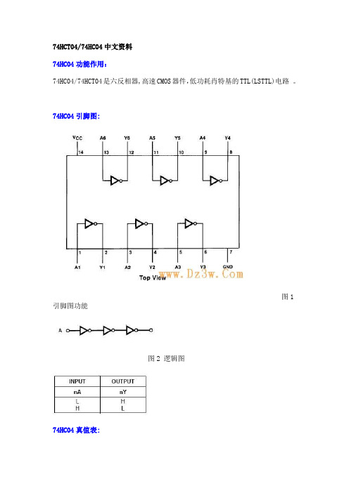
74HCT0474HC04中文资料
4.2
3.98
3.84
3.7VΒιβλιοθήκη 6.0V5.75.48
5.34
5.2
VOL
输出低电平电压
VIN=VIH 丨IOUT丨≤20 μA
2.0V
0
0.1
0.1
0.1
V
4.5V
0
0.1
0.1
0.1
6.0V
0
0.1
0.1
0.1
VIN=VIH 丨IOUT丨≤4.0 mA 丨IOUT丨≤5.2 mA
4.5V
0.2
0.26
0.33
0.4
V
6.0V
0.2
0.26
0.33
0.4
IIN
最大输入电流
VIN=VCC or GND
6.0V
±0.1
±1.0
±1.0
μA
ICC
电源电流
VIN=VCC or GND IOUT=0 μA
6.0V
2.0
20
40
μA
交流电气特性:
Symbol 符号
Parameter 参数
条件
典型
Guaranteed Limit 保证极限
4.2
4.2
4.2
VIL
输入低电平电压
2.0V
0.5
0.5
0.5
V
4.5V
1.35
1.35
1.35
6.0V
1.8
1.8
1.8
VOH
输出高电平电压
VIN=VIL 丨IOUT丨≤20 μA
2.0V
2.0
1.9
1.9
1.9
V
74VHC14MTCX,74VHC14MX,74VHC14MTC,74VHC14M,规格书,Datasheet 资料

74VHC14Hex Schmitt InverterGeneral DescriptionThe VHC14 is an advanced high speed CMOS Hex Schmitt Inverter fabricated with silicon gate CMOS technol-ogy. It achieves the high speed operation similar to equiva-lent Bipolar Schottky TTL while maintaining the CMOS low power dissipation. Pin configuration and function are the same as the VHC04 but the inputs have hysteresis between the positive-going and negative-going input thresholds, which are capable of transforming slowly changing input signals into sharply defined, jitter-free out-put signals, thus providing greater noise margin than con-ventional inverters.An input protection circuit ensures that 0V to 7V can be applied to the input pins without regard to the supply volt-age. This device can be used to interface 5V to 3V systems and two supply systems such as battery back up. This cir-cuit prevents device destruction due to mismatched supply and input voltages.Features■High Speed: t PD= 5.5 ns (typ) at V CC= 5V■Low power dissipation: I CC= 2 μA (Max) at T A= 25°C ■High noise immunity: V NIH= V NIL= 28% V CC (Min)■Power down protection is provided on all inputs■Low noise: V OLP= 0.8V (Max)■Pin and function compatible with 74HC14Ordering Code:Order Number PackageNumberPackage Description74VHC14M(Note 1)M14A14-Lead Small Outline Integrated Circuit (SOIC), JEDEC MS-012, 0.150" Narrow74VHC14MX_NL (Note 2)M14A Pb-Free 14-Lead Small Outline Integrated Circuit (SOIC), JEDEC MS-012, 0.150"Narrow74VHC14SJ(Note 1)M14D Pb-Free 14-Lead Small Outline Package (SOP), EIAJ TYPE II, 5.3mm Wide74VHC14MTC(Note 1)MTC1414-Lead Thin Shrink Small Outline Package (TSSOP), JEDEC MO-153, 4.4mm Wide74VHC14MTC_NL (Note 3)MTC14Pb-Free 14-Lead Thin Shrink Small Outline Package (TSSOP), JEDEC MO-153,4.4mm Wide74VHC14MTCX_NL (Note 2)MTC14Pb-Free 14-Lead Thin Shrink Small Outline Package (TSSOP), JEDEC MO-153,4.4mm Wide74VHC14N(Obsolete)N14A14-Lead Plastic Dual-In-Line Package (PDIP), JEDEC MS-001, 0.300" WidePb-Free package per JEDEC J-STD-020B.Note 1: Surface mount packages are also available on Tape and Reel. Specify by appending the suffix letter “X” to the ordering code.Note 2: “_NL” indicates Pb-Free product (per JEDEC J-STD-020B). Device is available in Tape and Reel only.Note 3: “_NL” indicates Pb-Free product (per JEDEC J-STD-020B).© 2010 Fairchild Semiconductor Corporation Logic Symbol/sIEEE/IECPin DescriptionsPin Names DescriptionA n InputsO n OutputsConnection Diagram/sTruth Table/sA OL HH L2Absolute Maximum Ratings(Note 4)Supply Voltage (V CC)−0.5V to +7.0V DC Input Voltage (V IN)−0.5V to +7.0V DC Output Voltage (V OUT)−0.5V to V CC+ 0.5V Input Diode Current (I IK)−20 mA Output Diode Current (I OK)±20 mA DC Output Current (I OUT)±25 mA DC V CC/GND Current (I CC)±50 mA Storage Temperature (T STG)−65°C to +150°C Lead Temperature (T L)Soldering (10 seconds)260°C Recommended Operating Conditions (Note 5)Supply Voltage (V CC)+2.0V to +5.5V Input Voltage (V IN)0V to +5.5V Output Voltage (V OUT)0V to V CC Operating Temperature (T OPR)−40°C to +85°C Note 4: Absolute maximum ratings are values beyond which the device may be damaged or have its useful life impaired. The data book specifica-tions should be met, without exception, to ensure that the system design is reliable over its power supply, temperature, and output/input loading vari-ables. Fairchild does not recommend operation outside databook specifica-tions.Note 5: Unused inputs must be held HIGH or LOW. They may not float.DC Electrical CharacteristicsSymbol Parameter V CCT A= 25°C T A=−40°C to +85°CUnits Conditions Min Typ Max Min MaxV P Positive Threshold Voltage 3.0 2.20 2.204.5 3.15 3.15V5.5 3.85 3.85V N Negative Threshold Voltage 3.00.900.904.5 1.35 1.35V5.5 1.65 1.65V H Hysteresis Voltage 3.00.30 1.200.30 1.204.50.40 1.400.40 1.40V5.50.50 1.600.50 1.60V OH HIGH Level Output Voltage 2.0 1.9 2.0 1.9V IN=V IL3.0 2.9 3.0 2.9V I OH=−50 μA4.5 4.4 4.5 4.43.0 2.58 2.48V I OH=−4 mA4.5 3.94 3.80I OH=−8 mA V OL LOW Level Output Voltage 2.00.00.10.1V IN= V IH3.00.00.10.1V I OL= 50 μA4.50.00.10.13.00.360.44V I OL= 4 mA4.50.360.44I OL= 8 mAI IN Input Leakage Current0–5.5±0.1±1.0μA V IN= 5.5V or GNDI CC Quiescent Supply Current 5.5 2.020.0μA V IN= V CC or GND Noise CharacteristicsSymbol Parameter V CCT A= 25°CUnits Conditions Typ LimitsV OLP (Note 6)Quiet Output Maximum Dynamic V OL5.00.40.8VC L= 50 pFV OLV (Note 6)Quiet Output Minimum Dynamic V OL5.0−0.4−0.8VC L= 50 pFV IHD (Note 6)Minimum HIGH Level Dynamic Input Voltage5.0 3.5VC L= 50 pFV ILD (Note 6)Maximum LOW Level Dynamic Input Voltage5.0 1.5VC L= 50 pFNote 6: Parameter guaranteed by design.AC Electrical CharacteristicsSymbol Parameter V CCT A= 25°C T A=−40°C to +85°CUnits Conditions Min Typ Max Min Maxt PLH Propagation Delay 3.3 ± 0.38.312.8 1.015.0ns C L= 15 pFt PHL Time10.816.3 1.018.5C L= 50 pF5.0 ± 0.5 5.58.6 1.010.0ns C L= 15 pF7.010.6 1.012.0C L= 50 pFC IN Input Capacitance41010pF V CC= OpenC PD Power Dissipation Capacitance21pF(Note 7)Note 7: C PD is defined as the value of the internal equivalent capacitance which is calculated from the operating current consumption without load. Average operating current can be obtained by the equation: I CC (Opr) = C PD * V CC * f IN+ I CC/6 (per Gate)468。
CD74HCT4060M96G4,CD74HCT4060MG4,CD74HCT4060MTG4, 规格书,Datasheet 资料

Data sheet acquired from Harris Semiconductor SCHS207GFeatures•Onboard Oscillator•Common Reset•Negative-Edge Clocking•Fanout (Over Temperature Range)-Standard Outputs. . . . . . . . . . . . . . .10 LSTTL Loads -Bus Driver Outputs . . . . . . . . . . . . .15 LSTTL Loads •Wide Operating Temperature Range . . .-55o C to 125o C •Balanced Propagation Delay and Transition Times •Significant Power Reduction Compared to LSTTL Logic ICs •HC Types-2V to 6V Operation-High Noise Immunity: N IL = 30%, N IH = 30% of V CC at V CC = 5V •HCT Types- 4.5V to 5.5V Operation-Direct LSTTL Input Logic Compatibility,V IL = 0.8V (Max), V IH = 2V (Min)-CMOS Input Compatibility, I l ≤1µA at V OL , V OHDescriptionThe ’HC4060and ’HCT4060each consist of an oscillator section and 14ripple-carry binary counter stages.The oscillator configuration allows design of either RC or crystal oscillator circuits.A Master Reset input is provided which resets the counter to the all-0’s state and disables the oscillator.A high level on the MR line accomplishes the reset function.All counter stages are master-slave flip-flops.The state of the counter is advanced one step in binary order onthe negative transition of φI (and φO).All inputs and outputs are buffered.Schmitt trigger action on the input-pulse-line permits unlimited rise and fall times.In order to achieve a symmetrical waveform in the oscillator section the HCT4060input pulse switch points are the same as in the HC4060;only the MR input in the HCT4060has TTL switching levels.PinoutCD54HC4060, CD54HCT4060 (CERDIP)CD74HC4060 (PDIP, SOIC, TSSOP)CD74HCT4060 (PDIP, SOIC)TOP VIEWOrdering InformationPART NUMBER TEMP. RANGE(o C)PACKAGE CD54HC4060F3A -55 to 12516 Ld CERDIP CD54HCT4060F3A -55 to 12516 Ld CERDIP CD74HC4060E -55 to 12516 Ld PDIP CD74HC4060M -55 to 12516 Ld SOIC CD74HC4060MT -55 to 12516 Ld SOIC CD74HC4060M96-55 to 12516 Ld SOIC CD74HC4060PW -55 to 12516 Ld TSSOP CD74HC4060PWR -55 to 12516 Ld TSSOP CD74HC4060PWT -55 to 12516 Ld TSSOP CD74HCT4060E -55 to 12516 Ld PDIP CD74HCT4060M -55 to 12516 Ld SOIC CD74HCT4060MT -55 to 12516 Ld SOIC CD74HCT4060M96-55 to 12516 Ld SOICNOTE:When ordering,use the entire part number.The suffixes 96and R denote tape and reel.The suffix T denotes a small-quantity reel of 250.14151691312111012345768Q12Q13Q14Q6Q5Q7GND Q4V CC Q8Q9MR φI φO φOQ10February 1998 - Revised October 2003CAUTION: These devices are sensitive to electrostatic discharge. Users should follow proper IC Handling Procedures.CD54HC4060, CD74HC4060,CD54HCT4060, CD74HCT4060High-Speed CMOS Logic14-Stage Binary Counter with Oscillator[ /Title (CD74HC4060,CD74HCT4060)/Sub-ject (High Speed CMOSFunctional DiagramφIQ4Q5Q6Q7Q9Q12Q14φO φOMRQ13Q10Q814-STAGE RIPPLE COUNTER ANDOSCILLATORGND = 8V CC = 1675461313215141211910FIGURE 1.LOGIC BLOCK DIAGRAMTRUTH TABLEøIMR OUTPUT STATE ↑L No Change ↓L Advance to Next State XHAll Outputs are Lowø1Q1FF1ø1Q1Rø4Q4FF4ø4Q4Rø14Q14FF14ø14Q14Rø5Q13FF5 - FF13ø5Q13R7235, 4, 6, 14, 13, 15, 1Q5 - Q10, Q12MR1211109Q14Q13Q4øO øO ø1Absolute Maximum Ratings Thermal InformationDC Supply Voltage, V CC. . . . . . . . . . . . . . . . . . . . . . . .-0.5V to 7V DC Input Diode Current, I IKFor V I < -0.5V or V I > V CC + 0.5V. . . . . . . . . . . . . . . . . . . . . .±20mA DC Output Diode Current, I OKFor V O < -0.5V or V O > V CC + 0.5V . . . . . . . . . . . . . . . . . . . .±20mA DC Drain Current, per Output, I OFor -0.5V < V O < V CC + 0.5V. . . . . . . . . . . . . . . . . . . . . . . . . .±25mA DC V CC or Ground Current, I CC . . . . . . . . . . . . . . . . . . . . . . . . .±50mA Operating ConditionsTemperature Range, T A . . . . . . . . . . . . . . . . . . . . . .-55o C to 125o C Supply Voltage Range, V CCHC T ypes . . . . . . . . . . . . . . . . . . . . . . . . . . . . . . . . . . . . .2V to 6V HCT T ypes . . . . . . . . . . . . . . . . . . . . . . . . . . . . . . . . .4.5V to 5.5V DC Input or Output Voltage, V I, V O . . . . . . . . . . . . . . . . .0V to V CC Input Rise and Fall Time2V . . . . . . . . . . . . . . . . . . . . . . . . . . . . . . . . . . . . . .1000ns (Max) 4.5V. . . . . . . . . . . . . . . . . . . . . . . . . . . . . . . . . . . . . .500ns (Max) 6V . . . . . . . . . . . . . . . . . . . . . . . . . . . . . . . . . . . . . . .400ns (Max)Thermal Resistance (T ypical, Note 1)θJA (o C/W) E (PDIP) Package . . . . . . . . . . . . . . . . . . . . . . . . . .67M (SOIC) Package. . . . . . . . . . . . . . . . . . . . . . . . . .73PW (TSSOP) Package . . . . . . . . . . . . . . . . . . . . . .108 Maximum Junction T emperature. . . . . . . . . . . . . . . . . . . . . . .150o C Maximum Storage Temperature Range . . . . . . . . . .-65o C to 150o C Maximum Lead T emperature (Soldering 10s). . . . . . . . . . . . .300o C (SOIC - Lead Tips Only)CAUTION:Stresses above those listed in“Absolute Maximum Ratings”may cause permanent damage to the device.This is a stress only rating and operation of the device at these or any other conditions above those indicated in the operational sections of this specification is not implied.NOTE:1.The package thermal impedance is calculated in accordance with JESD 51-7.DC Electrical SpecificationsPARAMETER SYMBOLTESTCONDITIONS VCC(V)25o C-40o C TO 85o C-55o C TO125o CUNITS V I(V)I O(mA)MIN TYP MAX MIN MAX MIN MAXHC TYPESHigh Level Input Voltage V IH--2 1.5-- 1.5- 1.5-V4.5 3.15-- 3.15 - 3.15-V6 4.2-- 4.2- 4.2-VLow Level Input Voltage V IL--2--0.5-0.5-0.5V4.5-- 1.35- 1.35- 1.35V6-- 1.8- 1.8- 1.8VHigh Level Output Voltage Q Outputs CMOS Loads V OH V IH or V IL-0.022 1.9-- 1.9- 1.9-V -0.02 4.5 4.4-- 4.4 - 4.4-V-0.026 5.9-- 5.9- 5.9-VHigh Level Output Voltage Q Outputs TTL Loads---------V -4 4.5 3.98-- 3.84- 3.7-V -5.26 5.48-- 5.34- 5.2-VLow Level Output Voltage Q Outputs CMOS Loads V OL V IH or V IL0.022--0.1-0.1-0.1V0.02 4.5--0.1-0.1-0.1V0.026--0.1-0.1-0.1VLow Level Output Voltage Q Outputs TTL Loads---------V4 4.5--0.26-0.33-0.4V5.26--0.26-0.33-0.4VHigh-Level Output VoltageφO Output (Pin 10)CMOS Loads V OH V CC orGND-0.022 1.9-- 1.9- 1.9-V-0.02 4.5 4.4-- 4.4- 4.4-V-0.026 5.9-- 5.9- 5.9-VHigh-Level Output VoltageφO Output (Pin 10)TTL Loads (Note 2)V OH V CC orGND-2.6 4.5 3.98-- 3.84- 3.7-V-3.36 5.48-- 5.34- 5.2-VLow-Level Output VoltageφO Output (Pin 10)CMOS Loads V OL V CC orGND0.022--0.1-0.1-0.1V0.02 4.5--0.1-0.1-0.1V0.026--0.1-0.1-0.1VLow-Level Output VoltageφO Output (Pin 10)TTL Loads V OL V CC orGND2.6 4.5--0.26-0.33-0.4V3.36--0.26-0.33-0.4VHigh-Level Output VoltageφO Output (Pin 9)TTL Loads V OH V IL or V IH-3.2 4.5 3.98-- 3.84- 3.7-V -4.26 5.48-- 5.34- 5.2-VLow-Level Output VoltageφO Output (Pin 9)TTL Loads V OL V IL or V IH-2.6 4.5--0.26-0.33-0.4V -3.36--0.26-0.33-0.4VInput Leakage Current I I V CC orGND-6--±0.1-±1-±1µAQuiescent Device Current I CC V CC orGND06--8-80-160µAHCT TYPESHigh Level Input Voltage V IH-- 4.5 to5.52--2-2-VLow Level Input Voltage V IL-- 4.5 to5.5--0.8-0.8-0.8VHigh Level Output Voltage Q Outputs CMOS Loads V OH V IH or V IL(Note 3)-0.02 4.5 4.4-- 4.4- 4.4-VHigh Level OutputVoltage Q OutputsTTL Loads-4 4.5 3.98-- 3.84- 3.7-VLow Level Output Voltage Q Outputs CMOS Loads V OL V IH or V IL(Note 3)0.02 4.5--0.1-0.1-0.1VLow Level OutputVoltage Q OutputsTTL Loads4 4.5--0.26-0.33-0.4VHigh-Level Output VoltageφO Output (Pin 10)CMOS Loads V OH V CC orGND-0.02 4.5 4.4-- 4.4- 4.4-VHigh-Level Output VoltageφO Output (Pin 10)TTL Loads (Note 2)V OH V CC orGND-2.6 4.5 3.98-- 3.84- 3.7-VLow-Level Output VoltageφO Output (Pin 10)CMOS Loads V OL V CC orGND0.02 4.5--0.1-0.1-0.1VPARAMETER SYMBOLCONDITIONS VCC(V)25o C-40o C TO 85o C-55o C TO125o CUNITS V I(V)I O(mA)MIN TYP MAX MIN MAX MIN MAXLow-Level Output Voltage φO Output (Pin 10)TTL Loads V OLV CC or GND2.64.5--0.26-0.33-0.4VHigh-Level Output Voltage φO Output (Pin 9)TTL Loads V OH V IL or V IH-3.2 4.5 3.98-- 3.84- 3.7-VLow-Level Output Voltage φO Output (Pin 9)TTL Loads V OLV IH or V IL (Note 3)3.24.5-0.26-0.33-0.4VInput Leakage CurrentI IAny Voltage Between V CC and GND - 5.5-±0.1-±1-±1µAQuiescent Device CurrentI CC V CC or GND 0 5.5--8-80-160µA Additional Quiescent Device Current Per Input Pin: 1 Unit Load ∆I CC (Note 4)V CC - 2.1-4.5 to5.5-100360-450-490µANOTES:2.Limits not valid when pin 12 (instead of pin 11) is used as control input.3.For pin 11 V IH = 3.15V, V IL = 0.9V.4.For dual-supply systems theoretical worst case (V I = 2.4V, V CC =5.5V) specification is 1.8mA.PARAMETER SYMBOL CONDITIONSV CC (V)25o C-40o C TO 85o C -55o C TO 125o C UNITS V I (V)I O (mA)MIN TYP MAX MIN MAX MIN MAX HCT Input Loading TableINPUT UNIT LOADSMR0.35NOTE:Unit Load is ∆I CC limit specified in DC Electrical Specifica-tions Table, e.g. 360µA max at 25o C.Prerequisite for Switching SpecificationsPARAMETER SYMBOLV CC (V)25o C-40o C TO 85o C -55o C TO 125o C UNITSMINTYPMAXMINTYPMAXMINTYPMAXHC TYPESMaximum Input Pulse Frequencyf max26--5--4--MHz 4.530--25--20--MHz 635--29--23--MHz Input Pulse Widtht W280--100--120--ns 4.516--20--24--ns 614--17--20--ns Reset Removal Timet REM2100--125--150--ns 4.520--25--30--ns 617--21--26--nsReset Pulse Widtht W280--100--120--ns 4.516--20--24--ns 614--17--20--ns HCT TYPES Maximum Input,Pulse Frequency f max 4.530--25--20--MHz Input Pulse Width t W 4.516--20--24--ns Reset Removal Time t REM 4.526--33--39--ns Reset Pulse Widtht W4.525--31--38--nsPrerequisite for Switching Specifications(Continued)PARAMETER SYMBOLV CC (V)25o C -40o C TO 85o C -55o C TO 125o C UNITS MIN TYP MAX MIN TYP MAX MIN TYP MAX Switching SpecificationsInput t r , t f = 6nsPARAMETERSYMBOLTEST CONDITIONSV CC (V)25o C-40o C TO 85o C -55o C TO 125o C UNITSMINTYPMAXMINMAXMINMAXHC TYPES Propagation Delayt PLH , t PHLC L = 50pF2--300-375-450ns φI to Q44.5--60-75-90ns C L = 15pF 5-25-----ns C L = 50pF6--51-64-78ns Q n to Q n+1t PLH , t PHLC L = 50pF2--80-100-120ns 4.5--16-20-24ns C L = 15pF 5-6-----ns C L = 50pF6--14-17-20ns MR to Q nt PHLC L = 50pF2--175-220-265ns 4.5--35-44-53ns C L = 15pF 5-14-----ns C L = 50pF6--30-37-45ns Output Transition Timet THL , t TLHC L = 50pF2--75-95-110ns 4.5--15-19-22ns 6--13-16-19nsInput Capacitance C I (TBD)Propagation Dissipation Capacitance (Notes 5, 6)C PD---40-----pFHCT TYPES Propagation Delayt PLH , t PHLC L = 50pF2--------ns φI to Q44.5--66-83-100ns C L = 15pF 5-25------ns C L = 50pF6--------nsQ n to Q n+1t PLH , t PHLC L = 50pF2-------ns 4.5--16-20-24ns C L = 15pF 5-6-----ns C L = 50pF6-------ns MR to Q nt PHLC L = 50pF2-------ns 4.5--44-55-66ns C L = 15pF 5-17-----ns C L = 50pF6-------ns Output Transition Timet THL , t TLHC L = 50pF2-------ns 4.5--15-19-22ns 6-------nsInput Capacitance C I (TBD)Propagation Dissipation Capacitance (Notes 5, 6)C PD---40-----pFNOTES:5.C PD is used to determine the dynamic power consumption, per package.6.P D = C PD V CC 2 f i ∑(C L V CC 2 f i /M) where M = 21, 22, 23, ...214, f i =input frequency, C L = output load capacitance.Switching SpecificationsInput t r , t f = 6ns (Continued)PARAMETER SYMBOL TEST CONDITIONS V CC (V)25o C-40o C TO 85o C -55o C TO 125o C UNITS MIN TYP MAX MIN MAX MIN MAX TYPICAL LIMIT VALUES FOR R X AND C XPARAMETER TEST CONDITIONS VOLTAGETYPICAL MAXIMUM LIMITS R X MinimumC X > 1000pF 21K ΩC X > 10pF 4.5C X > 10pF6R X MaximumC X > 10pF 220M ΩC X > 10pF 4.5C X > 10pF6C X MinimumR X > 10K Ω210pFR X > 10K Ω 4.5R X > 10K Ω6R X = 1K Ω21000pF R X = 1K Ω 4.510pF R X = 1K Ω610pF MaximumAstable Oscillator FrequencyC X = 1000pF,R X = 1K Ω20.5MHz (Note 7)C X = 100pF,R X = 1K Ω 4.53MHz (Note 7)C X = 100pF,R X = 1K Ω63MHz (Note 7)NOTE:7.At very high frequencies f =1/2.2R X C X no longer gives an accurate approximation.NOTE:OSC Frequency ≈ 1/2.2 R X C XFor 1M Ω > R X > 1K Ω, C X > 10pF , f < 1MHzFIGURE 2.FREQUENCY OF ON-BOARD OSCILLATOR AS AFUNCTION OF C X AND R X10210110-110-210-310-410-510-110010102103104105106OSCILLATOR FREQUENCY (Hz)C X (µF )T A = 25o C R X = 1K Ω10K Ω100K Ω1M Ω10M ΩCD54/74HC4060, CD54/74HCT4060Typical Performance CurvesNOTE:Outputs should be switching from 10% V CC to 90% V CC in accordance with device truth table.For f MAX ,input duty cycle =50%.FIGURE 3.HC CLOCK PULSE RISE AND FALL TIMES ANDPULSE WIDTHNOTE:Outputs should be switching from 10% V CC to 90% V CC in accordance with device truth table.For f MAX ,input duty cycle =50%.FIGURE 4.HCT CLOCK PULSE RISE AND FALL TIMES ANDPULSE WIDTHFIGURE 5.HC AND HCT TRANSITION TIMES AND PROPAGA-TION DELAY TIMES, COMBINATION LOGIC FIGURE 6.HCT TRANSITION TIMES AND PROPAGATIONDELAY TIMES, COMBINATION LOGICCLOCK90%50%10%GNDV CCt r C L t f C L 50%50%t WLt WH10%t WL + t WH =fC LICLOCK 2.7V 1.3V0.3VGND3Vt r C L = 6nst f C L = 6ns1.3V 1.3V t WLt WH0.3V t WL + t WH =fC L I t PHLt PLHt THL t TLH 90%50%10%50%10%INVERTING OUTPUT INPUTGNDV CCt r = 6nst f = 6ns90%t PHLt PLHt THLt TLH 2.7V 1.3V 0.3V1.3V 10%INVERTING OUTPUTINPUTGND 3Vt r = 6nst f = 6ns90%CD54/74HC4060, CD54/74HCT4060Addendum-Page 1PACKAGING INFORMATIONOrderable Device Status(1)Package Type PackageDrawingPins Package QtyEco Plan(2)Lead/Ball Finish MSL Peak Temp (3)Samples (Requires Login)5962-8768001EA ACTIVE CDIP J 161TBD Call TI Call TI 5962-8977101EA ACTIVE CDIP J 161TBD Call TI Call TICD54HC4060F3A ACTIVE CDIP J 161TBD A42N / A for Pkg Type CD54HCT4060F3A ACTIVE CDIP J 161TBDA42N / A for Pkg TypeCD74HC4060E ACTIVE PDIP N 1625Pb-Free (RoHS)CU NIPDAU N / A for Pkg Type CD74HC4060EE4ACTIVE PDIP N 1625Pb-Free (RoHS)CU NIPDAU N / A for Pkg Type CD74HC4060M ACTIVE SOIC D 1640Green (RoHS & no Sb/Br)CU NIPDAU Level-1-260C-UNLIM CD74HC4060M96ACTIVE SOIC D 162500Green (RoHS & no Sb/Br)CU NIPDAU Level-1-260C-UNLIM CD74HC4060M96E4ACTIVE SOIC D 162500Green (RoHS & no Sb/Br)CU NIPDAU Level-1-260C-UNLIM CD74HC4060M96G4ACTIVE SOIC D 162500Green (RoHS & no Sb/Br)CU NIPDAU Level-1-260C-UNLIM CD74HC4060ME4ACTIVE SOIC D 1640Green (RoHS & no Sb/Br)CU NIPDAU Level-1-260C-UNLIM CD74HC4060MG4ACTIVE SOIC D 1640Green (RoHS & no Sb/Br)CU NIPDAU Level-1-260C-UNLIM CD74HC4060MT ACTIVE SOIC D 16250Green (RoHS & no Sb/Br)CU NIPDAU Level-1-260C-UNLIM CD74HC4060MTE4ACTIVE SOIC D 16250Green (RoHS & no Sb/Br)CU NIPDAU Level-1-260C-UNLIM CD74HC4060MTG4ACTIVE SOIC D 16250Green (RoHS & no Sb/Br)CU NIPDAU Level-1-260C-UNLIM CD74HC4060PW ACTIVE TSSOP PW 1690Green (RoHS & no Sb/Br)CU NIPDAU Level-1-260C-UNLIM CD74HC4060PWE4ACTIVE TSSOP PW 1690Green (RoHS & no Sb/Br)CU NIPDAU Level-1-260C-UNLIM CD74HC4060PWG4ACTIVE TSSOP PW 1690Green (RoHS & no Sb/Br)CU NIPDAU Level-1-260C-UNLIM CD74HC4060PWRACTIVETSSOPPW162000Green (RoHS & no Sb/Br)CU NIPDAU Level-1-260C-UNLIM芯天下--/Addendum-Page 2Orderable Device Status(1)Package Type PackageDrawingPins Package QtyEco Plan(2)Lead/Ball FinishMSL Peak Temp(3)Samples (Requires Login)CD74HC4060PWRE4ACTIVE TSSOP PW 162000Green (RoHS & no Sb/Br)CU NIPDAU Level-1-260C-UNLIM CD74HC4060PWRG4ACTIVE TSSOP PW 162000Green (RoHS & no Sb/Br)CU NIPDAU Level-1-260C-UNLIM CD74HC4060PWT ACTIVE TSSOP PW 16250Green (RoHS & no Sb/Br)CU NIPDAU Level-1-260C-UNLIM CD74HC4060PWTE4ACTIVE TSSOP PW 16250Green (RoHS & no Sb/Br)CU NIPDAU Level-1-260C-UNLIM CD74HC4060PWTG4ACTIVE TSSOP PW 16250Green (RoHS & no Sb/Br)CU NIPDAU Level-1-260C-UNLIM CD74HCT4060E ACTIVE PDIP N 1625Pb-Free (RoHS)CU NIPDAU N / A for Pkg Type CD74HCT4060EE4ACTIVE PDIP N 1625Pb-Free (RoHS)CU NIPDAU N / A for Pkg Type CD74HCT4060M ACTIVE SOIC D 1640Green (RoHS & no Sb/Br)CU NIPDAU Level-1-260C-UNLIM CD74HCT4060M96ACTIVE SOIC D 162500Green (RoHS & no Sb/Br)CU NIPDAU Level-1-260C-UNLIM CD74HCT4060M96E4ACTIVE SOIC D 162500Green (RoHS & no Sb/Br)CU NIPDAU Level-1-260C-UNLIM CD74HCT4060M96G4ACTIVE SOIC D 162500Green (RoHS & no Sb/Br)CU NIPDAU Level-1-260C-UNLIM CD74HCT4060ME4ACTIVE SOIC D 1640Green (RoHS & no Sb/Br)CU NIPDAU Level-1-260C-UNLIM CD74HCT4060MG4ACTIVE SOIC D 1640Green (RoHS & no Sb/Br)CU NIPDAU Level-1-260C-UNLIM CD74HCT4060MT ACTIVE SOIC D 16250Green (RoHS & no Sb/Br)CU NIPDAU Level-1-260C-UNLIM CD74HCT4060MTE4ACTIVE SOIC D 16250Green (RoHS & no Sb/Br)CU NIPDAU Level-1-260C-UNLIM CD74HCT4060MTG4ACTIVESOICD16250Green (RoHS & no Sb/Br)CU NIPDAU Level-1-260C-UNLIM(1)The marketing status values are defined as follows:ACTIVE: Product device recommended for new designs.LIFEBUY: TI has announced that the device will be discontinued, and a lifetime-buy period is in effect.NRND: Not recommended for new designs. Device is in production to support existing customers, but TI does not recommend using this part in a new design.PREVIEW: Device has been announced but is not in production. Samples may or may not be available.OBSOLETE: TI has discontinued the production of the device.芯天下--/PACKAGE OPTION ADDENDUM5-Sep-2011Addendum-Page 3(2)Eco Plan - The planned eco-friendly classification: Pb-Free (RoHS), Pb-Free (RoHS Exempt), or Green (RoHS & no Sb/Br) - please check /productcontent for the latest availability information and additional product content details.TBD: The Pb-Free/Green conversion plan has not been defined.Pb-Free (RoHS): TI's terms "Lead-Free" or "Pb-Free" mean semiconductor products that are compatible with the current RoHS requirements for all 6 substances, including the requirement that lead not exceed 0.1% by weight in homogeneous materials. Where designed to be soldered at high temperatures, TI Pb-Free products are suitable for use in specified lead-free processes.Pb-Free (RoHS Exempt): This component has a RoHS exemption for either 1) lead-based flip-chip solder bumps used between the die and package, or 2) lead-based die adhesive used between the die and leadframe. The component is otherwise considered Pb-Free (RoHS compatible) as defined above.Green (RoHS & no Sb/Br): TI defines "Green" to mean Pb-Free (RoHS compatible), and free of Bromine (Br) and Antimony (Sb) based flame retardants (Br or Sb do not exceed 0.1% by weight in homogeneous material)(3)MSL, Peak Temp. -- The Moisture Sensitivity Level rating according to the JEDEC industry standard classifications, and peak solder temperature.Important Information and Disclaimer:The information provided on this page represents TI's knowledge and belief as of the date that it is provided. TI bases its knowledge and belief on information provided by third parties, and makes no representation or warranty as to the accuracy of such information. Efforts are underway to better integrate information from third parties. TI has taken and continues to take reasonable steps to provide representative and accurate information but may not have conducted destructive testing or chemical analysis on incoming materials and chemicals.TI and TI suppliers consider certain information to be proprietary, and thus CAS numbers and other limited information may not be available for release.In no event shall TI's liability arising out of such information exceed the total purchase price of the TI part(s) at issue in this document sold by TI to Customer on an annual basis.OTHER QUALIFIED VERSIONS OF CD54HC4060, CD54HCT4060, CD74HC4060, CD74HCT4060 :•Catalog: CD74HC4060, CD74HCT4060•Military: CD54HC4060, CD54HCT4060NOTE: Qualified Version Definitions:•Catalog - TI's standard catalog product•Military - QML certified for Military and Defense Applications芯天下--/TAPE AND REELINFORMATION*All dimensionsare nominalDevicePackage Type Package Drawing Pins SPQReel Diameter (mm)Reel Width W1(mm)A0(mm)B0(mm)K0(mm)P1(mm)W (mm)Pin1Quadrant CD74HC4060M96SOIC D 162500330.016.4 6.510.3 2.18.016.0Q1CD74HC4060PWR TSSOP PW 162000330.012.4 6.9 5.6 1.68.012.0Q1CD74HC4060PWT TSSOP PW 16250330.012.4 6.9 5.6 1.68.012.0Q1CD74HCT4060M96SOICD162500330.016.46.510.32.18.016.0Q114-Jul-2012*All dimensionsare nominalDevice Package TypePackage DrawingPins SPQ Length (mm)Width (mm)Height (mm)CD74HC4060M96SOIC D 162500333.2345.928.6CD74HC4060PWR TSSOP PW 162000367.0367.035.0CD74HC4060PWT TSSOP PW 16250367.0367.035.0CD74HCT4060M96SOICD162500333.2345.928.614-Jul-2012IMPORTANT NOTICETexas Instruments Incorporated and its subsidiaries(TI)reserve the right to make corrections,enhancements,improvements and other changes to its semiconductor products and services per JESD46C and to discontinue any product or service per JESD48B.Buyers should obtain the latest relevant information before placing orders and should verify that such information is current and complete.All semiconductor products(also referred to herein as“components”)are sold subject to TI’s terms and conditions of sale supplied at the time of order acknowledgment.TI warrants performance of its components to the specifications applicable at the time of sale,in accordance with the warranty in TI’s terms and conditions of sale of semiconductor products.Testing and other quality control techniques are used to the extent TI deems necessary to support this warranty.Except where mandated by applicable law,testing of all parameters of each component is not necessarily performed.TI assumes no liability for applications assistance or the design of Buyers’products.Buyers are responsible for their products and applications using TI components.To minimize the risks associated with Buyers’products and applications,Buyers should provide adequate design and operating safeguards.TI does not warrant or represent that any license,either express or implied,is granted under any patent right,copyright,mask work right,or other intellectual property right relating to any combination,machine,or process in which TI components or services are rmation published by TI regarding third-party products or services does not constitute a license to use such products or services or a warranty or endorsement e of such information may require a license from a third party under the patents or other intellectual property of the third party,or a license from TI under the patents or other intellectual property of TI.Reproduction of significant portions of TI information in TI data books or data sheets is permissible only if reproduction is without alteration and is accompanied by all associated warranties,conditions,limitations,and notices.TI is not responsible or liable for such altered rmation of third parties may be subject to additional restrictions.Resale of TI components or services with statements different from or beyond the parameters stated by TI for that component or service voids all express and any implied warranties for the associated TI component or service and is an unfair and deceptive business practice. TI is not responsible or liable for any such statements.Buyer acknowledges and agrees that it is solely responsible for compliance with all legal,regulatory and safety-related requirements concerning its products,and any use of TI components in its applications,notwithstanding any applications-related information or support that may be provided by TI.Buyer represents and agrees that it has all the necessary expertise to create and implement safeguards which anticipate dangerous consequences of failures,monitor failures and their consequences,lessen the likelihood of failures that might cause harm and take appropriate remedial actions.Buyer will fully indemnify TI and its representatives against any damages arising out of the use of any TI components in safety-critical applications.In some cases,TI components may be promoted specifically to facilitate safety-related applications.With such components,TI’s goal is to help enable customers to design and create their own end-product solutions that meet applicable functional safety standards and requirements.Nonetheless,such components are subject to these terms.No TI components are authorized for use in FDA Class III(or similar life-critical medical equipment)unless authorized officers of the parties have executed a special agreement specifically governing such use.Only those TI components which TI has specifically designated as military grade or“enhanced plastic”are designed and intended for use in military/aerospace applications or environments.Buyer acknowledges and agrees that any military or aerospace use of TI components which have not been so designated is solely at the Buyer's risk,and that Buyer is solely responsible for compliance with all legal and regulatory requirements in connection with such use.TI has specifically designated certain components which meet ISO/TS16949requirements,mainly for automotive ponents which have not been so designated are neither designed nor intended for automotive use;and TI will not be responsible for any failure of such components to meet such requirements.Products ApplicationsAudio /audio Automotive and Transportation /automotiveAmplifiers Communications and Telecom /communicationsData Converters Computers and Peripherals /computersDLP®Products Consumer Electronics /consumer-appsDSP Energy and Lighting /energyClocks and Timers /clocks Industrial /industrialInterface Medical /medicalLogic Security /securityPower Mgmt Space,Avionics and Defense /space-avionics-defense Microcontrollers Video and Imaging /videoRFID OMAP Mobile Processors /omap TI E2E Community Wireless Connectivity /wirelessconnectivityMailing Address:Texas Instruments,Post Office Box655303,Dallas,Texas75265Copyright©2012,Texas Instruments Incorporated。
MM74HC00MTCX,MM74HC00MX,MM74HC00M,规格书,Datasheet 资料

MM74HC00 — Quad 2-Input NAND GateQuad 2-Input NAND GateFeatures■ Typical propagation delay: 8ns ■ Wide power supply range: 2V–6V■ Low quiescent current: 20µA maximum (74HC Series) ■ Low input current: 1µA maximum ■ Fanout of 10 LS-TTL loadsGeneral DescriptionThe MM74HC00 NAND gates utilize advanced silicon-gate CMOS technology to achieve operating speeds similar to LS-TTL gates with the low power consumption of standard CMOS integrated circuits. All gates have buffered outputs. All devices have high noise immunity and the ability to drive 10 LS-TTL loads. The 74HC logic family is functionally as well as pin-out compatible with the standard 74LS logic family. All inputs are protected from damage due to static discharge by internal diode clamps to V CC and ground.Ordering InformationDevice also available in Tape and Reel. Specify by appending suffix letter “X” to the ordering number.All packages are lead free per JEDEC: J-STD-020B standard.Connection DiagramPin Assignments for DIP, SOIC, SOP and TSSOPLogic DiagramOrder Number PackageNumberPackage DescriptionMM74HC00M M14A 14-Lead Small Outline Integrated Circuit (SOIC), JEDEC MS-012, 0.150" Narrow MM74HC00SJ M14D 14-Lead Small Outline Package (SOP), EIAJ TYPE II, 5.3mm WideMM74HC00MTC MTC1414-Lead Thin Shrink Small Outline Package (TSSOP), JEDEC MO-153, 4.4mm Wide MM74HC00NN14A14-Lead Plastic Dual-In-Line Package (PDIP), JEDEC MS-001, 0.300" WideMM74HC00 — Quad 2-Input NAND GateNotes:1.Unless otherwise specified all voltages are referenced to ground.2.Power Dissipation temperature derating — plastic “N” package: –12mW/°C from 65°C to 85°C.Recommended Operating ConditionsThe Recommended Operating Conditions table defines the conditions for actual device operation. Recommended operating conditions are specified to ensure optimal performance to the datasheet specifications. Fairchild does not recommend exceeding them or designing to absolute maximum ratings.V CC Supply Voltage –0.5 to +7.0V V IN DC Input Voltage –1.5 to V CC +1.5V V OUT DC Output Voltage –0.5 to V CC +0.5VI IK , I OK Clamp Diode Current ±20mA I OUT DC Output Current, per pin ±25mA I CC DC V CC or GND Current, per pin ±50mAT STG Storage Temperature Range –65°C to +150°CP DPower Dissipation Note 2600mW S.O. Package only500mW T LLead Temperature (Soldering 10 seconds)260°CSymbolParameter Min.Max.UnitsV CC Supply Voltage26V V IN , V OUTDC Input or Output Voltage0V CC V T A Operating Temperature Range –40+85°C t r , t fInput Rise or Fall Times V CC = 2.0V 1000ns V CC = 4.5V 500ns V CC =6.0V400nsMM74HC00 — Quad 2-Input NAND GateNote:3.For a power supply of 5V ±10% the worst case output voltages (V OH , and V OL ) occur for HC at4.5V. Thus the 4.5V values should be used when designing with this supply. Worst case V IH and V IL occur at V CC =5.5V and 4.5Vrespectively. (The V IH value at 5.5V is 3.85V.) The worst case leakage current (I IN , I CC , and I OZ ) occur for CMOS at the higher voltage and so the 6.0V values should be used.Input Voltage4.5 3.15 3.15 3.156.0 4.2 4.2 4.2V ILMaximum LOW Level Input Voltage2.00.50.50.5V4.5 1.35 1.35 1.356.0 1.81.8 1.8V OHMinimum HIGH Level Output Voltage2.0V IN = V IH or V IL ,|I OUT | ≤ 20µA2.0 1.9 1.9 1.9V 4.5 4.5 4.4 4.4 4.46.0 6.0 5.9 5.9 5.94.5V IN = V IH or V IL ,|I OUT | ≤ 4.0mA 4.23.98 3.84 3.76.0V IN = V IH or V IL ,|I OUT | ≤ 5.2mA 5.7 5.48 5.34 5.2V OLMaximum LOW Level Output Voltage2.0V IN = V IH , |I OUT | ≤ 20µA00.10.10.1V 4.500.10.10.16.000.10.10.14.5V IN = V IH , |I OUT | ≤ 4.0mA 0.20.260.330.46.0V IN = V IH , |I OUT | ≤ 5.2mA 0.20.260.330.4I IN Maximum Input Current6.0V IN = V CC or GND ±0.1±1.0±1.0µA I CCMaximum Quiescent Supply Current6.0V IN = V CC or GND,I OUT =0µA2.02040µAMM74HC00 — Quad 2-Input NAND GateAC Electrical CharacteristicsV CC = 2.0V to 6.0V, C L = 50pF, t r = t f = 6ns (unless otherwise specified)Note:4.C PD determines the no load dynamic power consumption, P D = C PD V CC 2 f + I CC V CC , and the no load dynamic current consumption, I S = C PD V CC f + I CC .SymbolParameterV CC (V)Conditions T A = 25°CT A = –40°C to 85°CT A = –55°C to 125°CUnitsTyp.Guaranteed Limitst PHL , t PLHMaximumPropagation Delay2.0459*******ns4.591823276.08151923t TLH , t THLMaximum Output Rise and Fall Time2.0307595110ns4.581519226.07131619C PD Power Dissipation Capacitance (4)(per gate)20pF C INMaximum Input Capacitance5101010pFFigure 1. 14-Lead Small Outline Integrated Circuit (SOIC), JEDEC MS-012, 0.150" NarrowPackage drawings are provided as a service to customers considering Fairchild components. Drawings may change in any manner without notice. Please note the revision and/or date on the drawing and contact a Fairchild Semiconductor representative to verify or LAND PATTERN RECOMMENDATIONNOTES:UNLESS OTHERWISE SPECIFIEDA)THIS PACKAGE CONFORMS TO JEDECMS-012,VARIATION AB,ISSUE C,B)ALL DIMENSIONS ARE IN MILLIMETERS.C)DIMENSIONS DO NOT INCLUDE MOLDFLASH OR BURRS.D)LANDPATTERN STANDARD:SOIC127P600X145-14ME)DRAWING CONFORMS TO ASME Y14.5M-1994F)DRAWING FILE NAME:M14AREV138°0°SEATING PLANEDETAIL ASCALE:20:1GAGE PLANE 0.25X 45°0.10C CB C AMSEE DETAIL A(0.33)0.351.75MAX1.501.250.250.100.250.19(1.04)0.900.500.36R0.10R0.100.500.25Figure 2. 14-Lead Small Outline Package (SOP), EIAJ TYPE II, 5.3mm WidePackage drawings are provided as a service to customers considering Fairchild components. Drawings may change in any manner without notice. Please note the revision and/or date on the drawing and contact a Fairchild Semiconductor representative to verify orFigure 3. 14-Lead Thin Shrink Small Outline Package (TSSOP), JEDEC MO-153, 4.4mm WidePackage drawings are provided as a service to customers considering Fairchild components. Drawings may change in any manner without notice. Please note the revision and/or date on the drawing and contact a Fairchild Semiconductor representative to verify or obtain the most recent revision. Package specifications do not expand the terms of Fairchild’s worldwide terms and conditions, specifically the warranty therein, which covers Fairchild products.C.DIMENSIONS ARE EXCLUSIVE OF BURRS,MOLD FLASH,AND TIE BAR EXTRUSIONSF.DRAWING FILE NAME:MTC14REV6R0.09min12.00°TOP&BOTTOM1.00D.DIMENSIONING AND TOLERANCES PER ANSI Y14.5M,1982R0.09minNDPATTERN STANDARD:SOP65P640X110-14M A.CONFORMS TO JEDEC REGISTRATION MO-153,VARIATION AB,REF NOTE 6B.DIMENSIONS ARE IN MILLIMETERSFigure 4. 14-Lead Plastic Dual-In-Line Package (PDIP), JEDEC MS-001, 0.300" WidePackage drawings are provided as a service to customers considering Fairchild components. Drawings may change in any manner without notice. Please note the revision and/or date on the drawing and contact a Fairchild Semiconductor representative to verify or obtain the most recent revision. Package specifications do not expand the terms of Fairchild’s worldwide terms and conditions, specifically the warranty therein, which covers Fairchild products.NOTES:UNLESS OTHERWISE SPECIFIEDA)THIS PACKAGE CONFORMS TO JEDEC MS-001VARIATION BAB)ALL DIMENSIONS ARE IN MILLIMETERS.C)DIMENSIONS ARE EXCLUSIVE OF BURRS,MOLD FLASH,AND TIE BAR EXTRUSIONS.D)DIMENSIONS AND TOLERANCES PER ASME Y14.5-1994E)DRAWING FILE NAME:MKT-N14AREV78.127.620.350.203.563.305.33MAX 0.38MIN1.771.140.580.352.543.813.178.82(1.74)subsidiaries,and is not intended to be an exhaustive list of all such trademarks.ACEx®Build it Now™CorePLUS™CROSSVOLT™CTL™Current Transfer Logic™EcoSPARK®EZSWITCH™*™®Fairchild®Fairchild Semiconductor®FACT Quiet Series™FACT®FAST®FastvCore™FlashWriter®*FPS™FRFET®Global Power Resource SMGreen FPS™Green FPS™e-Series™GTO™i-Lo™IntelliMAX™ISOPLANAR™MegaBuck™MICROCOUPLER™MicroFET™MicroPak™MillerDrive™Motion-SPM™OPTOLOGIC®OPTOPLANAR®®PDP-SPM™Power220®POWEREDGE®Power-SPM™PowerTrench®Programmable Active Droop™QFET®QS™QT Optoelectronics™Quiet Series™RapidConfigure™SMART START™SPM®STEALTH™SuperFET™SuperSOT™-3SuperSOT™-6SuperSOT™-8SupreMOS™SyncFET™®The Power Franchise®TinyBoost™TinyBuck™TinyLogic®TINYOPTO™TinyPower™TinyPWM™TinyWire™µSerDes™UHC®Ultra FRFET™UniFET™VCX™*EZSWITCH™and FlashWriter®are trademarks of System General Corporation,used under license by Fairchild Semiconductor. DISCLAIMERFAIRCHILD SEMICONDUCTOR RESERVES THE RIGHT TO MAKE CHANGES WITHOUT FURTHER NOTICE TO ANY PRODUCTS HEREIN TO IMPROVE RELIABILITY,FUNCTION,OR DESIGN.FAIRCHILD DOES NOT ASSUME ANY LIABILITY ARISING OUT OF THE APPLICATION OR USE OF ANY PRODUCT OR CIRCUIT DESCRIBED HEREIN;NEITHER DOES IT CONVEY ANY LICENSE UNDER ITS PATENT RIGHTS,NOR THE RIGHTS OF OTHERS.THESE SPECIFICATIONS DO NOT EXPAND THE TERMS OF FAIRCHILD’S WORLDWIDE TERMS AND CONDITIONS,SPECIFICALLY THE WARRANTY THEREIN,WHICH COVERS THESE PRODUCTS.LIFE SUPPORT POLICYFAIRCHILD’S PRODUCTS ARE NOT AUTHORIZED FOR USE AS CRITICAL COMPONENTS IN LIFE SUPPORT DEVICES OR SYSTEMS WITHOUT THE EXPRESS WRITTEN APPROVAL OF FAIRCHILD SEMICONDUCTOR CORPORATION.As used herein:1.Life support devices or systems are devices or systemswhich,(a)are intended for surgical implant into the body or(b)support or sustain life,and(c)whose failure to performwhen properly used in accordance with instructions for use provided in the labeling,can be reasonably expected to result in a significant injury of the user.2.A critical component in any component of a life support,device,or system whose failure to perform can be reasonably expected to cause the failure of the life support device or system,or to affect its safety or effectiveness.PRODUCT STATUS DEFINITIONSDefinition of TermsDatasheet Identification Product Status DefinitionAdvance Information Formative or In Design This datasheet contains the design specifications for product development.Specifications may change in any manner without notice.Preliminary First Production This datasheet contains preliminary data;supplementary data will bepublished at a later date.Fairchild Semiconductor reserves the right tomake changes at any time without notice to improve design.MM74HC00 — Quad 2-Input NAND Gate。
74hc系列芯片设计手册
74HC系列芯片设计手册1. 介绍74HC系列芯片是数字集成电路中常用的一类器件,广泛应用于数字系统的设计和实现。
本手册旨在提供对74HC系列芯片的详细设计指南,以便工程师和设计者能够充分理解和利用这些强大的数字芯片。
2. 74HC系列概述74HC系列芯片是基于高性能CMOS技术的数字集成电路。
它包括多种逻辑门、触发器、移位寄存器等功能,适用于各种数字电路的设计。
这一系列的特点包括低功耗、高噪声容限、广电源电压范围等,使其成为数字系统设计的理想选择。
3. 芯片分类和功能手册详细介绍了74HC系列中不同芯片的分类及其各自的功能。
例如,74HC00是四个二输入NAND门的集成电路,而74HC74是一个双触发D型触发器。
理解每种芯片的功能对于正确应用它们至关重要,手册将提供清晰的说明和示例。
4. 电气特性设计者在使用74HC系列芯片时需要了解其电气特性,包括输入和输出电压范围、功耗、工作频率等。
手册将提供这些方面的详细规格,以确保设计符合芯片的电气要求,同时兼顾性能和稳定性。
5. 接口和引脚配置每个芯片的引脚配置对于正确的连接和使用至关重要。
手册将提供清晰的引脚图和功能表,帮助设计者正确地连接芯片并确保其在系统中的正常工作。
6. 时序图与时序要求在数字系统中,时序是一个至关重要的考虑因素。
手册将展示每个74HC芯片的时序图和相关的时序要求,以确保在实际应用中能够满足时序约束,从而保证系统的正确操作。
7. 典型应用电路为了更好地指导设计者,手册将提供一系列典型的应用电路示例,涵盖了从基本逻辑门的组合到复杂触发器和计数器的应用。
这些实例将帮助工程师更好地理解如何在实际项目中使用74HC系列芯片。
8. 设计注意事项在设计数字系统时,有一些常见的注意事项需要考虑,如信号完整性、电源噪声、布线等。
手册将提供一些建议和指导,帮助设计者避免一些潜在的问题,提高系统的可靠性和稳定性。
9. 74HC与其他系列的比较除了介绍74HC系列芯片外,手册还将对比其他常见的数字芯片系列,如74LS和74HCT。
74HC04D中文资料_数据手册_参数
Output nY H L
Table 4. Limiting values In accordance with the Absolute Maximum Rating System (IEC 60134). Voltages are referenced to GND (ground = 0 V).
3 of 15
Nexperia
74HC04; 74HCT04
Hex inverter
8. Recommended operating conditions
Table 5. Recommended operating conditions Voltages are referenced to GND (ground = 0 V)
-
50
65
[2]
-
50 mA - mA +150 C 500 mW
[1] The input and output voltage ratings may be exceeded if the input and output current ratings are observed.
[2] For SO14 package: Ptot derates linearly with 8 mW/K above 70 C. For (T)SSOP14 packages: Ptot derates linearly with 5.5 mW/K above 60 C. For DHVQFN14 packages: Ptot derates linearly with 4.5 mW/K above 60 C.
-
3.15
-V
VCC = 6.0 V
- 1、下载文档前请自行甄别文档内容的完整性,平台不提供额外的编辑、内容补充、找答案等附加服务。
- 2、"仅部分预览"的文档,不可在线预览部分如存在完整性等问题,可反馈申请退款(可完整预览的文档不适用该条件!)。
- 3、如文档侵犯您的权益,请联系客服反馈,我们会尽快为您处理(人工客服工作时间:9:00-18:30)。
MM74HCT00 — Quad 2 Input NAND GateQuad 2 Input NAND GateFeatures■ TTL, LS pin-out and threshold compatible ■ Fast switching: t PLH , t PHL = 14ns (typ.) ■ Low power: 10µW at DC ■ High fan out, 10 LS-TTL loadsGeneral DescriptionThe MM74HCT00 is a NAND gates fabricated using advanced silicon-gate CMOS technology which provides the inherent benefits of CMOS—low quiescent power and wide power supply range. This device is input and output characteristic and pin-out compatible with stan-dard 74LS logic families. All inputs are protected from static discharge damage by internal diodes to V CC and ground.MM74HCT devices are intended to interface between TTL and NMOS components and standard CMOS devices. These parts are also plug-in replacements for LS-TTL devices and can be used to reduce power consumption in existing designs.Ordering InformationOrdering InformationDevice also available in Tape and Reel. Specify by appending suffix letter “X” to the ordering number.All packages are lead free per JEDEC: J-STD-020B standard.Connection DiagramPin Assignments for DIP, SOIC, SOP and TSSOPLogic Diagram(1 of 4 gates)Order Number PackageNumberPackage DescriptionMM74HCT00M M14A 14-Lead Small Outline Integrated Circuit (SOIC), JEDEC MS-012, 0.150" Narrow MM74HCT00SJ M14D 14-Lead Small Outline Package (SOP), EIAJ TYPE II, 5.3mm WideMM74HCT00MTC MTC1414-Lead Thin Shrink Small Outline Package (TSSOP), JEDEC MO-153, 4.4mm Wide MM74HCT00NN14A14-Lead Plastic Dual-In-Line Package (PDIP), JEDEC MS-001, 0.300" WideMM74HCT00 — Quad 2 Input NAND GateNotes:1.Unless otherwise specified all voltages are referenced to ground.2.Power Dissipation temperature derating — plastic “N” package: –12mW/°C from 65°C to 85°C.Recommended Operating ConditionsThe Recommended Operating Conditions table defines the conditions for actual device operation. Recommended operating conditions are specified to ensure optimal performance to the datasheet specifications. Fairchild does not recommend exceeding them or designing to absolute maximum ratings.V CC Supply Voltage –0.5 to +7.0V V IN DC Input Voltage –1.5 to V CC +1.5V V OUT DC Output Voltage –0.5 to V CC +0.5VI IK , I OK Clamp Diode Current ±20mA I OUT DC Output Current, per pin ±25mA I CC DC V CC or GND Current, per pin ±50mAT STG Storage Temperature Range –65°C to +150°CP DPower Dissipation Note 2600mW S.O. Package only500mW T LLead Temperature (Soldering 10 seconds)260°CSymbolParameter Min.Max.UnitsV CC Supply Voltage4.55.5V V IN , V OUTDC Input or Output Voltage0V CC V T A Operating Temperature Range –40+85°C t r , t fInput Rise or Fall Times500nsMM74HCT00 — Quad 2 Input NAND GateNote:3.This is measured per input with all other inputs held at V CC or ground.V IH Minimum HIGH LevelInput Voltage 2.0 2.0 2.0V V IL Maximum LOW Level Input Voltage 0.80.80.8V V OHMinimum HIGH Level Output VoltageV IN = V IH or V IL ,|I OUT | = 20µA V CC V CC – 0.1V CC – 0.1V CC – 0.1VV IN = V IH or V IL ,|I OUT | = 4.0mA, V CC = 4.5V 4.23.983.843.7V IN = V IH or V IL ,|I OUT | = 4.8mA, V CC = 5.5V5.2 4.98 4.84 4.7V OLMaximum LOW Level VoltageV IN = V IH ,|I OUT | = 20 µA 00.10.10.1VV IN = V IH ,|I OUT | = 4.0mA, V CC = 4.5V 0.20.260.330.4V IN = V IH ,|I OUT | = 4.8mA, V CC = 5.5V0.20.260.330.4I IN Maximum Input CurrentV IN = V CC or GND,V IH or V IL±0.05±0.5±1.0µA I CCMaximum Quiescent Supply CurrentV IN = V CC or GND,I OUT = 0 µA 1.01040µA V IN = 2.4V or 0.5V (3)0.180.30.40.5mAMM74HCT00 — Quad 2 Input NAND GateAC Electrical CharacteristicsV CC = 5.0V ±10%, t r = t f = 6ns, C L = 50pF (unless otherwise noted)Note:4.C PD determines the no load dynamic power consumption, P D = C PD V CC 2 f + I CC V CC , and the no load dynamic current consumption, I S = C PD VCC f + I CC .SymbolParameterConditions T A = 25°CT A = –40°C to 85°C T A = –55°C to 125°C UnitsTyp.Guaranteed Limitst PLH , t PHL Maximum Propagation Delay 18232935ns t THL , t TLH Maximum Output Rise andFall Time8151922ns C PD Power Dissipation Capacitance (4)30pFC INInput Capacitance5101010pFFigure 1. 14-Lead Small Outline Integrated Circuit (SOIC), JEDEC MS-012, 0.150" NarrowPackage drawings are provided as a service to customers considering Fairchild components. Drawings may change in any manner without notice. Please note the revision and/or date on the drawing and contact a Fairchild Semiconductor representative to verify or NOTES:UNLESS OTHERWISE SPECIFIEDA)THIS PACKAGE CONFORMS TO JEDECMS-012,VARIATION AB,ISSUE C,B)ALL DIMENSIONS ARE IN MILLIMETERS.C)DIMENSIONS DO NOT INCLUDE MOLDFLASH OR BURRS.D)LANDPATTERN STANDARD:SOIC127P600X145-14ME)DRAWING CONFORMS TO ASME Y14.5M-1994F)DRAWING FILE NAME:M14AREV138°0°SEATING PLANEDETAIL ASCALE:20:1GAGE PLANE 0.25X 45°0.10C CB C AMSEE DETAIL A(0.33)1.75MAX1.501.250.250.100.250.19(1.04)0.900.500.36R0.10R0.100.500.25Figure 2. 14-Lead Small Outline Package (SOP), EIAJ TYPE II, 5.3mm WidePackage drawings are provided as a service to customers considering Fairchild components. Drawings may change in any manner without notice. Please note the revision and/or date on the drawing and contact a Fairchild Semiconductor representative to verify orFigure 3. 14-Lead Thin Shrink Small Outline Package (TSSOP), JEDEC MO-153, 4.4mm WidePackage drawings are provided as a service to customers considering Fairchild components. Drawings may change in any manner without notice. Please note the revision and/or date on the drawing and contact a Fairchild Semiconductor representative to verify or obtain the most recent revision. Package specifications do not expand the terms of Fairchild’s worldwide terms and conditions, specifically the warranty therein, which covers Fairchild products.C.DIMENSIONS ARE EXCLUSIVE OF BURRS,MOLD FLASH,AND TIE BAR EXTRUSIONSF.DRAWING FILE NAME:MTC14REV6R0.09min12.00°TOP&BOTTOM1.00D.DIMENSIONING AND TOLERANCES PER ANSI Y14.5M,1982R0.09minNDPATTERN STANDARD:SOP65P640X110-14M A.CONFORMS TO JEDEC REGISTRATION MO-153,VARIATION AB,REF NOTE 6B.DIMENSIONS ARE IN MILLIMETERSFigure 4. 14-Lead Plastic Dual-In-Line Package (PDIP), JEDEC MS-001, 0.300" WidePackage drawings are provided as a service to customers considering Fairchild components. Drawings may change in any manner without notice. Please note the revision and/or date on the drawing and contact a Fairchild Semiconductor representative to verify or obtain the most recent revision. Package specifications do not expand the terms of Fairchild’s worldwide terms and conditions, specifically the warranty therein, which covers Fairchild products.NOTES:UNLESS OTHERWISE SPECIFIEDA)THIS PACKAGE CONFORMS TO JEDEC MS-001VARIATION BAB)ALL DIMENSIONS ARE IN MILLIMETERS.C)DIMENSIONS ARE EXCLUSIVE OF BURRS,MOLD FLASH,AND TIE BAR EXTRUSIONS.D)DIMENSIONS AND TOLERANCES PER ASME Y14.5-1994E)DRAWING FILE NAME:MKT-N14AREV78.127.620.350.203.563.305.33MAX 0.38MIN1.771.140.580.352.543.813.178.82(1.74)subsidiaries,and is not intended to be an exhaustive list of all such trademarks.ACEx®Build it Now™CorePLUS™CROSSVOLT™CTL™Current Transfer Logic™EcoSPARK®EZSWITCH™*™®Fairchild®Fairchild Semiconductor®FACT Quiet Series™FACT®FAST®FastvCore™FlashWriter®*FPS™FRFET®Global Power Resource SMGreen FPS™Green FPS™e-Series™GTO™i-Lo™IntelliMAX™ISOPLANAR™MegaBuck™MICROCOUPLER™MicroFET™MicroPak™MillerDrive™Motion-SPM™OPTOLOGIC®OPTOPLANAR®®PDP-SPM™Power220®POWEREDGE®Power-SPM™PowerTrench®Programmable Active Droop™QFET®QS™QT Optoelectronics™Quiet Series™RapidConfigure™SMART START™SPM®STEALTH™SuperFET™SuperSOT™-3SuperSOT™-6SuperSOT™-8SupreMOS™SyncFET™®The Power Franchise®TinyBoost™TinyBuck™TinyLogic®TINYOPTO™TinyPower™TinyPWM™TinyWire™µSerDes™UHC®Ultra FRFET™UniFET™VCX™*EZSWITCH™and FlashWriter®are trademarks of System General Corporation,used under license by Fairchild Semiconductor. DISCLAIMERFAIRCHILD SEMICONDUCTOR RESERVES THE RIGHT TO MAKE CHANGES WITHOUT FURTHER NOTICE TO ANY PRODUCTS HEREIN TO IMPROVE RELIABILITY,FUNCTION,OR DESIGN.FAIRCHILD DOES NOT ASSUME ANY LIABILITY ARISING OUT OF THE APPLICATION OR USE OF ANY PRODUCT OR CIRCUIT DESCRIBED HEREIN;NEITHER DOES IT CONVEY ANY LICENSE UNDER ITS PATENT RIGHTS,NOR THE RIGHTS OF OTHERS.THESE SPECIFICATIONS DO NOT EXPAND THE TERMS OF FAIRCHILD’S WORLDWIDE TERMS AND CONDITIONS,SPECIFICALLY THE WARRANTY THEREIN,WHICH COVERS THESE PRODUCTS.LIFE SUPPORT POLICYFAIRCHILD’S PRODUCTS ARE NOT AUTHORIZED FOR USE AS CRITICAL COMPONENTS IN LIFE SUPPORT DEVICES OR SYSTEMS WITHOUT THE EXPRESS WRITTEN APPROVAL OF FAIRCHILD SEMICONDUCTOR CORPORATION.As used herein:1.Life support devices or systems are devices or systemswhich,(a)are intended for surgical implant into the body or(b)support or sustain life,and(c)whose failure to performwhen properly used in accordance with instructions for use provided in the labeling,can be reasonably expected to result in a significant injury of the user.2.A critical component in any component of a life support,device,or system whose failure to perform can be reasonably expected to cause the failure of the life support device or system,or to affect its safety or effectiveness.PRODUCT STATUS DEFINITIONSDefinition of TermsDatasheet Identification Product Status DefinitionAdvance Information Formative or In Design This datasheet contains the design specifications for product development.Specifications may change in any manner without notice.Preliminary First Production This datasheet contains preliminary data;supplementary data will bepublished at a later date.Fairchild Semiconductor reserves the right tomake changes at any time without notice to improve design.MM74HCT00 — Quad 2 Input NAND Gate。