Hi3531/Hi3532 硬件设计 用户指南
Hi3518EV20XHi3516CV200 硬件设计 用户指南
安普贝尔AHD录像机32路8盘位中文规格书
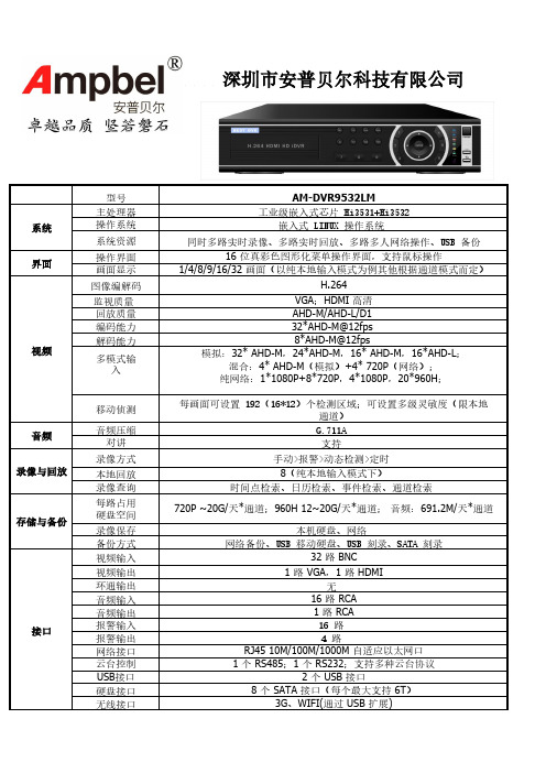
深圳市安普贝尔科技有限公司型号AM-DVR9532LM系统主处理器工业级嵌入式芯片 Hi3531+Hi3532操作系统嵌入式 LINUX 操作系统系统资源同时多路实时录像、多路实时回放、多路多人网络操作、USB 备份界面操作界面16 位真彩色图形化菜单操作界面,支持鼠标操作画面显示1/4/8/9/16/32 画面(以纯本地输入模式为例其他根据通道模式而定)视频图像编解码H.264监视质量 VGA;HDMI 高清回放质量AHD-M/AHD-L/D1编码能力32*AHD-M@12fps解码能力8*AHD-M@12fps多模式输入模拟:32* AHD-M,24*AHD-M,16* AHD-M,16*AHD-L;混合:4* AHD-M(模拟)+4* 720P(网络);纯网络:1*1080P+8*720P,4*1080P,20*960H;移动侦测每画面可设置 192(16*12)个检测区域;可设置多级灵敏度(限本地通道)音频音频压缩G.711A 对讲支持录像与回放录像方式手动>报警>动态检测>定时本地回放8(纯本地输入模式下)录像查询时间点检索、日历检索、事件检索、通道检索存储与备份每路占用硬盘空间720P ~20G/天*通道;960H 12~20G/天*通道;音频:691.2M/天*通道录像保存本机硬盘、网络备份方式网络备份、USB 移动硬盘、USB 刻录、SATA 刻录接口视频输入32 路 BNC视频输出 1 路 VGA,1 路 HDMI环通输出无音频输入16 路 RCA音频输出 1 路 RCA报警输入16 路报警输出 4 路网络接口RJ45 10M/100M/1000M 自适应以太网口云台控制 1 个 RS485;1 个 RS232;支持多种云台协议USB接口 2 个 USB 接口硬盘接口8 个 SATA 接口(每个最大支持 6T)无线接口3G、WIFI(通过 USB 扩展)功能特点:*DVR/HVR/NVR 功能 3 合 1 HD iDVR Three in one:多模式输入,支持 32 路模拟视频编码,支持模拟+网络高清视频混合输入,支持纯高清网络视频输入。
Hi3512 Demo单板用户指南
1 概述1.1 Hi3512 Demo 单板简介Hi3512 Demo 单板是针对海思Hi3512V100 媒体处理芯片开发的参考设计单板,在给客户展示芯片的强大多媒体处理功能和完善接口的同时,更为客户提供Hi3512V100 芯片的硬件参考设计,使客户不需修改或者只需要简单修改参考设计的模块电路,就可以完成同步产品开发;参考设计单板同时支持Hi3512 芯片的SDK 开发、应用软件的开发和运行、芯片验证等目的。
Hi3512 Demo 单板通过串口和网口线与开发PC 连接,作为一个基本开发系统使用,或实现更完全的开发系统或演示环境,此时连接如下设备或部件:电视机或监视器视频源(如模拟摄像头)音频源及音箱USB OTG 从/主设备SATA 硬盘、SD Card 等存储设备红外遥控器USB Wifi无线网卡、3G上网卡鼠标报警输入输出设备Hi3512 Demo 单板最多支持外接4 路CVBS 信号和音频信号,经过Hi3512 Demo单板编码后,将码流传到网络上或存储在本地SATA 硬盘;也可以自行解码后显示。
1.2 Hi3512 Demo 单板功能特性Hi3512 Demo 单板具有以下功能特性:支持4 路CVBS 输入,H264 Main Profile @ Level 3 视频编解码,最大编码能力为D1@60fps 或CIF@240fps支持1 路CVBS 输出支持1 路RJ45 网络接口、支持10M/100M bit/s 和全双工或半双工模式支持1 路立体声或MIC 输入、1 路立体声输出支持1 路USB 2.0 OTG支持1 路USB 1.1 设备支持2 路RS232 标准串口,1200~115200bit/s 波特率;1 路RS485 接口支持IR 红外接收接口支持4路报警输入和2路报警输出(带继电器)支持SD/MMC卡支持实时时钟存储器参数如表1-1 所示。
表1-1 存储器参数表存储器 数据位宽 频率 容量 DDR2 SDRAM 32/16 bit 144M 256MB Nor Flash 8bit - 16MB 以上功能的实现状态以版本发布时的信息为准。
基于Hi3531的视频存储与回放电路的设计
基于Hi3531的视频存储与回放电路的设计作者:金永明来源:《山东工业技术》2016年第14期摘要:本文描述了基于Hi3531处理器为核心的视频存储与回放电路的设计,介绍了电路中重要功能模块设计,同时对与电路相关的驱动软件进行了规划。
本电路实现方便,具有一定的使用价值。
关键词:Hi3531;视频;存储DOI:10.16640/ki.37-1222/t.2016.14.1350 引言随着计算机应用领域地不断扩展,现在人类在工作、学习、生活过程中越来越依靠计算机应用提供的便利,提高工作效率、改善生活质量、激发学习乐趣。
因此,对计算机上应用及操作的监控也是一个重要的研究方向,通过对计算机上应用及操作的实时监控,可以完成计算机应用及操作的事后评估、检索和取证,为检查计算机操作人员的工作准确性和合理性提供视频数据。
对计算机应用和操作进行视频扑获、存储和回放,需要对计算机应用和操作的视频监控。
我们基于Hi3531芯片设计和实现了计算机视频存储和回放电路,可将计算机VGA视频信号扑获,存储在固态电子盘中,利用USB通讯口对存储视频进行回放,电路设计稳定高效,软件使用简易,在视频监控、视频分析、视频检索等应用中具有一定的使用价值。
1 电路原理设计视频存储与回放电路中核心芯片为Hi3531,此芯片是华为公司针对多路高清 DVR、NVR 产品应用开发的一款专业高端SOC 芯片。
芯片中内置高性能双核A9处理器、可完成高达 5 路1080P 视频信号的实时多协议编译码以及专用TOE 网络加速,能应对越来越复杂的高清视频和高速网络应用。
芯片内部集成了优异的视频引擎和编译码算法,结合芯片的多路高清显示输出能力,可以充分满足高质量图像体验。
同时芯片有丰富的外围接口,满足不同项目设计接口的差异化,图1为视频存储与回放电路原理功能框图。
图1中输入视频通过视频环出处理模块后,完成视频信号1:2复制、增强和A/D转换后,提供外部显示终端视频信号,同步提供后继FPGA分辨率转换模块和视频处理模块的视频源,在驱动软件和应用软件控制下,将数字视频信号存储在SSD盘中,供外部主机客户端检索、回放。
Hi3520 硬件设计用户指南

本文档提及的其他所有商标或注册商标,由各自的所有人拥有。
注意
您购买的产品、服务或特性等应受海思公司商业合同和条款的约束,本文档中描述的全部或部分产品、服 务或特性可能不在您的购买或使用范围之内。除非合同另有约定,海思公司对本文档内容不做任何明示或 默示的声明或保证。
由于产品版本升级或其他原因,本文档内容会不定期进行更新。除非另有约定,本文档仅作为使用指导, 本文档中的所有陈述、信息和建议不构成任何明示或暗示的担保。
1.3 典型接口电路设计 ..................................................................................................................................1-10 1.3.1 DDR2 接口 .....................................................................................................................................1-10 1.3.2 USB2.0 Host接口............................................................................................................................1-17 1.3.3 GMAC接口设计.............................................................................................................................1-17 1.3.4 DAC接口设计 ................................................................................................................................1-18 1.3.5 EBI接口信号 ..................................................................................................................................1-19 1.3.6 VO信号 ...........................................................................................................................................1-19 1.3.7 未用的数字管脚的处理 ................................................................................................................1-19
Hi3535 硬件设计 Checklist
文档版本 00B04 (2014-04-02)
海思专有和保密信息 版权所有 © 深圳市海思半导体有限公司
i
Hi3535 硬件设计 Checklist
修订日期 2013-11-12
2013-09-30
2013-08-31
版本 00B03 00B02 00B01
修订说明
第 1 章 Checklist 1.1 芯片电源地的设计要求修改描述。 第 1 章 Checklist 1.1 芯片电源地的设计要求修改上电顺序。 初始版本。
修订记录累积了每次文档更新的说明。最新版本的文档包含以前所有文档版本的更新 内容。
修订日期 2014-04-02
版本 00B04
修订说明
第 1 章 Checklist 1.7 VO 接口与视频接口电路设计要求中新增 BT.1120 信号 高 8bit 和低 8bit 关于 Y\C 信号的描述。 1.15 EFuse 模块设计要求中修改下拉电阻的阻值。
深圳市海思半导体有限公司
地址: 网址: 客户服务电话: 客户服务传真: 客户服务邮箱:
深圳市龙岗区坂田华为基地华为电气生产中心 +86-755-28788858 +86-755-28357515 support@
邮编:518129
1.5 SPI/Nand flash
1.1 芯片电源地的设计要求 ................................................................................................................................. 1 1.2 主芯片时钟电路设计要求 ............................................................................................................................. 1 1.3 复位电路设计要求......................................................................................................................................... 2 1.4 小系统设计要求............................................................................................................................................. 2 1.5 SPI/Nand flash ................................................................................................................................................. 2 1.6 I2C 电路设计要求............................................................................................................................................ 2 1.7 VO 接口与视频接口电路设计要求 ............................................................................................................... 3 1.8 I2S 音频电路设计要求 .................................................................................................................................... 3 1.9 USB2.0 电路设计要求 .................................................................................................................................... 3 1.10 USB3.0 电路设计要求 .................................................................................................................................. 4 1.11 SATA 接口电路要求 ..................................................................................................................................... 4 1.12 ETH 电路设计要求 ....................................................................................................................................... 4 1.13 JTAG 和系统控制电路设计要求.................................................................................................................. 5 1.14 UART 电路设计要求 .................................................................................................................................... 5 1.15 EFuse 模块设计要求..................................................................................................................................... 5 1.16 HDMI 设计 .................................................................................................................................................... 6 1.17 散热设计....................................................................................................................................................... 6
Hi3531 DMO单板用户指南
2 硬件介绍..........................................................................................................................................4
2.1 结构与接口..................................................................................................................................................... 4 2.2 工作原理......................................................................................................................................................... 5 2.3 Hi3531DMO 板上各接口的使用情况............................................................................................................ 6 2.4 I2C 地址 ........................................................................................................................................................... 8
森海塞尔 EM3532 接收机说明书
EM 3532-U Instructions for use38Chapter Contents.............................................................................................................................Page1Brief description, special features (40)2Connections and operating elements (41)3Noise reduction with HiDyn plus™ (42)4Diversity reception (43)5Assembly and mounting, assembly instructions (44)6Connection and mounting of remote antennæ (46)7Selecting the mains voltage / Mains connection (47)8Putting the EM 3532 into operation (48)9Basic functions of the Sennheiser operating menu (49)10Menus / Overview (50)11LC display panel (51)12Setting a receiving frequency, allocating a frequency memory andassigning a channel number (52)13Deleting a receiving frequency, emptying a frequency memory (54)14Setting the receiving frequency via the channel number (55)15Squelch (Muting) (56)16Advanced muting function (57)17Automatic transmitter search tuning – Scan function (58)18Adding a supply voltage for antenna boosters (60)19Stand-by operation (61)20Remote control (62)21Power of the received RF signal (63)22Monitoring the sound signal, headphone connection (64)23Replacing a fuse (65)24Sennheiser transmitters report their battery status (66)25Suitable Sennheiser transmitters (67)26Error checklist (68)27Safety instructions (68)28Recommended accessories (69)29T echnical Data (70)39Thank you for choosing Sennheiser!W e have designed this product to give you reliable operation over many years.Please take a few moments to read these instructions carefully, as we want you to enjoy your new Sennheiser product quickly and to the full.1Brief descriptionWith the EM 3532-U twin receiver, Sennheiser offers the professional user a high-quality state-of-the-art RF receiver with a high level of operational reliability and ease of use. The EM 3532-U receiver together with the suitable hand-held and pocket transmitters permits wireless transmission with studio-quality sound. Due to further optimised PLL and microprocessor technology and the Sennheiser patented HiDyn plus™ noise reduction system, these transmission systems surpass the signal-to-noise ratio and dynamic range of modern CD productions. The true diversity technology of the EM 3532-U receiver ensures interference-free transmission and minimises dropouts in the RF link.Especially for small television studios and theatres, the simultaneous use of several Sennheiser 3000 series receivers – such as the EM 3532-U – is an economical alternative to technically more sophisticated and therefore more expensive multi-channel systems of the 5000 series.Special featuresțPLL microprocessor control, programmablețSennheiser HiDyn plus™ noise reduction systemțHigh transmission reliability due to true diversity receptionțEase of use due to menu-assisted operationțIndication of transmitter battery status and “LOW BATT” warning(only with Sennheiser transmitters transmitting battery status information)țRugged 19” 1 U metal housingțDisconnectable supply voltage for external antenna boostersțRemote-controllable via PC with S-MCD softwarețExternal DC supply 11–18 V oltțAdvanced scan function / transmitter search tuning40412Connections and operating elements ᕡHeadphone socket 1/4 ” (6.3 mm) øᕢHeadphone volume control ᕣMulti-function LC display panel ᕤButtons for selecting and programming the menus ᕥSET/storage button ᕦON / OFF switch ᕧFuse holder and mains voltage selection ᕨ2-pin IEC mains connector ᕩCable grip for mains cable µData interface for connecting a remote computer ¸AF output XLR-3M, balanced ¹Control for the AF output level at the XLR socket ¸ƸAntenna input B ƹDC socket (e.g. for use in an OB van)ƺAntenna input A3Noise reduction with HiDyn plus™Progress you can hear:This receiver is equipped with HiDyn plus™, the Sennheiser noise reduction system that reduces RF interference. It increases the signal-to-noise ratio in wireless audio transmission to up to 110 dB. The 96 dB dynamic range of a CD is thus considerably surpassed.HiDyn plus™ is a wideband compander system which compresses the AF level on the transmitter side in a ratio of 2:1 (related to dB), and expands it in exactly the same way on the receiver side. The optimisation of the dynamic range and the supporting effect of the control amplifier in the transmitter effectively reduce modulation problems.HiDyn plus™ has been specially developed for use in high quality radiomicrophone systems.NoteOnly transmitters which are also equipped with HiDyn plus™ can work correctly incombination with the EM 3532-U receiver. If this is not the case, the dynamicrange is drastically reduced and the transmission sounds blunt and flat. HiDyn plus™cannot be switched off on the EM 3532 receiver.424Diversity receptionThe EM 3532 receiver operates on the “true diversity” principle:A receiving antenna receives not only the electromagnetic waves which reach it by a direct path, but also the reflections of these waves which are created in the room by walls, windows, ceilings and fittings. When these waves are superimposed, destructive interference occurs, which can also be called “field strength gaps”. Repositioning the receiving antenna can bring a solution, provided the transmitter remains in its original position. With mobile transmitters, however (which all radiomicrophones are ), the “field strength gap“ will then occur with a different transmitter position. These “field strength gaps“ can only be eliminated with true diversity receivers.In true diversity, instead of one antenna and one receiver there are now two antennæ and two receiver sections. The antennæ are spatially separated. By means of a comparison circuit, the receiver section with the strongest RF signal is always switched to the common AF output. The risk of the occurrence of “field strength gaps” in both antennæ at the same time is virtually nonexistant.The display panel of the receiver always shows whether the diversity channel switched is channel A or channel B.43445Assembly and mountingUse as a stand-alone receiverWhen using the EM 3532 as a stand-alone receiver, it is easiest to use the supplied telescopic antennæ. They can be mounted quickly and easily to the rear of the receiver and are suitable for all applications where – good reception conditions provided – a wireless transmission system is to be used without a large amount of installation work. The best reception quality, however, is obtained by using remote antennæ (see chapter 6).T o ensure that the receiver is securely mountedon a surface on which it cannot slip, four self-adhesive soft rubber feet are supplied. These feetare stuck into the recesses on the lower side ofthe receiver.Ensure that the recesses are clean and free fromgrease before mounting the feet.NoteDo not use these feet if rack-mountingthe receiver.Mounting the receiver into a rackWith the two supplied rack mount “ears”, the receiver can be mounted into a 19” rack (1 U). The rack mount “ears” are screwed to the receiver on the left and right ቢ.NoteIf you wish to connect the antennæ to the front side, you must pull the cables of theGA 3030-AM antenna mount through the holes on the rack mount “ears” beforemouting the “ears” ቤ.The GA 3030-AM antenna mount (accessory, see chapter 28) allows the antennæ to be connected to the front of the receiver, for example if the rear of the rack is closed.Mount the antenna holders to the right and left to the handles of the receiver ባ. The connection cables, which are firmly fixed to the antenna holders, are connected to the antenna sockets on the rear of the receiver.Assembly instructionsțDo not place the receiver in direct proximity to digitally controlled devices!țSite the receiver as high as possible so that the receiving antennæ have a“free line of sight” to the transmitter antennæ!45466Connection and mounting of remote antennæIf the receiver position is not the best antenna position for optimum reception, you can use remote antennæ and antenna boosters. These are available as accessories.The best reception quality is obtained with the Sennheiser A12 AD-UHF active antenna. Antenna and receiver can be connected with RG 58 co-axial cable. Ready made up antenna cables from Sennheiser are available as accessories with lengths of 1 m, 5 m and 10 m (see chapter 28).ǠT o supply the antenna booster integrated in the A12 AD-UHF active antenna, a supply voltage needs to be added via the antenna sockets (see chapter 18).ǠExternal AB 1036-TV antenna boosters can be used for compensating for cablelosses if the remote antennæ are at a long distance from the receiver. The antenna boosters are connected in the antenna cable line and can be supplied with the DC supply voltage by the EM 3532 via the antenna cables.Essential notes on mounting the antennæțPosition antennæ in the same room in which the transmission takes place!țMaintain a minimum distance of 1 metre from metal objects (including reinforced concrete walls)!țMaintain a minimum distance of 1 metre between receiving antennæ!7Selecting the mains voltageBefore you plug the mains connector into the mains, please check first of allthat the receiver is set to the correct mains voltage!Y ou can change the mains voltage by removing the fuse holder ᕧ with the inserted fuse ቢ, turning it through 180°ባ and inserting it again ቤ. The set voltage can be seen at the top of the fuse holder.Mains connectionInsert the supplied mains cable into socket ᕨ on the receiver and pass the cable through the cable grip ᕩ.Because of the cable grip, the cable cannot slip out of socket ᕨ and interrupt operation.NoteA cable grip is particularly important when the receiver is permanently rackmounted. Inside the rack there are often a large number of cables - a cable gripprevents the cables from pulling each other out.8Putting the EM 3532 into operationThe receivers are switched on separately with the ON / OFF switches ². The respective display panel » is now lit up to show that the receiver is switched on, and the standard display is shown (see chapter 11). The display “MUTE” ቢ (see chapter 15) lights up, and the RF field strength is indicated. If a suitable transmitter is already operating on this frequency, the display “MUTE” is initially lit up for about two seconds. Then the deviation is indicated ባ (modulation, see chapter 21), and the diversity branch in use is now displayed for the first time (see chapter 4).After approx. ten more seconds, the battery status display indicates the (remaining) capacity of the transmitter’s battery or rechargeable accupack, provided the transmitter in use transmits a battery status signal (see chapter 24).NoteThe ON / OFF switch ² works in the secondary circuit of the integrated mainstransformer, and thus only switches the low voltage side. By using a modern magneticcore transformer, the power consumption of a receiver of approx. 1/2 Watt whenswitched off is extremely low. For larger installations with several receivers, acomplete mains disconnection can best be achieved by an additional commonON / OFF switch.The AF connection is via sockets ¸ on the rear. The controls ¹ control the AF signal output level.9Basic functions of the Sennheiser operating menuA special feature of the Sennheiser 3000 series is the similar operation of transmitters and receivers. In stressfull situations, for example on stage or during a live show or presentation, it is important that the receiver is easy to operate and that adjustments to the receiver settings can be made quickly and “without looking”. Therefore, the necessary operating steps for each device must be similar.ᕡPress thẽ/̅buttons to select a menu:By briefly pressing the ̃/̅ buttons, you can jump either forwards or backwards to the next menu. Y our selection is indicated by the corresponding LC dot on the right of the display panel ᕣ.ᕢPress the SET button to get into the setting mode:If you now press the SET button, the corresponding display on the display panel begins to flash, indicating that you are in the setting mode of the selected menu.ᕣPress thẽ/̅buttons to adjust the settings of the selected menu.ᕤPress the SET button to store the setting:T o store a setting, press the SET button until “Sto” briefly appears on the display, indicating that your setting has been stored. The display then switches back to the standard display.Important: Only now is your setting stored!ǠIf you do not press the ̃/̅ buttons or the SET button for more than 30 seconds, the setting mode is automatically left and the display switches back to the standard display.Y ou can discontinue your preselection by briefly (!) pressing the SET button. The display briefly indicates “ESC” and then switches back to the standard display.10Menus / OverviewFREQUENCYindicates the current receiving frequency.(u chapter 12)CHANNELindicates the currently assigned channel number.(u chapter 14)SQUELCHindicates the squelch threshold.(u chapter 15)SCANscans for available RF signals, the receiving frequencyfound is shown on the display.(u chapter 17)BOOSTER FEEDindicates whether the supply voltage for activeantennæ or antenna boosters is switched on oroff. (u chapter 18)STANDBYindicates whether the receiver is set to stand-byoperation. All menus – except for “REMOTE” and“STANDBY” – are then locked. (u chapter 19).REMOTEindicates whether the receiver is set for “computerremote control only”. (u chapter 20).11LC display panelᕡDisplay for the “FREQUENCY” menu. This display can be the receiver’s standard display which always appears after switch-on.ᕢDisplay for the “BOOSTER FEED” menu.ᕣDisplay for the “CHANNEL” menu. This display can also be the receiver’s standard display which always appears after switch-on.ᕤDisplay for the “STANDBY” menu.ᕥAlphanumeric main display, indicates the settings that can be adjusted in the menus.ᕦT en-step bargraph for the received RF signal, with overmodulation display (Peak).ᕧT en-step bargraph for the received AF signal,with overmodulation display (Peak) and “peak hold”.ᕨSix-step bargraph for the transmitter battery status (in %) and“LOW BATT” display if transmitter battery is going flat.ᕩAntenna A is currently receiving (diversity selection).µDisplay for the “REMOTE” menu.¸Reception is muted, “MUTE”.¹Antenna B is currently receiving (diversity selection).ƸMenu selection with display via LC dots.12Setting a receiving frequency, allocating a frequency memory and assigning a channel numberThe EM 3532 receiver has a switchable frequency memory to store a maximum of 32 receiving frequencies with their respective channel numbers. The storing procedure is similar for each entry or modification:ǠPress the ̃/̅ buttons to select the “FREQUENCY” menu. Then press the SET button. The “FREQUENCY MHZ” display on the display panel ᕣ begins to flash:ǠWith the ̃/̅ buttons you can now select a different frequency.The display jumps to the next frequency in 5-kHz steps:ǠWhen you get to the desired frequency, press the SET button until “Sto” briefly appears on the display.ǠY ou now have to check whether the frequency memory(nos. 1 to 32) is allocated correctly.The display indicates the receiving channel with the allocated frequency memory, and the “CHANNEL” display lights up. The display for the frequency memory begins to flash.ǠWith the ̃/̅ buttons you can now select a frequency memory (nos. 1 to 32). If the frequency memory has been assigned a channel number, this is also indicated. If no channel number has been assigned, three “hyphens” appear on the display, indicating that the frequency memory is empty (see chapter 13).ǠHave you set the frequency memory correctly? Press the SET button until “Sto” briefly appears on the display.ǠY ou now have to assign the frequency memory a channel number (from 001 to 255). With larger systems, it is recommended to use the same channel numbers for both transmitters and receivers in order to provide for simpler monitoring of the system. With the ̃/̅buttons you can now select the desired channel number:ǠHave you set the channel number correctly? Press the SET button until “Sto” briefly appears on the display. The display then switches back to the standard display.Only now does the receiver change to the new frequency / channel.For some countries, this menu is locked via a special configuration program, since not all tunable receiving frequencies are approved in these countries. If the “FREQUENCY” menu is selected, “Loc”appears on the display.13Deleting a receiving frequency, emptying a frequency memoryǠY ou can empty a frequency memory if you enter three “hyphens” when assigning a channel number.ǠThe last frequency stored cannot be deleted. If you try to delete the last frequency stored, the display briefly indicates “LASt” and then switches back to the standard display.Y ou can discontinue the programming of this menu by briefly (!) pressing the SET button. The display briefly indicates “ESC” and then switches back to the standard display. The previous settings are kept.If you do not press any of the three programming buttons for more than 30 seconds, the setting mode is automatically left. The display briefly indicates “ESC” and then switches back to the standard display. The previous settings are kept.For some countries, this menu is locked via a special configuration program, since not all tunable receiving frequencies are approved in these countries. If the “FREQUENCY” menu is selected, “Loc”appears on the display.14Setting the receiving frequency via the channel numberIn the “CHANNEL” menu, you can directly change from one stored receiving frequency to the next.ǠPress the ̃/̅ buttons to select the “CHANNEL” menu. Then press the SET button. The “CHANNEL” display on the display panel ᕣ begins to flash:The display indicates the receiving frequency in alternation with the channel number.ǠWith the ̃/̅ buttons you can now select a different channel. The display jumps either forwards or backwards to the next channel. The next channel is not necessarily identical with the next channel number assigned!The display indicates the new channel in alternation with the receiving frequency assigned.NoteIf you have reached the first or the last frequency memory, the display briefly indicates “EndtAb”. Continue with your selection in the opposite direction.ǠHave you selected the desired channel? Press the SET button until “Sto” briefly appears on the display. The display then switches back to the standard display.Only now does the receiver change to the new frequency / channel.15Squelch (Muting)The EM 3532 receiver is equipped with an adjustable squelch which eliminates annoying noise when the transmitters are switched on and off. It also suppresses sudden noise when a transmitter leaves the reception area and there is no longer sufficient transmitter power received by the receiver. The adjustment of the squelch is via the “SQUELCH” menu. The adjustment range is between 0 and 134 (on the display), which corresponds to 0 to up to 100 μV. When the squelch is active, the display “MUTE” is lit up on the display panel. If set to position “0”, the squelch is switched off.ǠPress the ̃/̅ buttons to select the “SQUELCH” menu. Then press the SET button. The LC dot on the left of the text SQUELCH begins to flash and the current value of the squelch is shown on the alphanumeric main display and in the deviation bargraph. For the exact value in μV please refer to the RF level bargraph on the left of the deviation bargraph:ǠWith the ̃/̅ buttons you can now select a squelch threshold between 0 and 134.ǠOnly after having been stored does the new squelch treshold become effective. T o store a setting, press the SET button until “Sto” briefly appears on the display, indicating that your setting has been stored. The display then switches back to the standard display.Y ou can discontinue the programming of this menu by briefly (!) pressing the SET button. The display briefly indicates “ESC” and then switches back to the standard display. The previous settings are kept.If you do not press any of the three programming buttons for more than 30 seconds, the setting mode is automatically left. The display briefly indicates “ESC” and then switches back to the standard display. The previous settings are kept.16Advanced muting functionThis receiver also features AMF (A dvanced M uting F unction). This special electronic feature comes into effect when an RF signal drops by about 40 dB in a short time. The reception is then muted for at least three seconds. AMF thus suppresses the annoying switch-off click when a transmitter is switched off. Because of the delay in switching on again, the PLL circuit of the transmitter has enough time to adjust itself back to the corresponding transmission frequency.ExampleOne possible area of use for AMF is the inaudible change of a hand-held transmitter.If the battery of the first transmitter has run down (display “LOW BATT” on thereceiver), a second transmitter is prepared on the same frequency: insert battery,select transmission channel. Then the first transmitter is switched off, AMF switchesto mute and the second transmitter is switched on. The PLL of transmitter 2 stabilisesitself, AMF switches on again. The whole procedure takes place inaudibly in thebackground while AMF is switched to mute. Without AMF, the switching off,switching on and stabilising of the transmission frequency would have been audiblein the form of possible crackles and whistling noises.AMF can be switched off. As it is coupled with the setting of the normal squelch, its function is cancelled if the squelch is set to position “0” (see chapter 15).17Automatic transmitter search tuning – Scan functionThe EM 3532 receiver features a scan function to scan the frequency range of the tuner for a transmitter.For some countries, this menu is locked via a special configuration program, since not all tunable receiving frequencies are approved in these countries. If the “SCAN” menu is selected, “Loc” appears on the display.ǠPress the ̃/̅ buttons to select the “SCAN” menu. “SCAn” appears on the display:Then press the SET button. The current receiving frequency set appears on the display, and the “FREQUENCY MHZ” display as well as the LC dot on the left of the text SCAN begin to flash.ǠWith the ̃/̅ buttons you can now start the transmitter search tuning either upwards or downwards. During transmitter search tuning, the display indicates:or:ǠIf no transmitter is found, the search tuning stops at the upper or lower limit of the24 MHz frequency window. The display then indicates:ǠIf a transmitter with a strong enough RF signal (higher than the squelch level, but at least5 μV) is found, this frequency is indicated on the display. In addition, the deviation and theRF level of the received signal are indicated via the bargraphs. Y ou can now monitor the sound signal with headphones.Information on how to store the new receiving frequency is given in chapter 12.NoteIf you wish to acquire data from your transmitters in use via this menu, themodulation of the transmitters must not be too high, otherwise frequency deviationsmay occur. The solution to this problem is simple: do not talk into the transmitterwhen the search tuning is activated. In general, it is best to put the transmitterdown!Y ou can discontinue the programming of this menu by briefly (!) pressing the SET button. The display briefly indicates “ESC” and then switches back to the standard display. The previous settings are kept.NoteIn this menu, the display does not switch back to the standard display after 30seconds. The search tuning between the two limits of the frequency window takesabout 12 – 15 seconds, and you should have time enough to write the new frequencydown or to compare it with a frequency table.ǠPress the SET button to leave this menu!18Adding a supply voltage for antenna boostersAntenna boosters can be connected to the antenna inputs of the EM 3532 receiver and can be supplied by the receiver via the antenna cables. The supply voltage can be switched on or off.Both receivers in the EM 3532 should be set to the same setting, i.e. both receiver should be set to either “On” or “OFF”!ǠPress the ̃/̅ buttons to select the “BOOSTER FEED” menu. The current setting – i.e. “On”or “OFF” – is indicated on the display.Then press the SET button. The “BOOSTER FEED” display on the display panel begins to flash.Y ou can now select your desired setting:ǠPress the ̅ button to switch on the booster supply voltage, “On” appears on the display:ǠPress the ̃ button to switch off the booster supply voltage, “OFF” appears on the display:ǠY our setting has to be stored before it becomes effective. T o store a setting, press the SET button until “Sto” briefly appears on the display, indicating that your setting has been stored. The display then switches back to the standard display.If the booster supply voltage is switched on, the “BOOSTER FEED” display on the display panel is lit up.Y ou can discontinue the programming of this menu at any time by briefly (!) pressing the SET button. The previous setting is then kept. If you do not press any of the three programming buttons for more than 30 seconds, the setting mode is automatically left and19Stand-by operationThe EM 3532 receiver can be set to stand-by operation. During stand-by operation, information from the RF section is no longer processed and the AF section is muted (MUTE). All other menus – except for “REMOTE” and “STANDBY” – are locked. If you try to select any other menu, “Loc”appears on the display.ǠPress the ̃/̅ buttons to select the “STANDBY” menu. The current setting – i.e. “On” or “OFF” – is indicated on the display.Then press the SET button. The “STANDBY” display on the display panel begins to flash.Y ou can now select your desired setting:ǠPress the ̅ button to switch on the stand-by operation, “On” appears on the display:ǠPress the ̃ button to switch off the stand-by operation, “OFF” appears on the display:ǠY our setting has to be stored before it becomes effective. T o store a setting, press the SET button until “Sto” briefly appears on the display, indicating that your setting has been stored. The display then switches back to the standard display.If the receiver is set to stand-by operation, the “STANDBY” display on the display panel is lit up.Y ou can discontinue the programming of this menu at any time by briefly (!) pressing the SET button. The previous setting is then kept. If you do not press any of the three programming buttons for more than 30 seconds, the setting mode is automatically left and20Remote controlThe EM 3532 receiver can be set for “computer remote control only”. When set for remote control, all other menus – except for “REMOTE” – are locked. If you try to select any other menu, “Loc”appears on the display.ǠPress the ̃/̅ buttons to select the “REMOTE” menu. The current setting – i.e. “On” or “OFF” – is indicated on the display.Then press the SET button. The “REMOTE” display on the display panel begins to flash.Y ou can now select your desired setting:ǠPress the ̅ button to switch on the remote control, “On” appears on the display:ǠPress the ̃ button to switch off the remote control, “OFF” appears on the display:ǠY our setting has to be stored before it becomes effective. T o store a setting, press the SET button until “Sto” briefly appears on the display, indicating that your setting has been stored. The display then switches back to the standard display.If the receiver is set to remote control, the “REMOTE” display on the display panel is lit up.Y ou can discontinue the programming of this menu at any time by briefly (!) pressing the SET button. The previous setting is then kept. If you do not press any of the three programming buttons for more than 30 seconds, the setting mode is automatically left and the previous setting is also kept.。
hi3531原理图
DESIGNED SHUAIXIANZHI REVIEWED LISI XXXXX
4
HI3531DMO
VER
PART_NUMBER
A 03030001
5
NA
ECA NO
DATE
D
00001234
SHEET 3 OF 32
HUAWEI TECH CO.,LTD. 6
1
2
3
4
5
6
System Power Tree:
60mA
LDO 2.5V 60mA Hi3531
Omitted
1.8VOmitted
DIODE
AIC31
2
3
NOTE:The current value in the Power Tree is just evaluated through datasheet; the actual value will be refreshed after the current being tested.
23.VI/VO SWITCH 0
24.VI/VO SWITCH 1
25.HDMI OUTPUT1
26.Connector for Daughter board and Serial link
27.AIC31 28.I2S Audio Switch
The type and specification of the components refer to the BOM
B 10.ETH PHY0
11.ETH PHY1
B
12.SATA & UART & RTC
13.PCIe0
14.PCIe1
15.VDAC & HDMI0
Hi3516A Hi3516D 硬件设计用户指南
版本 03 02 01
00B04 00B03 00B02
00B01
修订说明
修改 1.1.3、1.2.1 和 1.4 小节 修改 1.2.5 小节 第一次正式版本发布,修改图 1-14 和图 1-15,添加图 118 和图 1-19,2.1.3 小节有新增内容。添加 Hi3516D 的相 关内容。
修改图 1-2 及图 1-17 1.3.3.2 章节,VI 接口中有修改。 第二次临时版本发布 新增第 3 章 ESD 设计建议,其他章节都涉及修改。 初始版本
产品版本 V100 V100
读者对象
本文档(本指南)主要适用于以下工程师: z 技术支持工程师 z 单板硬件开发工程师
修订记录
修订记录累积了每次文档更新的说明。最新版本的文档包含以前所有文档版本的更新 内容。
修订日期 2016-03-28 2015-11-02
版本 05 04
修订说明 1.2.5、1.3.5、1.3.8 小节涉及修改 修改 2.1.3 小节的相关内容
文档版本 05 (2016-03-28)
海思专有和保密信息 版权所有 © 深圳市海思半导体有限公司
i
Hi3516A/Hi3516D 硬件设计 用户指南
前言
修订日期 2015-06-15 2015-02-10 2014-12-20
2014-10-20 2014-09-25 2014-09-14
2014-07-15
Hi3516A/Hi3516D 硬件设计
用户指南
文档版本 发布日期
05 2016-03-28
版权所有 © 深圳市海思半导体有限公司 2014-2016。保留一切权利。
非经本公司书面许可,任何单位和个人不得擅自摘抄、复制本文档内容的部分或全部,并不得以任何 形式传播。
- 1、下载文档前请自行甄别文档内容的完整性,平台不提供额外的编辑、内容补充、找答案等附加服务。
- 2、"仅部分预览"的文档,不可在线预览部分如存在完整性等问题,可反馈申请退款(可完整预览的文档不适用该条件!)。
- 3、如文档侵犯您的权益,请联系客服反馈,我们会尽快为您处理(人工客服工作时间:9:00-18:30)。
第 1 次临时版本发布。
文档版本 02 (2012-11-30)
海思专有和保密信息 版权所有 © 深圳市海思半导体有限公司
v
Hi3531/Hi3532 硬件设计 用户指南
目录
目录
前 言................................................................................................................................................iii
1.2.7 增加“Hi3531 SPI 控制接口的片选信号 SPI_CSN6(管脚 AA33)”的注意事项。 第 3 章 单板热设计建议 增加 Hi3532 的散热片选择的相关描述。
文档版本 02 (2012-11-30)
海思专有和保密信息 版权所有 © 深圳市海思半导体有限公司
iv
Hi3531/Hi3532 硬件设计 用户指南
深圳市海思半导体有限公司
地址: 网址: 客户服务电话: 客户服务传真: 客户服务邮箱:
深圳市龙岗区坂田华为基地华为电气生产中心 +86-755-28788858 +86-755-28357515 support@
邮编:518129
Hi3531/Hi3532 硬件设计 用户指南
前言
前言
概述
本文档主要介绍 Hi3531/Hi3532 芯片方3531/Hi3532 芯片的硬件设计方法。
产品版本
与本文档相对应的产品版本如下。
产品名称 Hi3531 芯片 Hi3532 芯片
产品版本 V100 V100
读者对象
本文档(本指南)主要适用于以下工程师: z 技术支持工程师 z 单板硬件开发工程师
修订记录
修订记录累积了每次文档更新的说明。最新版本的文档包含以前所有文档版本的更新 内容。
修订日期 2012-11-30
版本 02
修订说明
第 3 章 单板热设计建议 更新 3.1 节
Hi3531/Hi3532 硬件设计
用户指南
文档版本 发布日期
02 2012-11-30
版权所有 © 深圳市海思半导体有限公司 2011-2012。保留一切权利。
非经本公司书面许可,任何单位和个人不得擅自摘抄、复制本文档内容的部分或全部,并不得以任 何形式传播。
商标声明
、
、海思和其他海思商标均为深圳市海思半导体有限公司的商标。
文档版本 02 (2012-11-30)
海思专有和保密信息 版权所有 © 深圳市海思半导体有限公司
iii
Hi3531/Hi3532 硬件设计 用户指南
前言
修订日期 2012-09-21
2012-06-30
版本 01
00B20
修订说明
1.1.5 Power Supply 电路中增加电源的上下电时序图;增 加 PLL 电源和芯片的 DVDD10 和 DVDD33 电源的隔离磁 珠的要求。
增加图 1-9。 修正了 DDR 关于全驱和半驱的说法。 1.2.10 模拟 DAC 接口设计 VDAC1_IREF 外接并联到地的 1%精密电阻中的 680Ω 改 为 1.1KΩ.。 刷新 1.2.4 FLASH 接口设计的部分描述。 刷新 1.2.7 SPI 控制接口设计的部分描述。 2.2.1 电源设计中,删除“电源管脚摆放的去耦电容,并 且在 PCB 上对 VREF 加包地屏蔽处理”的描述。 刷新 2.3 GMAC 布线设计建议的部分描述。 刷新 2.4 USB 接口电路设计建议的部分描述。 刷新 2.5 PCIE 总线 PCB 设计建议的部分描述。 修改 Hi3532 的散热片尺寸。
Hi3531 的内核电压及相关描述由 1.0V 改为 1.03V; Hi3532 的内核电压及相关描述由 1.0V 改为 1.15V 第 1 章 原理图设计建议 1.2.1.1 删除“支持 DDR3L,即在 DDR3 时,支持 1.35V”的描述。 1.2.1.3 外接 DDR3 时,删除采用 Fly-by 拓扑结构的相关 描述及示意图
本文档提及的其他所有商标或注册商标,由各自的所有人拥有。
注意
您购买的产品、服务或特性等应受海思公司商业合同和条款的约束,本文档中描述的全部或部分产 品、服务或特性可能不在您的购买或使用范围之内。除非合同另有约定,海思公司对本文档内容不 做任何明示或默示的声明或保证。
由于产品版本升级或其他原因,本文档内容会不定期进行更新。除非另有约定,本文档仅作为使用 指导,本文档中的所有陈述、信息和建议不构成任何明示或暗示的担保。
1 原理图设计建议.............................................................................................................................. 1
1.1 小系统外部电路要求 ..................................................................................................................................... 1 1.1.1 Clocking 电路......................................................................................................................................... 1 1.1.2 复位和 Watchdog 电路.......................................................................................................................... 1 1.1.3 JTAG Debug 接口 .................................................................................................................................. 2 1.1.4 Hi3531/Hi3532 硬件初始化系统配置电路........................................................................................... 3 1.1.5 Power Supply 电路 ................................................................................................................................. 5
1.2 Hi3531/Hi3532 接口电路设计........................................................................................................................ 7 1.2.1 DDR2/3 接口 .......................................................................................................................................... 7 1.2.2 USB2.0 Host 接口 ................................................................................................................................ 15 1.2.3 GMAC 接口设计.................................................................................................................................. 16 1.2.4 FLASH 接口设计................................................................................................................................. 18 1.2.5 PCIe 接口设计...................................................................................................................................... 18 1.2.6 SATA 接口设计.................................................................................................................................... 19 1.2.7 SPI 控制接口设计............................................................................................................................... 19 1.2.8 I2S 接口设计......................................................................................................................................... 20 1.2.9 HDMI 输出接口设计 ........................................................................................................................... 20 1.2.10 模拟 DAC 接口设计 ......................................................................................................................... 20 1.2.11 VI/VO 接口设计................................................................................................................................. 21