Diode Laser Soldering Technology of Fine Pitch QFP Devices
SMT英文缩写词汇解析和部分SMT术语详解

SMT英文缩写词汇解析AI :Auto-Insertion 自动插件AQL :acceptable quality level 允收水准ATE :automatic test equipment 自动测试ATM :atmosphere 气压BGA :ball grid array 球形矩阵CCD :charge coupled device 监视连接组件(摄影机)CLCC :Ceramic leadless chip carrier 陶瓷引脚载具COB :chip-on-board 芯片直接贴附在电路板上cps :centipoises(黏度单位) 百分之一CSB :chip scale ball grid array 芯片尺寸BGACSP :chip scale package 芯片尺寸构装CTE :coefficient of thermal expansion 热膨胀系数DIP :dual in-line package 双内线包装(泛指手插组件)FPT :fine pitch technology 微间距技术FR-4 :flame-retardant substrate 玻璃纤维胶片(用来制作PCB材质) IC :integrate circuit 集成电路IR :infra-red 红外线Kpa :kilopascals(压力单位)LCC :leadless chip carrier 引脚式芯片承载器MCM :multi-chip module 多层芯片模块MELF :metal electrode face 二极管MQFP :metalized QFP 金属四方扁平封装NEPCON :National Electronic Package andProduction Conference 国际电子包装及生产会议PBGA:plastic ball grid array 塑料球形矩阵PCB:printed circuit board 印刷电路板PFC :polymer flip chipPLCC:plastic leadless chip carrier 塑料式有引脚芯片承载器Polyurethane 聚亚胺酯(刮刀材质)ppm:parts per million 指每百万PAD(点)有多少个不良PAD(点)psi :pounds/inch2 磅/英吋2PWB :printed wiring board 电路板QFP :quad flat package 四边平坦封装SIP :single in-line packageSIR :surface insulation resistance 绝缘阻抗SMC :Surface Mount Component 表面黏着组件SMD :Surface Mount Device 表面黏着组件SMEMA :Surface Mount EquipmentManufacturers Association 表面黏着设备制造协会SMT :surface mount technology 表面黏着技术SOIC :small outline integrated circuitSOJ :small out-line j-leaded packageSOP :small out-line package 小外型封装SOT :small outline transistor 晶体管SPC :statistical process control 统计过程控制SSOP :shrink small outline package 收缩型小外形封装TAB :tape automaticed bonding 带状自动结合TCE :thermal coefficient of expansion 膨胀(因热)系数Tg :glass transition temperature 玻璃转换温度THD :Through hole device 须穿过洞之组件(贯穿孔)TQFP :tape quad flat package 带状四方平坦封装UV :ultraviolet 紫外线uBGA :micro BGA 微小球型矩阵cBGA :ceramic BGA 陶瓷球型矩阵PTH :Plated Thru Hole 导通孔IA Information Appliance 信息家电产品MESH 网目OXIDE 氧化物FLUX 助焊剂LGA (Land Grid Arry)封装技术 LGA封装不需植球,适合轻薄短小产品应用。
半导体激光器相关的英语单词
半导体激光器相关的英语单词Semiconductor lasers are a pretty cool technology. They use materials like silicon and germanium to create focused beams of light. And you know what? They're tiny! You canfit a whole laser in your palm.When it's about efficiency, semiconductor lasers really shine. They convert electricity to light with hardly any waste. That's why they're used in so many applications, from medical devices to communications.Talking about communications, did you know that semiconductor lasers are the backbone of fiber-optic networks? They send signals over long distances with almost no loss. Imagine all that data flowing through tiny beams of light!And when it's about precision, these lasers are unmatched. They can cut materials with extreme accuracy, making them indispensable in manufacturing. Whether it's amicrochip or a piece of jewelry, semiconductor lasersensure perfect cuts.But did you know they're also fun? With the right setup, you can create amazing light displays with semiconductor lasers. They're often used in concerts and events to create stunning visual effects.So there you have it – a quick peek into the world of semiconductor lasers. From efficiency to precision to entertainment, they're truly remarkable pieces of technology.。
半导体激光器 折射率 电流

半导体激光器折射率电流英文回答:Semiconductor lasers, also known as diode lasers, are devices that generate coherent light through the process of stimulated emission. These lasers are widely used in various applications such as telecommunications, optical storage, and laser printing. One of the important factors that affect the performance of semiconductor lasers is the refractive index.The refractive index of a material determines how light propagates through it. In the case of semiconductor lasers, the refractive index of the active region, where the laser light is generated, plays a crucial role in determining the laser's characteristics. By adjusting the refractive index, one can control the wavelength and output power of the laser.The refractive index of a semiconductor material can bemodified by changing the composition of the material or by applying an external electric field. For example, by varying the concentration of dopants in the active region, one can change the refractive index and thus the wavelength of the emitted light. This is the principle behind tunable semiconductor lasers.Another important parameter that affects the performance of semiconductor lasers is the current. The current flowing through the laser diode determines the number of electrons and holes that are available for the process of stimulated emission. By increasing the current, one can increase the population inversion and thus the output power of the laser.However, increasing the current beyond a certain point can also lead to undesirable effects such as thermal runaway and catastrophic optical damage. Thermal runaway occurs when the heat generated by the laser exceeds its ability to dissipate heat, leading to a rapid increase in temperature and a decrease in performance. Catastrophic optical damage occurs when the laser is operated at highcurrents for an extended period, leading to irreversible damage to the laser diode.To optimize the performance of semiconductor lasers, it is important to carefully control the current and monitor the temperature. This can be achieved through the use of feedback control systems that adjust the current and temperature based on the laser's operating conditions. By maintaining the laser within its safe operating range, one can ensure reliable and efficient operation.中文回答:半导体激光器,也被称为二极管激光器,是通过受激辐射的过程产生相干光的装置。
半导体激光基本原理

半导体激光基本原理English:Semiconductor lasers, also known as diode lasers, operate by using the principle of stimulated emission to generate coherent light. They are typically constructed from a semiconductor diode structure, and when a current is applied to the diode, it generates a population inversion of electrons and holes in the active region. This results in the emission of photons as the electrons transition from the higher energy state to the lower energy state. The photons then bounce back and forth between the mirrors at either end of the diode, stimulating further emission and amplifying the light. This process ultimately leads to the production of a highly concentrated, directional, and monochromatic beam of light, which is the defining characteristic of a laser.中文翻译:半导体激光器,也称为二极管激光器,通过使用受激发射原理来产生相干光。
SMT术语英语
Smt属于转换英语THT(Through Hole Technology):通孔安装技术SMT(Surface Mounted Technology):表面安装技术PTH (Pin Through the Hole):通孔安装THT (Through Hole Component) :通孔插装元件SMB (Surface Mount Printed Circuit Board):表面安装PCB板SMC (Surface Mount Component):表面安装元件SMD (Surface Mount Device):表面安装器件SMA (Surface Mount Assembly):表面安装组件Component:元件Device:器件Assembly:组件CTE(coefficient of thermal expansion):热膨胀系数In-circuit test:在线测试Lead configuration:引脚外形Placement equipment:贴装设备Reflow soldering:回流焊接Repair:修理Rework:返工Solderability:可焊性Soldermask:阻焊Yield:产出率Packaging density:装配密度Chip:片状元件melf:圆柱形元件PCB(Printed circuit board):印刷电路板DIP:双列直插SIP:单列直插SOT(Small Outline Transistor):小外形晶体管SOIC(Small outline IC):小外形集成电路,SOP(Small outline Package):小外型封装PLCC(Plastic Leaded Chip Carrier):塑型有引脚芯片载体LCCC(Leadless Ceramic Chip Carrier):无引脚陶瓷芯片载体QFP(Quad Flat Package):多引脚方形扁平封装BGA(Ball grid array)球栅列阵CSP(Chip Scale Package):芯片规模的封装Bare Chip:裸芯片Accuracy:精度ATE(Automated test equipment):自动测试设备AOI(Automatic optical inspection):自动光学检查Blind via:盲孔Buried via:埋孔through via:通孔Bridge:锡桥Circuit tester:电路测试机CTE(Coefficient of the thermal expansion):温度膨胀系数Cold solder joint:冷焊锡点Component density:元件密度Copper foil:铜箔Copper mirror test:铜镜测试Cure:烘焙固化Cycle rate:循环速率Defect:缺陷Desoldering:卸焊Downtime:停机时间FPT(Fine-pitch technology):密脚距技术Flip chip:倒装芯片FCT(Functional test):功能测试Golden boy:金样ICT(In-circuit test):在线测试JIT(Just-in-time):刚好准时Lead configuration:引脚外形Packaging density:装配密度Pick-and-place:拾取-贴装设备Placement equipment:贴装设备Reflow soldering:回流焊接Repair:修理Rework:返工Defect SoldeR少锡Schematic:原理图Solder bump:焊锡球Solderability:可焊性Soldermask:阻焊Tape-and-reel:带和盘Tombstoning:元件立起Ultra-fine-pitch:超密脚距Yield:产出率solder mask:阻焊漆silk screen:丝印面via:导孔Copper Clad Laminates:覆铜箔层压板past mask:焊膏膜(漏板)solder mask:焊接掩摸(阻焊膜)Solding Pasts:焊锡膏Stencils:模板、漏板、钢板Bridging:搭锡Cursting:发生皮层Excessive Paste:膏量太多Insufficient Paste:膏量不足Poor Tack Retention:粘着力不足Slumping:坍塌Smearing:模糊Dpm(defects per million):百万缺陷率Flexibility:柔性Modularity:模块化Component Pick-Up:元件拾取Component Check:元件检查Component Transport:元件传送Placement Procedure:元件放置Chamber System:炉膛系统Blowholes:吹孔Voids:空洞Movement:移位Misalignment:偏斜Dewetting:缩锡Dull Joint:焊点灰暗Non-Dewetting:不沾锡Accuracy:精度Additive Process:加成工艺Adhesion:附着力Aerosol:气溶剂Angle of attack:迎角Anisotropic adhesive:各异向性胶Annular ring:环状圈Application specific integrated circuit :ASIC特殊应用集成电路Array:列阵Artwork:布线图Automated test equipment:ATE自动测试设备Bond lift-off:焊接升离Bonding agent:粘合剂CAD/CAM system:计算机辅助设计与制造系统Capillary action:毛细管作用Chip on board :COB板面芯片Circuit tester:电路测试机Cladding:覆盖层Cold cleaning:冷清洗Cold solder joint:冷焊锡点Conductive epoxy:导电性环氧树脂Conductive ink:导电墨水Conformal coating:共形涂层Copper foil:铜箔Copper mirror test:铜镜测试Cure:烘焙固化nought materiel 无料Cycle rate:循环速率Data recorder:数据记录器Defect:缺陷Delamination:分层Desoldering:卸焊Dewetting:去湿DFM:为制造着想的设计Dispersant:分散剂Documentation:文件编制Downtime:停机时间Durometer:硬度计Environmental test:环境测试Eutectic solders:共晶焊锡Fiducial:基准点Fillet:焊角Fine-pitch technology :FPT密脚距技术Fixture:夹具Full liquidus temperature:完全液化温度Golden boy:金样Halides:卤化物Hard water:硬水Hardener:硬化剂Line certification:生产线确认Machine vision:机器视觉Mean time between failure :MTBF平均故障间隔时间Nonwetting:不熔湿的Organic activated :OA有机活性的Packaging density:装配密度Photoploter:相片绘图仪Placement equipment:贴装设备Repeatability:可重复性Rheology:流变学Schematic:原理图Semi-aqueous cleaning:不完全水清洗Shadowing:阴影Silver chromate test:铬酸银测试Slump:坍落Solder bump:焊锡球Solderability:可焊性Soldermask:阻焊Solids:固体Solidus:固相线Statistical process control :SPC统计过程控制Storage life:储存寿命Subtractive process:负过程Surfactant:表面活性剂Syringe:注射器Tape-and-reel:带和盘Thermocouple:热电偶Tombstoning:元件立起Vapor degreaser:汽相去油器paste working 1ife:焊膏工作寿命paste shelf life:焊膏贮存寿命slump:塌落no-clean solder paste:免清洗焊膏low temperature paste:低温焊膏screen printing:丝网印刷screen printing plate:网版squeegee:刮板screen printer:丝网印刷机stencil printing:漏版印刷metal stencil:金属漏版flexible stencil:柔性金属漏版feeders:供料器tape feeder:带式供料器stick feeder:杆式供料器tray feeder:盘式供料器bulk feeder:散装式供料器feeder holder:供料器架placement accuracy:贴装精度shifting deviation:平移偏差rotating deviation:旋转偏差resolution:分辨率repeatability:重复性placement speed:贴装速度low speed placement equipment:低速贴装机general placement equipment:中速贴装机high speed placement equipment:高速贴装机precise placement equipment:精密贴装机optic correction system :光学校准系统sequential placement:顺序贴装placement pressure:贴装压力placement direction:贴装方位flying:飞片flux bubbles:焊剂气泡dual wave soldering:双波峰焊self alignment:自定位skewing:偏移tomb stone effect:墓碑现象Manhattan effect:曼哈顿现象hot air reflow soldering:热风再流焊convection reflow soldering:热对流再流焊laser reflow soldering:激光再流焊vapor phase soldering(VPS):气相再流焊located soldering:局部软钎焊cleaning after soldering:焊后清洗AI :Auto-Insertion 自動插件AQL :acceptable quality level 允收水準ATE :automatic test equipment 自動測試ATM :atmosphere 氣壓BGA :ball grid array 球形矩陣CCD :charge coupled device 監視連接元件(攝影機)CLCC :Ceramic leadless chip carrier 陶瓷引腳載具COB :chip-on-board 晶片直接貼附在電路板上cps :centipoises(黏度單位) 百分之一CSB :chip scale ball grid array 晶片尺寸BGACSP :chip scale package 晶片尺寸構裝CTE :coefficient of thermal expansion 熱膨脹系數DIP :dual in-line package 雙內線包裝(泛指手插元件)FPT :fine pitch technology 微間距技術FR-4 :flame-retardant substrate 玻璃纖維膠片(用來製作PCB材質) IC :integrate circuit 積體電路IR :infra-red 紅外線Kpa :kilopascals(壓力單位)LCC :leadless chip carrier 引腳式晶片承載器MCM :multi-chip module 多層晶片模組MELF :metal electrode face 二極體MQFP :metalized QFP 金屬四方扁平封裝NEPCON :National Electronic Package andProduction Conference 國際電子包裝及生產會議PBGA:plastic ball grid array 塑膠球形矩陣PCB:printed circuit board 印刷電路板PFC :polymer flip chipPLCC:plastic leadless chip carrier 塑膠式有引腳晶片承載器Polyurethane 聚亞胺酯(刮刀材質)ppm:parts per million 指每百萬PAD(點)有多少個不良PAD(點)psi :pounds/inch2 磅/英吋2PWB :printed wiring board 電路板QFP :quad flat package 四邊平坦封裝SIP :single in-line packageSIR :surface insulation resistance 絕緣阻抗SMC :Surface Mount Component 表面黏著元件SMD :Surface Mount Device 表面黏著元件SMEMA :Surface Mount EquipmentManufacturers Association 表面黏著設備製造協會SMT :surface mount technology 表面黏著技術SOIC :small outline integrated circuitSOJ :small out-line j-leaded packageSOP :small out-line package 小外型封裝SOT :small outline transistor 電晶體SPC :statistical process control 統計過程控制SSOP :shrink small outline package 收縮型小外形封裝TAB :tape automaticed bonding 帶狀自動結合TCE :thermal coefficient of expansion 膨脹(因熱)係數Tg :glass transition temperature 玻璃轉換溫度THD :Through hole device 須穿過洞之元件(貫穿孔)TQFP :tape quad flat package 帶狀四方平坦封裝UV :ultraviolet 紫外線uBGA :micro BGA 微小球型矩陣cBGA :ceramic BGA 陶瓷球型矩陣PTH :Plated Thru Hole 導通孔IA Information Appliance 資訊家電產品MESH 網目OXIDE 氧化物FLUX 助焊劑LGA (Land Grid Arry)封裝技術LGA封裝不需植球,適合輕薄短小產品應用。
SMT专业术语
SMT专业术语我这里有一些关于SMT的专业术语,和大家分享。
AI :Auto-Insertion 自動插件AQL :acceptable quality level 允收水準ATE :autom atic test equipment 自動測試ATM :atm osphere 氣壓BGA :ball grid array 球形矩陣CCD :charge coupled device 監視連接元件(攝影機)CLCC :Ceramic leadless chip carrier 陶瓷引腳載具COB :chip-on-board 晶片直接貼附在電路板上cps :centipoises(黏度單位) 百分之一CSB :chip scale ball grid array 晶片尺寸BGACSP :chip scale package 晶片尺寸構裝CTE :coefficient of therm al expansion 熱膨脹系數DIP :dual in-line package 雙內線包裝(泛指手插元件)FPT :fine pitch technology 微間距技術FR-4 :flame-retardant substrate 玻璃纖維膠片(用來製作PCB材質) IC :integrate circuit 積體電路IR :infra-red 紅外線Kpa :kilopascals(壓力單位)LCC :leadless chip carrier 引腳式晶片承載器MCM :multi-chip m odule 多層晶片模組MELF :m etal electrode face 二極體MQFP :m etalized QFP 金屬四方扁平封裝NEPCON :National Electronic Package andProduction Conference 國際電子包裝及生產會議PBGA lastic ball grid array 塑膠球形矩陣PCB rinted circuit board 印刷電路板PFC olym er flip chipPLCC lastic leadless chip carrier 塑膠式有引腳晶片承載器Polyurethane 聚亞胺酯(刮刀材質)ppm arts per m illion 指每百萬PAD(點)有多少個不良PAD(點)psi ounds/inch2 磅/英吋2PWB rinted wiring board 電路板QFP :quad flat package 四邊平坦封裝SIP :single in-line packageSIR :surface insulation resistance 絕緣阻抗SMC :Surface Mount Com ponent 表面黏著元件SMD :Surface Mount Device 表面黏著元件SMEMA :Surface Mount EquipmentManufacturers Association 表面黏著設備製造協會SMT :surface m ount technology 表面黏著技術SOIC :sm all outline integrated circuitSOJ :sm all out-line j-leaded packageSOP :sm all out-line package 小外型封裝SOT :sm all outline transistor 電晶體SPC :statistical process control 統計過程控制SSOP :shrink sm all outline package 收縮型小外形封裝TAB :tape autom aticed bonding 帶狀自動結合TCE :therm al coefficient of expansion 膨脹(因熱)係數Tg :glass transition temperature 玻璃轉換溫度THD :Through hole device 須穿過洞之元件(貫穿孔)TQFP :tape quad flat package 帶狀四方平坦封裝UV :ultraviolet 紫外線uBGA :micro BGA 微小球型矩陣cBGA :ceramic BGA 陶瓷球型矩陣PTH :Plated Thru Hole 導通孔IA Information Appliance 資訊家電產品MESH 網目OXIDE 氧化物FLUX 助焊劑LGA (Land Grid Arry)封裝技術LGA封裝不需植球,適合輕薄短小產品應用。
铝合金焊接接头的力学性能测试
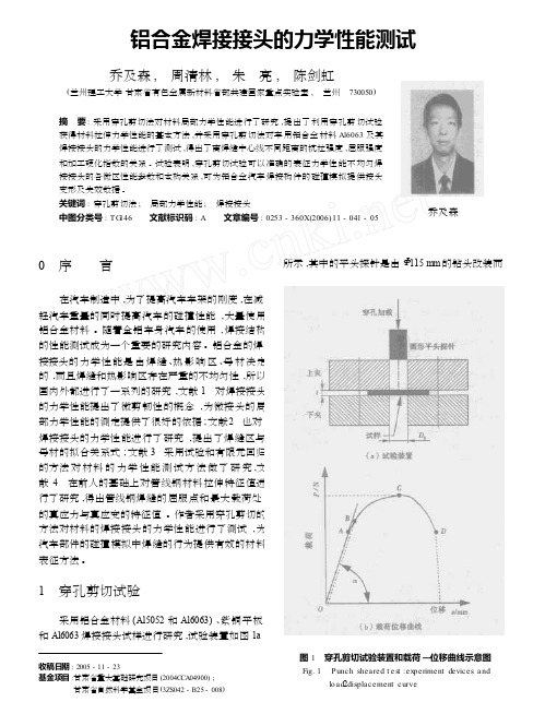
铝合金焊接接头的力学性能测试乔及森 , 周清林 , 朱 亮 , 陈剑虹(兰州理工大学 甘肃省有色金属新材料省部共建国家重点实验室 , 兰州 730050)摘 要 : 采用穿孔剪切法对材料局部力学性能进行了研究 ,提出了利用穿孔剪切试验 获得材料拉伸力学性能的基本方法 ,并采用穿孔剪切法对车用铝合金材料 Al6063 及其 焊接接头的力学性能进行了测试 ,得出了离焊缝中心线不同距离的抗拉强度 ,屈服强度 和加工硬化指数的关系 。
试验表明 ,穿孔剪切试验可以准确的表征力学性能不均匀焊 接接头的各微区性能参数和本构关系 ,可为铝合金汽车焊接构件的碰撞模拟提供接头 变形及失效数据 。
关键词 : 穿孔剪切法 ; 局部力学性能 ; 焊接接头 乔及森中图分类号 : TG 146文献标识码 : A文章编号 : 0253 - 360X (2006) 11 - 041 - 05所示 ,其中的平头探针是由 Φ115 mm 的钻头改装而0 序 言在汽车制造中 ,为了提高汽车车架的刚度 ,在减 轻汽车重量的同时提高汽车的碰撞性能 ,大量使用 铝合金材料 。
随着全铝车身汽车的使用 ,焊接结构 的性能测试成为一个重要的研究内容 。
铝合金的焊 接接头的力学性能是 由 焊 缝 、热 影 响 区 、母 材 决 定 的 ,而且焊缝和热影响区存在严重的不均匀性 ,所以 国内外都进行了一系列的研究 ,文献 1 对焊接接头 的力学性能提出了微剪韧性的概念 ,为微接头的局 部力学性能的测定提供了很好的依据 ;文献 2 也对 焊接接头的力学性能进行了研究 ,提出了焊缝区与 母材的拟合关系式 ;文献 3 采用试验和有限元回归 的方法 对 材 料 的 力 学 性 能 测 试 方 法 做 了 研 究 , 文 献 4 在前人的基础上对管线钢材料拉伸特征值进 行了研究 ,得出管线钢焊缝的屈服点和最大载荷处 的真应力与真应变的特征值 。
作者采用穿孔剪切的 方法对材料的焊接接头的力学性能进行了测试 ,为 汽车部件的碰撞模拟中焊缝的行为提供有效的材料 表征方法 。
SMT行业常用名词缩写中英文对照

SMT行业常用名词缩写中英文对照AI :Auto—Insertion 自動插件AQL :acceptable quality level 允收水準ATE :automatic test equipment 自動測試ATM :atmosphere 氣壓BGA :ball grid array 球形矩陣CCD :charge coupled device 監視連接元件(攝影機)CLCC :Ceramic leadless chip carrier 陶瓷引腳載具COB :chip-on—board 晶片直接貼附在電路板上cps :centipoises(黏度單位) 百分之一CSB :chip scale ball grid array 晶片尺寸BGACSP :chip scale package 晶片尺寸構裝CTE :coefficient of thermal expansion 熱膨脹系數DIP :dual in-line package 雙內線包裝(泛指手插元件)FPT :fine pitch technology 微間距技術FR-4 :flame—retardant substrate 玻璃纖維膠片(用來製作PCB材質) IC :integrate circuit 積體電路IR :infra—red 紅外線Kpa :kilopascals(壓力單位)LCC :leadless chip carrier 引腳式晶片承載器MCM :multi—chip module 多層晶片模組MELF :metal electrode face 二極體MQFP :metalized QFP 金屬四方扁平封裝NEPCON :National Electronic Package andProduction Conference 國際電子包裝及生產會議PBGA:plastic ball grid array 塑膠球形矩陣PCB:printed circuit board 印刷電路板PFC :polymer flip chipPLCC:plastic leadless chip carrier 塑膠式有引腳晶片承載器Polyurethane 聚亞胺酯(刮刀材質)ppm:parts per million 指每百萬PAD(點)有多少個不良PAD(點)psi :pounds/inch2 磅/英吋2PWB :printed wiring board 電路板QFP :quad flat package 四邊平坦封裝SIP :single in—line packageSIR :surface insulation resistance 絕緣阻抗SMC :Surface Mount Component 表面黏著元件SMD :Surface Mount Device 表面黏著元件SMEMA :Surface Mount EquipmentManufacturers Association 表面黏著設備製造協會SMT :surface mount technology 表面黏著技術SOIC :small outline integrated circuitSOJ :small out—line j—leaded packageSOP :small out—line package 小外型封裝SOT :small outline transistor 電晶體SPC :statistical process control 統計過程控制SSOP :shrink small outline package 收縮型小外形封裝TAB :tape automaticed bonding 帶狀自動結合TCE :thermal coefficient of expansion 膨脹(因熱)係數Tg :glass transition temperature 玻璃轉換溫度THD :Through hole device 須穿過洞之元件(貫穿孔)TQFP :tape quad flat package 帶狀四方平坦封裝UV :ultraviolet 紫外線uBGA :micro BGA 微小球型矩陣cBGA :ceramic BGA 陶瓷球型矩陣PTH :Plated Thru Hole 導通孔IA Information Appliance 資訊家電產品MESH 網目OXIDE 氧化物FLUX 助焊劑LGA (Land Grid Arry)封裝技術LGA封裝不需植球,適合輕薄短小產品應用.TCP (Tape Carrier Package)ACF Anisotropic Conductive Film 異方性導電膠膜製程Solder mask 防焊漆Soldering Iron 烙鐵Solder balls 錫球Solder Splash 錫渣Solder Skips 漏焊Through hole 貫穿孔Touch up 補焊Briding 穚接(短路)Solder Wires 焊錫線Solder Bars 錫棒Green Strength 未固化強度(紅膠)Transter Pressure 轉印壓力(印刷)Screen Printing 刮刀式印刷Solder Powder 錫顆粒Wetteng ability 潤濕能力Viscosity 黏度Solderability 焊錫性Applicability 使用性Flip chip 覆晶Depaneling Machine 組裝電路板切割機Solder Recovery System 錫料回收再使用系統Wire Welder 主機板補線機X-Ray Multi-layer Inspection System X—Ray孔偏檢查機BGA Open/Short X—Ray Inspection Machine BGA X—Ray檢測機Prepreg Copper Foil Sheeter P.P。