vlsi circuit design 10 multipliers hit
详解Multisim-10对单片机仿真实验步骤
详解Multisim 10仿真实验步骤时间:2010-06-22 04:19:17 来源:作者:一、实验目的熟悉并掌握Multisim10对单片机的仿真过程。
加深对单片机硬件以及软件理论知识的理解。
二、实验原理1、Multisim10美国国家仪器公司下属的ElectroNIcs Workbench Group在今年年初发布了Multisim 10。
新版的Multisim10,加入了MCU模块功能,可以和8051等单片机进行编程联调,该软件元件丰富,界面直观,虚拟仪器的逼真度达到了让人相当高的程度,是电子设计、电路调试、虚拟实验必备良件。
工程师们可以使用Multisim 10交互式地搭建电路原理图,并对电路行为进行仿真。
Multisim提炼了SPICE仿真的复杂内容,这样工程师无需懂得深入的SPICE技术就可以很快地进行捕获、仿真和分析新的设计,这也使其更适合电子学教育。
通过Multisim和虚拟仪器技术,PCB设计工程师和电子学教育工作者可以完成从理论到原理图捕获与仿真再到原型设计和测试这样一个完整的综合设计流程。
下面将简单介绍一下Multisim10刚加进来的MCU模块的使用方法。
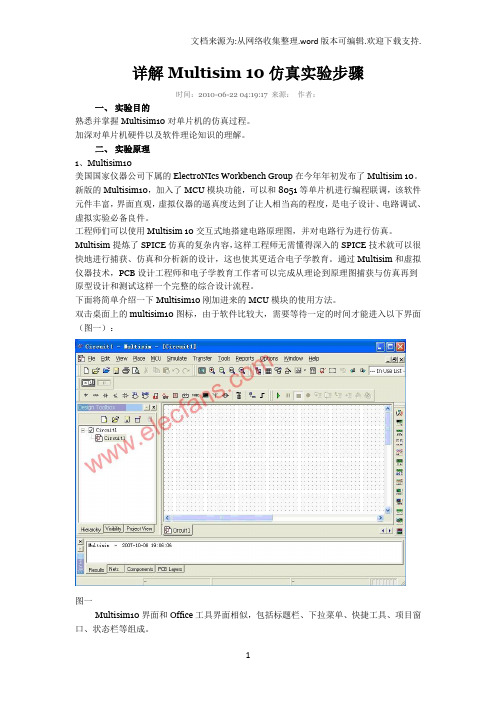
双击桌面上的multisim10图标,由于软件比较大,需要等待一定的时间才能进入以下界面(图一):图一Multisim10界面和Office工具界面相似,包括标题栏、下拉菜单、快捷工具、项目窗口、状态栏等组成。
标题栏用于显示应用程序名和当前的文件名。
下拉菜单提供各种选项。
快捷工具分为:文件工具按钮,器件工具按钮,调试工具按钮,这些按钮在下拉菜单中都有,并经常用到,现在放在工具栏里是为了方便使用。
项目窗口中的电路窗口是用来搭建电路的,Design Toolbox工具栏是用来显示全部工程文件和当前打开的文件。
状态栏用于显示程序的错误和警告,如果有错误和警告那还还需要重新修改程序。
直到没有错误为止才能正常加载程序。
在电路窗口的空白处点击鼠标右键,将出现如下菜单(图二):图二菜单包括:放置元件(place component)、连接原理图(place schematic)、放置图形(place graphic)、标注(place comment)等,这里我们最常用到的只有第一个放置元件:点击菜单中第一个选项或者按“CTRL+W”会出现以下元器件选择对话框(图三):图三在Group中选择我们需要的器件的类别,在Family中选择我们需要的器件,点击“OK”即可。
VLSI设计描述与综合-Read

模拟及数模混淆集成电路设计剖析The Design and Analysis of the Analog and Mixed-SignalIntegrated Circuits课程代号:学时:36学分: 2开课学期:开科学院:教课方式:查核方式:预修课程:的课程秋天计算机学院讲解,课程试验,讲堂议论笔试,报告VLSI 设计、模拟电路等与微电子专业方向有关课程的地位、作用和任务本课程是微电子专业硕士学位研究生的一门重要的专业基础课。
VLSI 设计是微电子学科的一个重要领域,它波及到系统构造设计、微电子设计、工艺、制造、测试、封装等各个学科方向,拥有很强的实践应用特点。
本课程研究和议论硬件描绘语言的一般特点、硬件构造的建模方法、硬件构造的描绘、模拟考证及自动逻辑综合方法,使学生系统、全面地认识最初进的VLSI 设计方法-描绘、模拟考证、综合的设计方法,VLSI 设计及工艺的发展趋向,各设计阶段的优化设计思想及详细的优化方法,娴熟掌握VLSI 的设计描绘的编码风格。
教课内容和要求第一章VLSI 的设计流程及硬件描绘语言掌握 VLSI 设计的各个阶段、基本流程, VLSI 设计描绘与综合在 VLSI 设计实现过程中的地位和作用;认识硬件描绘语言的发展历史、几个常常使用的硬件描绘语言的基本特点。
第二章Verilog 语言的基本因素掌握 Verilog 语言的基本因素、基本模块构造。
认识采纳Verilog 语言进行硬件描绘的基本方法,硬件描绘的基本形式。
第三章硬件构造建模方法掌握给定硬件构造的硬件描绘方式,认识层次式设计方法及其硬件描绘方法。
第四章系统行为描绘掌握算法级、存放器传输( RTL )级、逻辑级行为功能的基本描绘方法,认识硬件描绘、逻辑模拟考证、逻辑综合的一致性方法。
第五章电路构造描绘掌握 MOS 电路级电路构造的描绘方法,议论电路信号的强度关系。
认识一般电路构造的建模方法。
第六章硬件描绘的基本编码风格详尽议论硬件描绘的编码风格,即用于模拟考证的描绘方式及用于综合的描绘方式的编码风格。
现代VLSI设计-基于IP核的设计第四版教学设计
现代VLSI设计-基于IP核的设计第四版教学设计介绍现代VLSI(Very Large Scale Integration)设计是电子工程领域中的一个重要分支,指的是使用现代化的电路设计软件和设计流程来实现大规模集成电路的设计。
这种设计方法能够极大地提高电路设计的效率和准确性,同时也可以减少电路设计的成本。
近年来,随着计算机科学的蓬勃发展,IP(Intellectual Property)核的概念也越来越受到关注。
IP核是可重用的、自成体系的设计模块,可以用于较复杂的数字电路设计。
很多公司和团队使用IP核进行更高效、更可靠的VLSI设计。
本教学设计将重点介绍基于IP核的现代VLSI设计方法。
教学目标本教学设计旨在让学生掌握以下技能和知识:1.理解现代VLSI设计的基本概念和设计流程。
2.掌握IP核的设计和使用方法。
3.熟悉IP核库的结构和组成。
4.了解现代FPGA(Field Programmable Gate Array)芯片的原理和应用。
教学内容和方法教学内容本教学设计分为以下几个部分:1.现代VLSI设计概述2.IP核的设计和使用方法3.IP核库的结构和组成4.现代FPGA芯片的原理和应用教学方法本教学设计采用以下教学方法:1.讲授课程内容。
2.分组讨论和演示。
3.实验操作。
对于每个部分的具体教学方法和安排,下面给出详细说明。
1. 现代VLSI设计概述在这个部分,我们将对现代VLSI设计的基本概念和设计流程进行讲授。
主要内容包括:1.电路设计的基本流程。
2.现代VLSI设计的主要特点和优势。
3.现代VLSI设计的主要挑战和解决方案。
这个部分的教学方法是讲授,通过讲解让学生了解现代VLSI设计的基本概念和设计流程。
2. IP核的设计和使用方法在这个部分,我们将介绍IP核的设计和使用方法。
主要内容包括:1.IP核的基本概念和使用场景。
2.IP核的设计方法和过程。
3.IP核的验证和测试方法。
这个部分的教学方法是分组讨论和演示。
vlsi_digital_signal_processing_systems_designpdf

BrochureMore information from /reports/2175408/VLSI Digital Signal Processing Systems. Design and ImplementationDescription:Digital audio, speech recognition, cable modems, radar, high–definition television–these are but a few of the modern computer and communications applications relying on digital signal processing (DSP) and theattendant application–specific integrated circuits (ASICs). As information–age industries constantly reinventASIC chips for lower power consumption and higher efficiency, there is a growing need for designers whoare current and fluent in VLSI design methodologies for DSP.Enter VLSI Digital Signal Processing Systems–a unique, comprehensive guide to performance optimizationtechniques in VLSI signal processing. Based on Keshab Parhi's highly respected and popular graduate–levelcourses, this volume is destined to become the standard text and reference in the field. This text integratesVLSI architecture theory and algorithms, addresses various architectures at the implementation level, andpresents several approaches to analysis, estimation, and reduction of power consumption.Throughout this book, Dr. Parhi explains how to design high–speed, low–area, and low–power VLSI systemsfor a broad range of DSP applications. He covers pipelining extensively as well as numerous othertechniques, from parallel processing to scaling and roundoff noise computation. Readers are shown how toapply all techniques to improve implementations of several DSP algorithms, using both ASICs andoff–the–shelf programmable digital signal processors.The book features hundreds of graphs illustrating the various DSP algorithms, examples based on digitalfilters and transforms clarifying key concepts, and interesting end–of–chapter exercises that help matchtechniques with applications. In addition, the abundance of readily available techniques makes this anextremely useful resource for designers of DSP systems in wired, wireless, or multimedia communications.The material can be easily adopted in new courses on either VLSI digital signal processing architectures orhigh–performance VLSI system design.An invaluable reference and practical guide to VLSI digital signal processing.A tremendous source of optimization techniques indispensable in modern VLSI signal processing, VLSIDigital Signal Processing Systems promises to become the standard in the field. It offers a rich trainingground for students of VLSI design for digital signal processing and provides immediate access tostate–of–the–art, proven techniques for designers of DSP applications–in wired, wireless, or multimediacommunications.Topics include:* Transformations for high speed using pipelining, retiming, and parallel processing techniques* Power reduction transformations for supply voltage reduction as well as for strength or capacitancereduction* Area reduction using folding techniques* Strategies for arithmetic implementation* Synchronous, wave, and asynchronous pipelining* Design of programmable DSPs.Contents:Introduction to Digital Signal Processing Systems.Iteration Bound.Pipelining and Parallel Processing.Retiming.Unfolding.Folding.Systolic Architecture Design.Fast Convolution.Algorithmic Strength Reduction in Filters and Transforms.Pipelined and Parallel Recursive and Adaptive Filters.Scaling and Roundoff Noise.Digital Lattice Filter Structures.Bit–Level Arithmetic Architectures.Redundant Arithmetic.Numerical Strength Reduction.Synchronous, Wave, and Asynchronous Pipelines.Low–Power Design.Programmable Digital Signal Processors.Appendices.Index.Ordering:Order Online - /reports/2175408/ Order by Fax - using the form belowOrder by Post - print the order form below and send toResearch and Markets,Guinness Centre,Taylors Lane,Dublin 8,Ireland.Fax Order FormTo place an order via fax simply print this form, fill in the information below and fax the completed form to 646-607-1907 (from USA) or +353-1-481-1716 (from Rest of World). If you have any questions please visit/contact/Order Information Please verify that the product information is correct.Product Format Please select the product format and quantity you require:* Shipping/Handling is only charged once per order.Contact InformationPlease enter all the information below in BLOCK CAPITALSProduct Name:VLSI Digital Signal Processing Systems. Design and Implementation Web Address:/reports/2175408/Office Code:SC4975PH QuantityHard Copy (HardBack):USD 182 + USD 29 Shipping/HandlingTitle:MrMrsDrMissMsProf First Name:Last Name:Email Address: *Job Title:Organisation:Address:City:Postal / Zip Code:Country:Phone Number:Fax Number:* Please refrain from using free email accounts when ordering (e.g. Yahoo, Hotmail, AOL)Payment InformationPlease indicate the payment method you would like to use by selecting the appropriate box.Please fax this form to:(646) 607-1907 or (646) 964-6609 - From USA+353-1-481-1716 or +353-1-653-1571 - From Rest of World Pay by credit card:You will receive an email with a link to a secure webpage to enter yourcredit card details.Pay by check:Please post the check, accompanied by this form, to:Research and Markets,Guinness Center,Taylors Lane,Dublin 8,Ireland.Pay by wire transfer:Please transfer funds to:Account number833 130 83Sort code98-53-30Swift codeULSBIE2D IBAN numberIE78ULSB98533083313083Bank Address Ulster Bank,27-35 Main Street,Blackrock,Co. Dublin,Ireland.If you have a Marketing Code please enter it below:Marketing Code:Please note that by ordering from Research and Markets you are agreeing to our Terms and Conditions at /info/terms.asp。
VLSI设计基础第三版课程设计
VLSI设计基础第三版课程设计一、概述VLSI(Very Large-Scale Integration)是指集成电路技术中的一种技术,这种技术可以使几千个甚至几百万个电子元件集成在一个芯片上。
VLSI的发展使得集成电路的组织、设计、制造变得更加简单和经济。
因此,本课程旨在让学生了解VLSI的基础概念、设计方法和制造流程,同时通过实践,帮助学生掌握VLSI设计的基础知识和技能。
二、教学目标1. 理论目标•掌握VLSI设计的基本概念、原理和方法;•了解VLSI设计流程和制造工艺;•理解芯片设计中的时序、布局和布线等内容;•熟悉ASIC和FPGA的原理和应用。
2. 实践目标•熟悉VLSI设计工具的使用;•学会使用一些流行的VLSI仿真工具;•实现一个小型VLSI设计项目,加深对VLSI设计过程的理解。
第一部分:VLSI设计原理1.VLSI概述2.VLSI设计流程3.VLSI芯片设计的基本概念4.芯片布局设计5.芯片布线设计6.阵列设计基础7.数字信号处理器的设计8.软件定义电台的设计9.ASIC设计基础10.FPGA的基本原理和应用第二部分:VLSI设计实践1.FPGA的简单应用2.Verilog HDL及其模块化设计方法3.VHDL语言及其模块化设计方法4.门级元件的设计和实现5.组合逻辑和时序逻辑的设计6.测试的方法和技巧7.系统级仿真本课程将采用以下教学方法:1.理论授课:讲解VLSI设计的基本概念、原理和方法;2.实验实践:通过一些实践操作,将理论知识具体化;3.设计实践:要求学生进行一些小型VLSI设计项目。
五、教学要求1. 学生要求本课程面向电子信息类等专业的学生,建议先修读模拟电子技术、数字电子技术等课程。
因为本课程需要学生具备一定的电路基础知识和编程能力。
2. 教师要求本课程需要教师具备丰富的VLSI设计经验,熟悉VLSI设计流程和常用工具,能够灵活运用各种学习资源,耐心指导学生进行设计项目。
VLSI绪论

集成电路(IC) integrated circuit
采用一定的制造工艺,把整个电路 的元器件制作在同一块半导体基片 (芯片)上,构成特定功能的电子电 路。
VLSI:绪论
集成电路的发展
1960
1966
1971
简单逻辑门
功能单元器件
微处理器4046
VLSI:绪论 集成电路的发展
VLSI:绪论
课程内容
数字系统应该由什么基本单元构成? 基本单元如何由电路结构实现? 怎样由更少的电路单元构成系统? 如何使系统工作更有效率?
VLSI:绪论
VLSI电路特点
在一定面积的单片半导体芯片上,制作海量电路单 元:单元面积减小,密度增大
单元间相互影响增大,功率密度增大
VLSI:绪论
VLSI电路特点
不适合制作以功率变换为主的模拟系统,适 合制作以信息处理为主的数字系统;
不适合采用以电流控制为主的DTL、TTL、 ECL电路,适合采用以电压开关控制为主的 CMOS电路。
VLSI:绪论
集成电路的发展
摩尔定律: 半导体工艺将在每18个月更新一代。
– 特征尺寸与集成度 特征尺寸:0.7x,意味着集成度x2
– 性能与功能 速度:2x
– 芯片尺寸与面积 芯片尺寸:1.5x,意味着芯片面积x2
– 成本 单位功能成本0.7x/年
VLSI:绪论
集成电路的发展
小规模集成电路(Small Scale IC,SSI ):<10门 门级电路单元、寄存器 中规模集成电路(Medium Scale IC,MSI):10~100门 控制与运算功能单元 大规模集成电路(Large Scale IC,LSI):100~10000门 子系统及大规模存储单元 超大规模集成电路(Very Large Scale IC,VLSI):>10000门 片上系统SOC、大规模可编程器件FPGA
VLSI设计课程
课程安排
1. 2. 3. 4. 5. 6. 电路仿真(一部分) : 20学时 VHDL设计(二部分): 25学时 VSLI系统设计(三部分): 10学时 HDL设计综合(三部分): 5学时 VSLI自动布局布线(三部分): 10学时 VSLI物理验证(三部分): 10时 共80学时
学习VLSI设计工具
1. 电路仿真工具Cadence -spectre 2. VHDL编译及仿真工具ALTER- MaxPlusII
3. 应用软件设计工具-Keil51 4. 数字系统功能验工具-Mento Modelsim
5. 设计综合工具-Synopsys dc(Design Compiler) 6. 自动布局布线工具- Cadence SE(Silicon Ensemble) 7. VLSI物理验证工具Cadence Dracula
4.
5.
6.
SOC的芯片实现 -基于M210core的例子
《VLSI设计》教材
1. 主要教材:
《超大规模集成电路设计技术》三册 电路模拟spectre仿真; 《超大规模集成电路设计技术》四册 VSLI设计系列;
2. 建议参考书:
《IC设计基础》任艳颖等 西安电子科技出版社2009; 《现代VLSI电路设计》 Wayn.e 科学出版社2012; 《数学集成电路设计》 Ven.Martin 电子工业2012; 《电子系统-集成电路设计技术》李玉山等 电子工2012;
《超大规模集成电路 (VLSI)设计》
《VLSI设计》课程简介
1. 2. 3. 课程主要讲授数字超大规模集成电路(VSLI)设计的概念 及方法。 课程以一个0.18微米工艺30万门规模的数字系统芯片设计 项目为实例. 学习电路仿真; VHDL设计; VSLI系统软硬件协同设计; 设计 综合; 时序分析;VSLI自动布局布线; VSLI物理验证;全芯 片后仿真。 学习spectre电路模拟工具、数字电路仿真工具Modelsim、 DC设计综合工具及SE自动布局布线工具的使用。 课程采取课堂教学和实验相结合的方式,含盖超大规模集 成电路(VSLI)设计全流程.。 通过学习和实验,要求完成30万门的数/字系统芯片项目设 计,从而具备VSLI芯片设计基本能力。
VLSI数字电路0.18um工艺全加器设计解析

《VLSI电路设计》---项目设计传输门全加器设计指导老师:组长:目录一.项目设计方案 (2)1.1一位全加器简介: (2)1.2一位全加器的真值表: (2)1.3镜像CMOS全加器电路图: (3)1.4镜像CMOS全加器的棍棒图: (4)1.5镜像CMOS全加器的优化棍棒图: (4)1.6镜像CMOS全加器的欧拉路径: (5)1.7镜像CMOS全加器的网表: (5)二.项目设计完成情况 (7)1. HSPICE前仿真: (7)2.版图: (8)3.DRC/LVS/PEX完成情况: (8)4.HSPICE后仿真情况: (9)5.全加器面积及性能: (9)6.项目展望: (10)附录一 (10)附录二 (10)一.项目设计方案1.1一位全加器简介:全加器是算术运算电路运算中的基本单元,也是构成多位加法器的基本单元,介于加法器在算术运算电路当中的重要作用,使得全加器的设计显得十分重要。
通常情况下,我们采用两种结构构成全加器电路,一种是由两个半加器组成,另一种为镜像结构。
全加器的基本符号如图1-1所示。
其中,A 、B 为加法器的输入,Cin 进位输入,Sum 为输出,Cout 进位输出。
1-1 全加器基本符号全加器的逻辑表达式为:Cout=AB+BC in +AC inSum=ABC in +Cout(A+B+C in )1.2一位全加器的真值表:FULL ADDER A B Cin CoutSum1-2 全加器真值表1.3镜像CMOS 全加器电路图:1-3 镜像全加器电路图当D 为高时,!Cout 被置为Vdd,清除进位;当G 为高时,!输入 输出 A B Cin Sum Cout 0 0 0 0 0 0 0 1 1 0 0 1 0 1 0 0 1 1 0 1 1 0 0 1 0 1 0 1 0 1 1 1 0 0 1 1 1 1 1 1Cout被置为0,产生进位。
当P为1时,输入进位反向传递到!Cout,同时,可以分析求和电路,当A,B,Cin同时为0,!S为1,和为0;当A,B,Cin同时为1,!S为0,和为1;当A,B,Cin既有1也有0时,!S的输出由!Cout取反决定。
- 1、下载文档前请自行甄别文档内容的完整性,平台不提供额外的编辑、内容补充、找答案等附加服务。
- 2、"仅部分预览"的文档,不可在线预览部分如存在完整性等问题,可反馈申请退款(可完整预览的文档不适用该条件!)。
- 3、如文档侵犯您的权益,请联系客服反馈,我们会尽快为您处理(人工客服工作时间:9:00-18:30)。
Multiplicand: X, M bits Multiplier: Y, N bits
FA
Z7 Z6
FA
Z5
FA
Z4
HA
Z3
Tmul=[(M-1)+(N-2)]tcarry+(N-1)tsum+tand
Multiplier Design - 5 WANG Yong-sheng 2011-3-29
multiplicand multiplier partial product array
HIT Microelectronics
reduced pp array (to CPA) double precision product
Multiplier Design - 15
WANG Yong-sheng
Datapath
Execution units
- Adder, multiplier, divider, shifter, etc.
HIT Microelectronics
Register file and pipeline registers Multiplexers, decoders
Control
(3,2)
(3,2)
Note: Two carry outs - one “internal” and one “external”
Multiplier Design - 11
WANG Yong-sheng
2011-3-29
Tiling (4,2) Counters
HIT Microelectronics
(3,2)
(3,2)
(3,2)
(3,2)
(3,2)
(3,2)
Reduces columns four high to columns only two high
Tiles with neighboring (4,2) counters Internal carry in at same “level” (i.e., bit position weight) as the internal carry out
2011-3-29
8x8 Partial Product Array Reduction
How many (4,2) counters minimum are needed to reduce it to 2 rows?
HIT Microelectronics
‘icand ‘ier
partial product array
Making it faster
Use a faster adder Use higher radix (e.g., base 4) multiplication
- Use multiplier recoding to simplify multiple formation
Form partial product array in parallel and add it in parallel
reduced pp array (to CPA) double precision product
Multiplier Design - 14
WANG Yong-sheng
2011-3-29
4x4 Partial Product Array Reduction
Fast 4x4 multiplication using (4,2) counters
0 D 0 D multiple forming circuits partial product array reduction tree fast carry propagate adder (CPA) 0 D 0 D (‘icand)
HIT Microelectronics
Q (‘ier)
mux + reduction tree (log N) + CPA (log N)
P (product)
WANG Yong-sheng 2011-3-29
Multiplier Design - 7
4x4 Multiply Operation (review)
HIT Microelectronics
multiplicand multiplier partial product array
Making it smaller (i.e., slower)
Use an array multiplier
- Very regular structure with only short wires to nearest neighbor cells. Thus, very simple and efficient layout in VLSI - Can be easily and efficiently pipelined
Carry-Save Multiplier
X3 X2 X1
HIT Microelectronics
X0 Z0
Y0
X3
X2
X1
X0
Y1
HA
X3 X2
HA
X1
HA
X0 Y2
HA
Z1
HA
X3 X2
FA
X1
FA
X0 Y3
FA
Z2
Multiplicand: X, M bits Multiplier: Y, N bits
WANG Yong-sheng
2011-3-29
4x4 Partial Product Array Reduction
Fast 4x4 multiplication using (3,2) counters
multiplicand multiplier partial product array
HIT Microelectronics
HA
FA
FA
FA
Z3
HA
Z7
FA
Z6
FA
Z5
HA
Z4
Vector Merging Adder
Multiplier Design - 6
Tmul=(N-1)tcarry+tmerge+tand
WANG Yong-sheng
2011-3-29
Wallace Tree Multiplier Structure
double precision product
Multiplier Design - 10 WANG Yong-sheng 2011-3-29
(4,2) Counter
HIT Microelectronics
Built out of two (3,2) counters (just FA’s!)
Multiplier Design - 4 WANG Yong-sheng 2011-3-29
Array Multiplier
X3 X2 X1
HIT Microelectronics
X0 Z0
Y0
X3
X2
X1
X0
Y1
HA
X3 X2
FA
X1
FA
X0 Y2
HA
Z1
FA
X3 X2
FA
X1
FA
X0 Y3
HA
2011-3-29
4x4 Partial Product Array Reduction
Fast 4x4 multiplication using (4,2) counters
multiplicand multiplier partial product array
HIT Microelectronics
2011-3-29
Next Lecture and Reminders
Next lecture
Shifters, decoders, and multiplexers
HIT Microelectronics
Multiplier Design - 12
WANG Yong-sheng
2011-3-29
Tiling (4,2) Counters
HIT Microelectronics
(3,2)
(3,2)
(3,2)
(3,2)
(3,2)
(3,2)
Reduces columns four high to columns only two high
Tiles with neighboring (4,2) counters Internal carry in at same “level” (i.e., bit position weight) as the internal carry out
Multiplier Design - 13
WANG Yong-sheng
Finite state machines (PLA, ROM, random logic)
Interconnect
Switches, arbiters, buses
Memory
Caches (SRAMs), TLBs, DRAMs, buffers
Multiplier Design - 2
WANG Yong-sheng
Multiplier Design - 16
WANG Yong-sheng
2011-3-29
8x8 Partial Product Array Reduction
How many (4,2) counters minimum are needed to reduce it to 2 rows?
HIT Microelectronics