SiT8008数据手册-SiTime低功耗1-110MHz任意频率单端有源晶振
M88系列可编程直流电源 说明书

版本号:V20090929南京美尔诺电子版本所有目录第一章产品简介及特点 (4)第二章技术规格 (5)2.1 主要技术规格 (5)2.2 补充特性 (7)2.3 M88系列电源尺寸图 (7)第三章快速入门 (9)3.1前后面板描述 (9)3.2预先检查 (10)3.3 如果电源不能启动 (11)3.4 电源把手的调节方法 (11)3.5 电源上架安装 (12)第四章面板操作 (14)4.1键盘安排 (14)4.2 前面板操作介绍 (15)4.3 电压设定操作 (16)4.4 电流设定操作 (16)4.5 存取操作 (16)4.6 菜单操作 (17)4.6.1 菜单描述 (17)4.6.2菜单功能 (20)4.7输出开/关操作 (23)4.8远端测量功能 (23)4.9毫欧表功能 (24)4.10电压表功能 (24)第五章远端操作模式 (25)5.1 M131或M133通讯转换接口 (25)5.2 电源与PC间的通讯 (26)第六章SCPI通信协议 (29)6.1 SCPI命令概述 (29)6.2 常用相关命令描述 (29)6.2.1 基本命令(IEEE-488.2 公用命令集) (29)6.2.2 M8800所指定的命令 (29)6.2.3 量测命令 (31)6.2.4设置命令 (32)6.2.5 顺序操作(List)相关命令 (34)第一章产品简介及特点M88系列电源是在普通实验室可编程电源基础上拔高设计的新一代产品。
本系列产品配备通讯接口,具有超快上升沿速度(M8811电源的上升速度可小于10mS,M8851电源的上升速度可小于20mS)。
M88系列电源兼具桌上型和系统型的特性,可任意搭配其他仪器,集成为特殊功能的测试系统,以完成不同场合下的测量需求。
可通过面板键盘编辑程序,兼具电压表,欧姆表的功能,给用户的使用带来极大的方便,是普通可编程电源的换代产品,具有极高的性价比优势。
本电源具有以下特点:•低纹波和低噪音•超高分辨率及精度0.1mV/0.01mA•内置高精度五位半电压表和毫欧姆表•支持高精度和动态编程输出•高亮度、真空VFD显示屏,双排四路同时显示•根据温度变化,无极伺服,智能风扇系统•支持远端电压补偿,多数据存储•支持外部触发输入、输出•开机自检,软件校正,标准仪器架设计•使用标准SCPI通信协议•支持TTL电平的串行口通讯第二章技术规格2.1 主要技术规格M881X系列电源技术规格表M885X系列电源的技术规格表2.2 补充特性状态存储器容量:50组操作状态建议校准频率:1次/年交流电源输入等级(可以通过电源后面板上的切换开关进行选择)Option Opt.01: 220VAC ±10%, 47 to 63 HzOption Opt.02: 110 VAC ±10%, 47 to 63 Hz散热方式:强制风冷操作环境温度:0 to 40 °C储存环境温度:-20 to 70 °C.使用环境:室内使用设计,污染等级2级,最大湿度95%2.3 M88系列电源尺寸图M881X和M8831系列的尺寸为214mmW x 108mmH x 365mmD,请参看下列尺寸图:图2.1 M881X电源尺寸图M885X系列的尺寸为428mmW×103.5mmH×453.5mmD,请参看以下尺寸图:图2.2 M885X电源尺寸图第三章快速入门本章将简单介绍M88系列电源的外观及基本功能,让您快速认识M88系列电源。
SiT8008B低功耗可编程振荡器商品说明书

SiT8008BLow Power Programmable OscillatorFeatures⏹Any frequency between 1 MHz and 110 MHz accurate to6 decimal places⏹100% pin-to-pin drop-in replacement to quartz-based XO⏹Excellent total frequency stability as low as ±20 ppm⏹Operating temperature from -40°C to 85°C. For 125°C and/or-55°C options, refer to SiT1618, SiT8918, SiT8920⏹Low power consumption of 3.5 mA typical at 1.8V⏹Standby mode for longer battery life⏹Fast startup time of 5 ms⏹LVCMOS/HCMOS compatible output⏹Industry-standard packages: 2.0 x 1.6, 2.5 x 2.0, 3.2 x 2.5,5.0 x 3.2, 7.0 x 5.0 mm x mm⏹Instant samples with Time Machine II and field programmableoscillators⏹RoHS and REACH compliant, Pb-free, Halogen-free andAntimony-free⏹For AEC-Q100 oscillators, refer to SiT8924 and SiT8925Applications⏹Ideal for DSC, DVC, DVR, IP CAM, Tablets, e-Books,SSD, GPON, EPON, etc⏹Ideal for high-speed serial protocols such as: USB,SATA, SAS, Firewire, 100M / 1G / 10G Ethernet, etc.Electrical CharacteristicsAll Min and Max limits are specified over temperature and rated operating voltage with 15 pF output load unless otherwise stated. Typical values are at 25°C and nominal supply voltage.Table 1. Electrical CharacteristicsSiT8008B Low Power Programmable OscillatorTable 1. Electrical Characteristics (continued)Table 2. Pin DescriptionTop ViewFigure 1. Pin Assignments1. In OE or ST mode, a pull-up resistor of 10 kΩ or less is recommended if pin 1 is not externally driven. If pin 1 needs to be left floating, use the NC option.2. A capacitor of value 0.1 µF or higher between Vdd and GND is required.1423OE/ST/NCGNDOUTVDDTable 3. Absolute Maximum LimitsAttempted operation outside the absolute maximum ratings may cause permanent damage to the part. Actual performance of the IC is only guaranteed within the operational specifications, not at absolute maximum ratings.Note:3. Exceeding this temperature for extended period of time may damage the device.Table 4. Thermal Consideration[4]Note:4. Refer to JESD51 for θJA and θJC definitions, and reference layout used to determine the θJA and θJC values in the above table.Table 5. Maximum Operating Junction Temperature[5]Note:5. Datasheet specifications are not guaranteed if junction temperature exceeds the maximum operating junction temperature.Table 6. Environmental ComplianceHZHZHZTest Circuit and Waveform [6]VddVoutTestPointtr80% Vdd50% 20% VddNote:Figure 2. Test CircuitFigure 3. Waveform6. Duty Cycle is computed as Duty Cycle = T H/Period.Timing DiagramsPin 4T_start: Time to start from power-off T_resume: Time to resume from STFigure 4. Startup Timing (OE/ST Mode)Figure 5. Standby Resume Timing (ST Mode O nly)CLK OutputT_oe: Time to re-enable the clock outputT_oe: Time to put the output in High Z m odeFigure 6. OE Enable Timing (OE Mode Only)Figure 7. OE Disable Timing (OE Mode Only)Note:7. SiT8008 has “no runt” pulses and “no glitch” output during startup or resume.HZtfHigh Pulse (TH)Low Pulse (TL)Period5.5 5.0 4.5 4.03.5 010 20 30 40 50 60 70 80 90 100 110Frequency (MHz) -40 -30 -20 -10 010 20 3040 50 60 70 80Temperature (°C)Figure 8. Idd vs FrequencyFigure 9. Frequency vs T emperatureFigure 10. RMS Period Jitter vs FrequencyFigure 11. Duty Cycle vs FrequencyFigure 12. 20%-80% Rise Time vs TemperatureFigure 13. 20%-80% Fall Time vs T emperatureFigure 14. RMS Integrated Phase Jitter Random(12 kHz to 20 MHz) vs Frequency [9]Figure 15. RMS Integrated Phase Jitter Random(900 kHz to 20 MHz) vs Frequency [9]Notes:8. All plots are measured with 15 pF load at room temperature, unless otherwise stated.9. Phase noise plots are measured with Agilent E5052B signal source analyzer. Integration range is up to 5 MHz for carrier frequencies below 40 MHz.10305070 90 110Frequency (MHz)Programmable Drive StrengthThe SiT8008 includes a programmable drive strength feature to provide a simple, flexible tool to optimize the clock rise/fall time for specific applications. Benefits from the programmable drive strength feature are:⏹Improves system radiated electromagnetic interfer-ence (EMI) by slowing down the clock rise/fall time. ⏹Improves the downstream clock receiver’s (RX) jitterby decreasing (speeding up) the clock rise/fall time. ⏹Ability to drive large capacitive loads while maintainingfull swing with sharp edge rates.For more detailed information about rise/fall time control and drive strength selection, see the SiTime Application Notes section: /support/application-notes.EMI Reduction by Slowing Rise/Fall TimeFigure 16 shows the harmonic power reduction as the rise/fall times are increased (slowed down). The rise/fall times are expressed as a ratio of the clock period. For the ratio of 0.05, the signal is very close to a square wave. For the ratio of 0.45, the rise/fall times are very close to near-triangular waveform. These results, for example, show that the 11th clock harmonic can be reduced by 35 dB if the rise/fall edge is increased from 5% of the period to 45% of the period.Jitter Reduction with Faster Rise/Fall TimePower supply noise can be a source of jitter for the down-stream chipset. One way to reduce this jitter is to speed up the rise/fall time of the input clock. Some chipsets may also require faster rise/fall time in order to reduce their sensitivity to this type of jitter. Refer to the Rise/Fall Time Tables (Table 7 to Table 11) to determine the proper drive strength.High Output Load CapabilityThe rise/fall time of the input clock varies as a function of the actual capacitive load the clock drives. At any given drive strength, the rise/fall time becomes slower as the output load increases. As an example, for a 3.3V SiT8008 device with default drive strength setting, the typical rise/fall time is 1 ns for 15 pF output load. The typical rise/fall time slows down to 2.6 ns when the output load increases to 45 pF. One can choose to speed up the rise/fall time to 1.83 ns by then increasing the drive strength setting on the SiT8008. The SiT8008 can support up to 60 pF or higher in maxi-mum capacitive loads with drive strength settings. Refer to the Rise/Fall Time Tables (Table 7 to 11) to determine the proper drive strength for the desired combination of output load vs. rise/fall time.SiT8008 Drive Strength SelectionTables 7 through 11define the rise/fall time for a given capacitive load and supply voltage.1. Select the table that matches the SiT8008 nominalsupply voltage (1.8V, 2.5V, 2.8V, 3.0V, 3.3V).2. Select the capacitive load column that matches theapplication requirement (5 pF to 60 pF)3. Under the capacitive load column, select the desiredrise/fall times.4. The left-most column represents the part numbercode for the corresponding drive strength.5. Add the drive strength code to the part number forordering purposes.Calculating Maximum FrequencyAny given rise/fall time in Table 7 through 11dictates the maximum frequency under which the oscillator can operate with guaranteed full output swing over the entire operating temperature range. This max frequency can be calculated as the following:=15 x Trf_20/80Max Frequencywhere Trf_20/80 is the typical value for 20%-80% rise/fall time.Example 1Calculate f MAX for the following condition:⏹Vdd = 1.8V (Table 7)⏹Capacitive Load: 30 pF⏹Desired Tr/f time = 3 ns (rise/fall time part numbercode = E)⏹f MAX = 66.666660Part number for the above example:SiT8008I E12-18E-66.666660Drive strength code is inserted here. Def ault setting is “-”Figure 16. Harmonic EMI reduction as a Function of Slower Rise/Fall TimeRise/Fall Time (20% to 80%) vs C LOAD TablesTable 7. Vdd = 1.8V Rise/Fall Times for Specific C LOAD Table 8. Vdd = 2.5V Rise/Fall Times for Specific C LOADTable 9. Vdd = 2.8V Rise/Fall Timesfor Specific C LOADTable 10. Vdd = 3.0V Rise/Fall Timesfor Specific C L OA DTable 11. Vdd = 3.3V Rise/Fall Timesfor Specific C LOA DPin 1 Configuration Options (OE, ST, or NC) Pin 1 of the SiT8008 can be factory-programmed to support three modes: Output Enable (OE), standby (ST) or No Con-nect (NC). These modes can also be programmed with the Time Machine using field programmable devices.Output Enable (OE) ModeIn the OE mode, applying logic Low to the OE pin only disables the output driver and puts it in Hi-Z mode. The core of the device continues to operate normally. Power consumption is reduced due to the inactivity of the output. When the OE pin is pulled High, the output is typically en-abled in <1 µs.Standby (ST) ModeIn the ST mode, a device enters into the standby mode when Pin 1 pulled Low. All internal circuits of the device are turned off. The current is reduced to a standby current, typi-cally in the range of a few µA. When ST is pulled High, the device goes through the “resume” process, which can take up to 5 ms.No Connect (NC) ModeIn the NC mode, the device always operates in its normal mode and outputs the specified frequency regardless of the logic level on pin 1.Table 12 below summarizes the key relevant parameters in the operation of the device in OE, ST, or NC mode.Table 12. OE vs. ST vs. NCOutput on Startup and ResumeThe SiT8008 comes with gated output. Its clock output is ac-curate to the rated frequency stability within the first pulse from initial device startup or resume from the standby mode. In addition, the SiT8008 features “no runt” pulses and “no glitch”output during startup or resume as shown in the waveform captures in Figure 17 and Figure 18.Figure 18. Startup Waveform vs. Vdd(Zoomed-in View of Figure 17)Instant Samples with Time Machine and Field Programmable OscillatorsSiTime supports a field programmable version of the SiT8008 low power oscillator for fast prototyping and real time custom- ization of features. The field programmable devices(FP devices) are available for all five standard SiT8008 package sizes and can be configured to one’s exact specification using the Time Machine II, an USB powered MEMS oscillator programmer.Customizable Features of the SiT8008 FP Devices Include⏹Frequency between 1 MHz to 110 MHz⏹Three frequency stability options, ±20 ppm, ±25ppm, ±50 ppm⏹Two operating temperatures, -20 to 70°C or -40 to 85°C⏹Six supply voltage options, 1.8V, 2.5V, 2.8V, 3.0V,3.3V and⏹ 2.25 to 3.63V continuous⏹Output drive strength⏹OE, ST or NC modeFor more information regarding SiTime’s field programm a-ble solutions, visit /time-machine and /fp-devices.SiT8008 is typically factory-programmed per customer ordering codes for volume delivery.Figure 17. Startup Waveform vs. VddDimensions and PatternsDimensions and PatternsNotes:10. Top marking: Y denotes manufacturing origin and XXXX denotes manufacturing lot number. The value of “Y” will depend on the as sembly location of thedevice.11. A capacitor of value 0.1 µF or higher between Vdd and GND is required.Ordering InformationThe Part No. Guide is for reference only. To customize and build an exact part number, use the SiTime Part Number Generator.Table 13. Ordering Codes for Supported Tape & Reel Packing MethodPacking Method“D”: 8 mm Tape & Reel, 3ku r eel “E”: 8 mm Tape & Reel, 1ku reel “T”: 12/16 mm Tape & Reel, 3ku reel “Y”: 12/16 mm Tape & Reel, 1ku reel Blank for BulkFrequency1.000000 to 110.000000 MHz Feature Pin“E” for Output Enable “S” for Standby “N” for No Connect Supply Voltage“18” for 1.8V ±10% “25” for 2.5V ±10% “28” for 2.8V ±10% “30” for 3.0V ±10% “33” for 3.3V ±10%“XX” for 2.5V -10% to 3.3V +10% Part Family “SiT8008” Revision Letter “B” is the revisionTemperature Range“C” Commerci al, -20ºC to 70ºC “I” Industrial, -40ºC to 85ºC Output Drive Strength “–” Default (datasheet limits) See Tables 7 to 11 for rise/fall times “L” “T” “A” “E” “R” “U” “B” “F” Package Size “7” 2.0 x 1.6 mm “1” 2.5 x 2.0 mm “2” 3.2 x 2.5 mm “3” 5.0 x 3.2 mm “8” 7.0 x 5.0 mmFrequency Stability “1” for ±20 ppm “2” for ±25 ppm “3” for ±50 ppmSiT8008BC-12-18E-66.666660DTable 14. Additional InformationTable 15. Revision HistorySiTime Corporation, 5451 Patrick Henry Drive, Santa Clara, CA 95054, USA | Phone: +1-408-328-4400 | Fax: +1-408-328-4439© SiTime Corporation 2014-2017. The information contained herein is subject to change at any time without notice. SiTime assumes no responsibility or l iability for any loss, damage or defect of a Product which is caused in whole or in part by (i) use of any circuitry other than circuitry embodied in a SiTime product, (ii) misuse or abuse including static discharge, neglect or accident, (iii) unauthorized modification or repairs which have been soldered or altered during assembly and are not capable of being tested by SiTime under its normal test conditions, or (iv) improper installation, storage, handling, warehousing or transportation, or (v) being subjected to unusual physical, thermal, or electrical stress.Disclaimer: SiTime makes no warranty of any kind, express or implied, with regard to this material, and specifically disclaims any and all express or implied warranties, either in fact or by operation of law, statutory or otherwise, including the implied warranties of merchantability and fitness for use or a particular purpose, and any implied warranty arising from course of dealing or usage of trade, as well as any common-law duties relating to accuracy or lack of negligence, with respect to this material, any SiTime product and any product documentation. Products sold by SiTime are not suitable or intended to be used in a life support application or component, to operate nuclear facilities, or in other mission critical applications where human life may be involved or at stake. All sales are made conditioned upon compliance with the critical uses policy set forth below.CRITICAL USE EXCLUSION POLICYBUYER AGREES NOT TO USE SITIME'S PRODUCTS FOR ANY APPLICATION OR IN ANY COMPONENTS USED IN LIFE SUPPORT DEVICES OR TO OPERATE NUCLEAR FACILITIES OR FOR USE IN OTHER MISSION-CRITICAL APPLICATIONS OR COMPONENTS WHERE HUMAN LIFE OR PROPERTY MAY BE AT STAKE.SiTime owns all rights, title and interest to the intellectual property related to SiTime's products, including any software, firmware, copyright, patent, or trademark. The sale of SiTime products doesSupplemental InformationBest ReliabilitySilicon is inherently more reliable than quartz. Unlike quartz suppliers, SiTime has in-house MEMS and analog CMOS expertise, which allows SiTime to develop the most reliable products. Figure 1 shows a comparison with quartz technology.Why is EpiSeal™ MEMS Best in Class:⏹SiTime’s MEMS resonators are vacuum sealed usingan advanced EpiSeal™ process, which eliminates foreign particles and improves long term aging andreliability⏹World-class MEMS and CMOS design expertise38Figure 1. Reliability Comparison[1]Best AgingUnlike quartz, MEMS oscillators have excellent long term aging performance which is why every new SiTime product specifies 10-year aging. A comparison is shown in Figure 2.Why is EpiSeal MEMS Best in Class:⏹SiTime’s MEMS resonators are vacuum sealed usingan advanced EpiSeal™ process, which eliminates foreign particles and improves long term aging and reliability⏹Inherently better immunity of electrostatically drivenMEMS resonatorFigure 2. Aging Comparison[2]Best Electro Magnetic Susceptibility (EMS)SiTime’s oscillators in plastic packages are up to 54 times more immune to external electromagnetic fields than quartz oscillators as shown in Figure 3.Why is EpiSeal MEMS Best in Class:⏹Internal differential architecture for best commonmode noise rejection⏹Electrostatically drivenMEMS resonator is more immune to EMSFigure 3. Electro Magnetic Susceptibility (EMS)[3] Best Power Supply Noise RejectionSiTime’s MEMS oscillators are more resilient against noise on the power supply. A comparison is shown in Figure 4. Why is EpiSeal MEMS Best in Class:⏹On-chip regulators and internal differential architecturefor common mode noise rejection⏹MEMS resonator is paired with advanced analogCMOS ICFigure 4. Power Supply Noise Rejection[4]Best Vibration RobustnessHigh-vibration environments are all around us. All electronics, from handheld devices to enterprise servers and storage systems are subject to vibration. Figure 5 shows a comparison of vibration robustness.Why is EpiSeal MEMS Best in Class:⏹The moving mass of SiTime’s MEMS resonators is up to 3000 times smaller than quartz⏹ Center-anchored MEMS resonator is the most robustdesignFigure 5. Vibration Robustness [5]Best Shock RobustnessSiTime’s oscillators can withstand at least 50,000 g shock. They all maintain their electrical performance in operation during shock events. A comparison with quartz devices is shown in Figure 6.Why is EpiSeal MEMS Best in Class:⏹The moving ma ss of SiTime’s MEMS resonators is up to 3000 times smaller than quartz⏹Center-anchored MEMS resonator is the most robustdesignFigure 6. Shock Robustness [6]Figure labels: ▪ TXC = TXC ▪ Epson = EPSN▪ Connor Winfield = CW ▪ Kyocera = KYCA ▪ SiLabs = SLAB▪SiTime = EpiSeal MEMSNotes:1. Data source: Reliability documents of named companies.2. Data source: SiTime and quartz oscillator devices datasheets.3. Test conditions for Electro Magnetic Susceptibility (EMS):▪According to IEC EN61000-4.3 (Electromagnetic compatibility standard)▪Field strength: 3V/m▪Radiated signal modulation: AM 1 kHz at 80% depth▪Carrier frequency scan: 80 MHz – 1 GHz in 1% steps▪Antenna polarization: Vertical▪DUT position: Center aligned to antennaDevices used in this test:4. 50 mV pk-pk Sinusoidal voltage.Devices used in this test:5. Devices used in this test:same as EMS test stated in Note 3.6. Test conditions for shock test:▪MIL-STD-883F Method 2002▪Condition A: half sine wave shock pulse, 500-g, 1ms▪Continuous frequency measurement in 100 μs gate time for 10 secondsDevices used in this test:same as EMS test stated in Note 3.7. Additional data, including setup and detailed results, is available upon request to qualified customer. Please contact *************************.Mouser ElectronicsAuthorized DistributorClick to View Pricing, Inventory, Delivery & Lifecycle Information:S iTime:SiT8008BI-82-25E-40.00000X SIT8008BI-12-25E-80.000000G SIT8008BI-12-33E-62.500000G SIT8008BI-73-33E-31.250000G SIT8008BI-12-25E-25.000000G SiT8008BC-81-33E-4.718592X SiT8008BI-13-18E-24.000000GSiT8008BI-23-33E-16.000000G SiT8008BC-11-33S-13.91222G SiT8008BC-11-33S-14.64000G SiT8008BC-33-18E-33.333330X SiT8008BI-73-33E-80.000000G SIT8008BI-31-33E-6.000000G SIT8008BI-31-33E-80.000000XSiT8008BI-32-18E-98.304000X SIT8008BI-33-33S-90.000000X SIT8008BI-73-25E-33.333330G SiT8008BI-73-33E-20.000000G SIT8008BI-31-33E-050.211000X SIT8008BI-31-33E-059.407060X SIT8008BI-31-33E-100.000000XSIT8008BI-31-33E-12.000000G SIT8008BI-31-33E-27.299640X SIT8008BI-31-33E-59.497670X SIT8008BI-12-18S-12.00000G SIT8008BI-12-18S-2.048000G SiT8008BI-13-33E-16.000000G SiT8008BI-13-33E-3.6864000GSiT8008BI-21-18S-70.00000G SiT8008BI-22-33E-24.000000G SiT8008BC-33-33E-4.718592X SiT8008BC-71-18E-10.000000G SIT8008BI-11-18E-33.333333G SIT8008BI-11-25E-66.000000G SIT8008BI-12-18E-20.7500GSIT8008BI-12-18E24.54545G SiT8008BI-33-18E-100.000000Y SiT8008BC-23-25E-32.000000G SiT8008BI-12-33E-65.000000E SiT8008BIL11-33S-24.806000E SiT8008BC-12-33S-8.000000E SiT8008BC-82-33E24.998125XSiT8008BC-12-33S-8.000000G SiT8008BC-82-33E24.998125Y SiT8008BI-21-33E-45.000000G SiT8008BI-21-33E-45.000000E SIT8008BC-83-33E-2.457600Y SIT8008BI-12-33E-65.000000G SiT8008BI-11-33E-47.388500ESiT8008BI-33-33E-16.000000Y SiT8008BI-33-33E-16.000000X SiT8008BIR23-XXS-100.000000E SiT8008BIR23-XXS-100.000000G SiT8008BI-31-XXS-10.00000X SiT8008BI-33-18E-100.000000X SIT8008BC-83-33E-2.457600X SiT8008BC-23-25E-32.000000E SIT8008BIL11-33S-24.806000G SiT8008BI-11-33E-47.388500G SiT8008BI-31-XXS-10.00000Y SiT8008BI-83-33E-25.000000Y SiT8008BI-12-XXE-1.843200E SiT8008BI-12-18E-11.289600ESiT8008BI-12-XXE-8.000000E SIT8008BI-83-33E-66.666000Y SiT8008BI-32-33E-8.000000Y SiT8008BI-12-18E-1.843200E SiT8008BI-82-33E-100.000000Y SiT8008BI-12-18E-8.000000E SiT8008BI-12-33E-11.289600ESiT8008BI-82-33E-16.000000Y SiT8008BI-12-25E-11.289600E SiT8008BC-82-33E-3.686400Y SiT8008BC-82-33E-12.288000Y SiT8008BI-32-33E-12.288000Y SiT8008BI-22-33E-2.048000E SiT8008BI-13-XXS-25.000000GSiT8008BC-12-33S-18.100000G SiT8008BC-23-33E-90.000000G SiT8008BC-12-33E-24.000000G SiT8008BI-11-18E-28.636363E。
IT8511使用手册

版权所有 © 艾德克斯电子有限公司
iv
IT8500 用户手册
目录
认证与质量保证 ........................................................................................................................................................ 1 保固服务 .................................................................................................................................................................... 1 保证限制 .................................................................................................................................................................... 1 安全标志 .................................................................................................................................................................... 1 安全注意事项 ............................................................................................................................................................ 2 环境条件 .................................................................................................................................................................... 2 法规标记 .................................................................................................................................................................... 3 废弃电子电器设备指令(WEEE) ........................................................................................................................3 符合性信息 ................................................................................................................................................................ 3
SiT8918数据手册-宽温抗冲击有源晶振,晶圆电子SiTime一级代理

Symbol
Min.
VIH
70%
VIL
–
Z_in
50
2
T_start
–
T_oe
–
T_resume
–
T_jitt
–
–
T_pk
–
–
T_phj
–
–
Typ.
Max.
Unit
Input Characteristics
–
–
Vdd–Βιβλιοθήκη 30%Vdd87
150
k
–
–
M
Startup and Resume Timing
-25
–
+25
ppm
variations over operating temperature, rated power supply voltage and load (15 pF ± 10%).
-30
–
+30
ppm
-50
–
+50
ppm
Operating Temperature Range
-40
–
Input High Voltage Input Low Voltage Input Pull-up Impedence
Startup Time Enable/Disable Time Resume Time
RMS Period Jitter
Peak-to-peak Period Jitter
RMS Phase Jitter (random)
Table 2. Pin Description
Pin
Symbol
Functionality
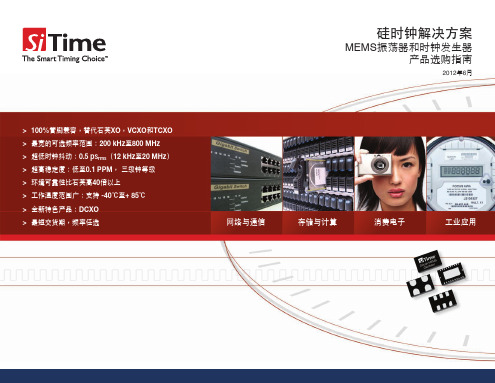
Sitime产品选型手册中文2012
p p
p p
-
p p
-
压控振荡器 — VCXO
SiT3807 网络、电信、 医疗、ATE、 视频、xDSL、 及嵌入式系统 VCXO • 可选标准频率,最大程度降低 成本 • 超低相位抖动: 0.5 psrms • 最广牵引范围 • 1%牵引线性度 • 超低相位抖动: 0.5 psrms 1.5-45 (标准频点范围) 1-80 10, 25, 50 80-220 25, 50 25-200 (1%线性度) CMOS LVTTL 32 70 µA (待机) C, I 2.5x2.0 mm 3.2x2.5 mm 5.0x3.2 mm 7.0x5.0 mm
-
-
要求低EMI的计算机 设备应用 应用、服务器
SiT9002
SSXO
• 扩频设计: 中心展频或向下 展频
1-220
25, 50
-
LVPECL LVDS HCSL CML
48-75
C, I
5.0x3.2 mm 7.0x5.0 mm
p
p
-
p
差分压控振荡器 — VCXO
SiT3821 网络、电信、 医疗、ATE、 视频、xDSL、 嵌入式系统 SiT3822 VCXO • 最佳稳定度 • 1%牵引线性度 • 超低相位抖动: 0.5 psrms 220-625 1-220 10, 25, 50 25-1600 (1% 牵引线 性度) LVPECL LVDS 55-69 C, I 5.0x3.2 mm 7.0x5.0 mm
单端数控振荡器 — DCXO
网络及电信
SiT3907
DCXO
• 单引脚串口可编程 • 0.1% 牵引线性度动 • 超低相位抖动 0.5 psrms
SY8008 SY8009 datasheet 规格书
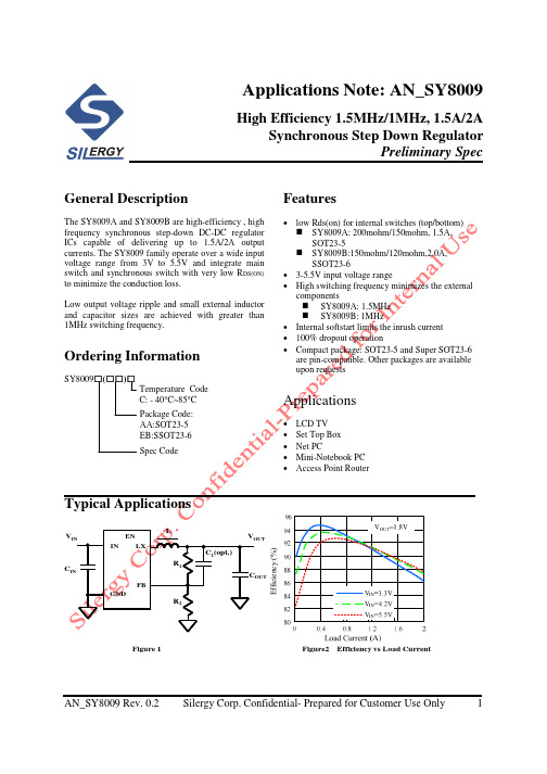
Applications Note: AN_SY8009High Efficiency 1.5MHz/1MHz, 1.5A/2A Synchronous Step Down Regulator Preliminary Spec General DescriptionThe SY8009A and SY8009B are high-efficiency , high frequency synchronous step-down DC-DC regulator ICs capable of delivering up to 1.5A/2A output currents. The SY8009 family operate over a wide input voltage range from 3V to 5.5V and integrate main switch and synchronous switch with very low RDS(ON) to minimize the conduction loss. Low output voltage ripple and small external inductor and capacitor sizes are achieved with greater than 1MHz switching frequency.Features• low Rds(on) for internal switches (top/bottom) SY8009A: 200mohm/150mohm, 1.5A, SOT23-5 SY8009B:150mohm/120mohm,2.0A, SSOT23-6 • 3-5.5V input voltage range • High switching frequency minimizes the external components SY8009A: 1.5MHz SY8009B: 1MHz • Internal softstart limits the inrush current • 100% dropout operation • Compact package: SOT23-5 and Super SOT23-6 are pin-compatible. Other packages are available upon requestsOrdering InformationSY8009□(□□ □ □ □□ □□)□ Temperature Code C: - 40°C~85°C Package Code: AA:SOT23-5 EB:SSOT23-6 Spec CodeApplications• • • • •LCD TV Set Top Box Net PC Mini-Notebook PC Access Point RouterTypical ApplicationsVININ EN LXL C1(opt.) R1VOUTCINFB GNDCOUT R2Figure 1Efficiency (%)Figure2Efficiency vs Load CurrentAN_SY8009 Rev. 0.2Silergy Corp. Confidential- Prepared for Customer Use Only1AN_SY8009Pinout (top view)(SY8009A, SOT23-5)(SY8009B, SSOT23-6)Top Mark: ADxyz for SY8009A , ASxyz for SY8009B (Device code: AD for SY8009A and AS for SY8009B, x=year code, y=week code, z= lot number code) Pin Name EN GND LX IN FB Pin Number 1 2 3 4 6(SSOT23-6) Pin Description Enable control. Pull high to turn on. Do not float. Ground pin Inductor pin. Connect this pin to the switching node of inductor. Input pin. Decouple this pin to GND pin with at least 1uF ceramic cap. Output Feedback Pin. Connect this pin to the center point of the output resistor divider (as shown in Figure 1) to program the output voltage: Vout=0.6*(1+R1/R2).Absolute Maximum Ratings (Note 1)Supply Input Voltage ------------------------------------------------------------------------------------------ 6.0V Enable, FB Voltage--------------------------------------------------------------------------------------------- VIN + 0.6V Power Dissipation, PD @ TA = 25°C ,SOT23-5,SSOT23-6 --------------------------------------------- 0.4W Package Thermal Resistance (Note 2) SOT23-5,SSOT23-6, θ JA --------------------------------------------------------------------------- 250°C/W SOT23-5,SSOT23-6, θ JC ----------------------------------------------------------------------------130°C/W Junction Temperature Range ----------------------------------------- -----------------------------------------150°C Lead Temperature (Soldering, 10 sec.) ---------------------------------------------------------------------- 260°C Storage Temperature Range ---------------------------------------------------------------------------------- -65°C to 150°C ESD Susceptibility (Note 2) HBM (Human Body Mode) ----------------------------------------------------------------------------------- 2kV MM (Machine Mode) ------------------------------------------------------------------------------------------ 200VRecommended Operating Conditions (Note 3)Supply Input Voltage ------------------------------------------------------------------------------------------3V to 5.5V Junction Temperature Range -------------------------------------------------------------------------------- -40°C to 125°C Ambient Temperature Range -------------------------------------------------------------------------------- -40°C to 85°CAN_SY8009 Rev. 0.2Silergy Corp. Confidential- Prepared for Customer Use Only2AN_SY8009Electrical Characteristics(VIN = 5V, VOUT = 2.5V, L = 2.2uH, COUT = 10uF, TA = 25°C, unless otherwise specified)Parameter Input Voltage Range Quiescent Current Shutdown Current Feedback Reference Voltage FB Input Current PFET RON NFET RON PFET Current Limit EN rising threshold EN falling threshold Input UVLO threshold UVLO hysteresis Oscillator Frequency Min ON Time Max Duty Cycle Thermal Shutdown TemperatureSymbol VIN IQ ISHDN VREF IFB RDS(ON),P RDS(ON),N ILIM VENH VENL VUVLO VHYS FOSCTest Conditions IOUT=0, VFB=VREF ⋅ 105% EN=0Min 3Typ 80 0.1 0.6Max 5.5 1 0.612 500.588 VFB=VIN SY8009A SY8009B SY8009A SY8009B SY8009A SY8009B -50Unit V µA µA V nA Ω Ω Ω Ω A A V V V V MHz MHz ns % °C0.2 0.15 0.15 0.12 1.8 2.5 1.5 0.4 1.8 0.1 1.5 1 50 100 160IOUT=200mA, SY8009A IOUT=500mA, SY8009BTSDNote 1: Stresses listed as the above “Absolute Maximum Ratings” may cause permanent damage to the device. These are for stress ratings. Functional operation of the device at these or any other conditions beyond those indicated in the operational sections of the specifications is not implied. Exposure to absolute maximum rating conditions for extended periods may remain possibility to affect device reliability. Note 2: θ JA is measured in the natural convection at TA = 25°C on a low effective single layer thermal conductivity test board of JEDEC 51-3 thermal measurement standard. Pin 2 of SOT23-5/SSOT-23-5 packages is the case position for θ JC measurement. Note 3: The device is not guaranteed to function outside its operating conditions.AN_SY8009 Rev. 0.2Silergy Corp. Confidential- Prepared for Customer Use Only3AN_SY8009Typical Performance Characteristics(SY8009B)Efficiency vs Load Current Efficiency vs Load Current Efficiency vs Load CurrentOutput Ripple(Vin=5.0V, Vout=1.8V,Iload=0.5A)Output Ripple(Vin=5.0V, Vout=1.8V,Iload=1.5A)Output Ripple(Vin=5.0V, Vout=1.8V,Iload=2A)Startup(Vin=5.0V, Vout=1.8V,Iload=2A)Shutdown(Vin=5.0V, Vout=1.8V,Iload=2A)Short Protection/Current limit(Vin=5.0V, Vout=1.8V,open to short)AN_SY8009 Rev. 0.2Silergy Corp. Confidential- Prepared for Customer Use Only4AN_SY8009Soft Start(Vo) Soft Start(Lx) Load Transient(Vin=5.0VmVout=1.8V,Iload=0~1A)Load Transient(Vin=5.0V, Vout=1.8V,Iload=0.2~2A)Case Temperature vs Output Current Oscillator Frequency vs Vin(Vin=5V,Vo=1.8V,Ta=27℃)AN_SY8009 Rev. 0.2Silergy Corp. Confidential- Prepared for Customer Use OnlyTC(°C)5AN_SY8009OperationSY8009 is a synchronous buck regulator IC that integrates the PWM control, top and bottom switches on the same die to minimize the switching transition loss and conduction loss. With ultra low Rds(on) power switches and proprietary PWM control, this regulator IC can achieve the highest efficiency and the highest switch frequency simultaneously to minimize the external inductor and capacitor size, and thus achieving the minimum solution footprint.Applications InformationBecause of the high integration in the SY8009 IC, the application circuit based on this regulator IC is rather simple. Only input capacitor CIN, output capaictor COUT, output inductor L and feedback resistors (R1 and R2) need to be selected for the targeted applications specifications. Feedback resistor dividers R1 and R2: Choose R1 and R2 to program the proper output voltage. To minimize the power consumption under light loads, it is desirable to choose large resistance values for both R1 and R2. A value of between 10k and 200k is highly recommended for R2. If R2=100k is chosen, then R1 can be calculated to be:R1 =(VOUT − 0.6 V) ⋅ R2 0.6VInput capacitor CIN:With the maximum load current at 1.2A, the maximum ripple current through input capacitor is about 0.6Arms. A typical X7R or better grade ceramic capacitor with 6V rating and greater than 4.7uF capacitance can handle this ripple current well. To minimize the potential noise problem, place this ceramic capacitor really close to the IN and GND pins. Care should be taken to minimize the loop area formed by CIN, and IN/GND pins. Output capacitor COUT: The output capacitor is selected to handle the output ripple noise requirements. Both steady state ripple and transient requirements must be taken into consideration when selecting this capacitor. For the best performance, it is recommended to use X7R or better grade ceramic capacitor with 6V rating and greater than 4.7uF capacitance. Output inductor L: There are several considerations in choosing this inductor. 1) Choose the inductance to provide the desired ripple current. It is suggested to choose the ripple current to be about 40% of the maximum output current. The inductance is calculated as: VOUT (1 − VOUT/VIN,MAX ) L= FSW × IOUT,MAX × 40% where Fsw is the switching frequency and IOUT,MAX is the maximum load current. The SY8009 regulator IC is quite tolerant of different ripple current amplitude. Consequently, the final choice of inductance can be slightly off the calculation value without significantly impacting the performance. 2) The saturation current rating of the inductor must be selected to be greater than the peak inductor current under full load conditions. VOUT(1-VOUT/VIN,MAX) ISAT, MIN > IOUT, MAX + 2 ⋅ FSW ⋅ L 3) The DCR of the inductor and the core loss at the switching frequency must be low enough to achieve the desired efficiency requirement. It is desirable to choose an inductor with DCR<50mohm to achieve a good overall efficiency. Layout Design: The layout design of SY8009 regulator is relatively simple. For the best efficiency and minimum noise problems, we should place the following components close to the IC: CIN, L, R1 and R2. 1) It is desirable to maximize the PCB copper area connecting to GND pin to achieve the best thermal and noise performance. If the board space allowed, a ground plane is highly desirable.AN_SY8009 Rev. 0.2Silergy Corp. Confidential- Prepared for Customer Use Only6AN_SY80092) CIN must be close to Pins IN and GND. The loop area formed by CIN and GND must be minimized. 3) The PCB copper area associated with LX pin must be minimized to avoid the potential noise problem. 4) The components R1 and R2, and the trace connecting to the FB pin must NOT be adjacent to the LX net on the PCB layout to avoid the noise problem. 5) If the system chip interfacing with the EN pin has a high impedance state at shutdown mode and the IN pin is connected directly to a power source such as a LiIon battery, it is desirable to add a pull down 1Mohm resistor between the EN and GND pins to prevent the noise from falsely turning on the regulator at shutdown mode. Load Transient Considerations: The SY8009 regulator IC integrates the compensation components to achieve good stability and fast transient responses. In some applications, adding a 22pF ceramic cap in parallel with R1 may further speed up the load transient responses and is thus recommended for applications with large load transient step requirements.AN_SY8009 Rev. 0.2Silergy Corp. Confidential- Prepared for Customer Use Only7AN_SY8009SOT23-5 Package outline & PCB layout design0.552.80 - 3.102.400.95 TYP0.802.70 - 3.000.30 - 0.50Recommended Pad Layout0.25 REF0.1 - 0.151.0 - 1.30.95 TYP0.3 - 0.61.90 TYPNotes: All dimensions are in millimeters. All dimensions don’t include mold flash & metal burr.AN_SY8009 Rev. 0.2Silergy Corp. Confidential- Prepared for Customer Use Only0.01 - 0.11.50 - 1.708AN_SY8009SSOT23-6 Package outline & PCB layout design1.901.002.30 - 2.500.950.600.25 - 0.40Recommended Pad Layout2.95 - 3.102.50 - 3.000.95 TYP 0.01 - 0.102.400.10 - 0.200.30 - 0.60Notes: All dimensions are in millimeters. All dimensions don’t include mold flash & metal burr.AN_SY8009 Rev. 0.2Silergy Corp. Confidential- Prepared for Customer Use Only0.90 - 1.009。
RT8008资料

Features
l l l
l l l l l l
+2.5V to +5.5V Input Range Adjustable Output From 0.6V to VIN 1.0V, 1.2V, 1.5V, 1.8V, 2.5V and 3.3V Fixed/ Adjustable Output Voltage 600mA Output Current, 1A Peak Current 95% Efficiency No Schottky Diode Required 1.5MHz Fixed-Frequency PWM Operation Small SOT-23-5 and TSOT-23-5 Package RoHS Compliant and 100% Lead (Pb)-Free
2
DS8008-04 March 2007
元器件交易网
RT8008
Functional Pin Description
Pin Number 1 2 3 4 5 Pin Name EN GND LX VIN FB/VOUT Pin Function Chip Enable (Active High, do not leave EN pin floating, and VEN < VIN + 0.6V). Ground. Pin for Switching. Power Input. Feedback Input Pin.
Note : RichTek Pb-free and Green products are :
Pin Configurations
(TOP VIEW)
EN GND LX 1 2 3 4 VIN 5 FB/VOUT
ATM8F8040 数据手册说明书
第1共13页页ATM8F8040数据手册版本号更新时间更新内容V1.02020-09-05V1.0正式版本发布V1.12020-09-16V1.1版本发布,修正DNL参数V1.22020-12-10统一数据手册和应用手册的关于T2CAP的描述V1.32021-3-1增加16脚SOP16封装信息V1.42021-3-8更新IDD2测试条件第2页1.主要特色CPU 特性通信8位1T 8051内核支持两路UART 支持1/2/4/8系统分频模拟模块支持双DPTR 支持12路12位ADC 支持双线调试支持上电复位ROM支持低压复位16K 字节FLASH(擦写寿命1000次)时钟128字节EEPROM(擦写寿命10000次)内部时钟频率最高到32MHz,1%精度数据保持时间:10年内部时钟32KHz 低频振荡器RAM支持外部1-20MHz 晶振256字节内部IRAM 工作模式512字节外部XRAM 正常模式GPIO待机模式(IDLE)最多支持18个GPIO 停机模式(Stop),最小电流<1uA 支持任意端口变化中断工作条件Timer/PWM工作频率:最大32MHz 16位8051标准定时器T0/T1工作电压: 2.7~5.5V 带捕获和可编程输出的16位定时器T2工作温度:-40℃~85℃7路16位带互补输出PWM 输出模块封装唤醒Timer 20-TSSOP 看门狗定时器20-QFN 4x4SOP16其他CRC16循环冗余检测模块可配置逻辑计算单元(CPL)外部晶振停振检测1.主要特色 (2)2.概述 (4)2.1.说明 (4)2.2.应用方向 (4)3.设计框图 (4)4.引脚分布图 (5)5.封装尺寸图 (7)5.1.20-TSSOP (7)5.2.20-QFN (8)5.3.SOP16 (9)6.电气特性 (10)6.1.极限参数 (10)6.2.DC特性 (10)6.3.ADC特性 (11)6.4.内部高频振荡器特性 (11)6.5.内部低频振荡器特性 (11)6.6.外部振荡器特性 (12)6.7.存储器工作特性 (12)6.8.外部复位及中断管脚特性 (12)7.芯片选型 (13)2.概述2.1.说明ATM8F8040是一款内嵌16K字节FLASH的8位单片机。
- 1、下载文档前请自行甄别文档内容的完整性,平台不提供额外的编辑、内容补充、找答案等附加服务。
- 2、"仅部分预览"的文档,不可在线预览部分如存在完整性等问题,可反馈申请退款(可完整预览的文档不适用该条件!)。
- 3、如文档侵犯您的权益,请联系客服反馈,我们会尽快为您处理(人工客服工作时间:9:00-18:30)。
Electrical Characteristics
All Min and Max limits are specified over temperature and rated operating voltage with 15 pF output load unless otherwise stated. Typical values are at 25°C and nominal supply voltage.
+50 ppm Operating Temperature Range +70 °C
Hale Waihona Puke – +85 °C Industrial Supply Voltage and Current Consumption 1.8 2.5 2.8 3.0 3.3 – 3.8 3.7 3.5 – – 2.1 1.1 1.98 2.75 3.08 3.3 3.63 3.63 4.5 4.2 4.1 4.2 4.0 4.3 2.5 V V V V V V mA mA mA mA mA A A Contact SiTime for 1.5V support
Table 2. Pin Description
Pin Symbol Output Enable 1 OE/ST/NC Standby No Connect 2 3 4 GND OUT VDD Power Output Power Functionality H[1]: specified frequency output L: output is high impedance. Only output driver is disabled. H[1]: specified frequency output L: output is low (weak pull down). Device goes to sleep mode. Supply current reduces to I_std. Any voltage between 0 and Vdd or Open[1]: Specified frequency output. Pin 1 has no function. Electrical ground Oscillator output Power supply voltage[2] OE/ST/NC
SiT8008B
Low Power Programmable Oscillator Features ow Power, Standard Frequency Oscillator
Applications
Any frequency between 1 MHz and 110 MHz accurate to 6 decimal places 100% pin-to-pin drop-in replacement to quartz-based XO Excellent total frequency stability as low as ±20 ppm Operating temperature from -40°C to 85°C. For 125°C and/or -55°C options, refer to SiT1618, SiT8918, SiT8920 Low power consumption of 3.5 mA typical at 1.8V Standby mode for longer battery life Fast startup time of 5 ms LVCMOS/HCMOS compatible output Industry-standard packages: 2.0 x 1.6, 2.5 x 2.0, 3.2 x 2.5, 5.0 x 3.2, 7.0 x 5.0 mm x mm Instant samples with Time Machine II and field programmable oscillators RoHS and REACH compliant, Pb-free, Halogen-free and Antimony-free For AEC-Q100 oscillators, refer to SiT8924 and SiT8925
1
Top View
4
VDD
GND
2
3
OUT
Figure 1. Pin Assignments
Notes: 1. In OE or ST mode, a pull-up resistor of 10 kΩ or less is recommended if pin 1 is not externally driven. If pin 1 needs to be left floating, use the NC option. 2. A capacitor of value 0.1 µF or higher between Vdd and GND is required.
Rev. 1.04
Page 2 of 17
SiT8008B Low Power Programmable Oscillator
Current Consumption
Idd
No load condition, f = 20 MHz, Vdd = 2.8V to 3.3V No load condition, f = 20 MHz, Vdd = 2.5V No load condition, f = 20 MHz, Vdd = 1.8V Vdd = 2.5V to 3.3V, OE = GND, Output in high-Z state Vdd = 1.8V, OE = GND, Output in high-Z state ST = GND, Vdd = 2.8V to 3.3V, Output is weakly pulled down ST = GND, Vdd = 2.5V, Output is weakly pulled down
Ideal for DSC, DVC, DVR, IP CAM, Tablets, e-Books, SSD, GPON, EPON, etc Ideal for high-speed serial protocols such as: USB, SATA, SAS, Firewire, 100M / 1G / 10G Ethernet, etc.
SiTime硅晶振样品中心 Rev. 1.0 4
SiTime中国区技术支持
SiT8008B Low Power Programmable Oscillator
Table 1. Electrical Characteristics (continued)
Parameters Input High Voltage Input Low Voltage Input Pull-up Impedance Symbol VIH VIL Z_in Min. 70% – 50 2 Startup Time Enable/Disable Time Resume Time RMS Period Jitter Peak-to-peak Period Jitter RMS Phase Jitter (random) T_start T_oe T_resume T_jitt T_pk T_phj – – – – – – – – – Typ. – – 87 Max. – 30% 150 Unit Vdd Vdd k Pin 1, OE or ST Pin 1, OE or ST Pin 1, OE logic high or logic low, or ST logic high Condition Input Characteristics
0.2 1.3 ST = GND, Vdd = 1.8V, Output is weakly pulled down A LVCMOS Output Characteristics – 1 1.3 – – – 55 2 2.5 2 – 10% % ns ns ns Vdd Vdd All Vdds. See Duty Cycle definition in Figure 3 and Footnote 6 Vdd = 2.5V, 2.8V, 3.0V or 3.3V, 20% - 80% Vdd =1.8V, 20% - 80% Vdd = 2.25V - 3.63V, 20% - 80% IOH = -4 mA (Vdd = 3.0V or 3.3V) IOH = -3 mA (Vdd = 2.8V and Vdd = 2.5V) IOH = -2 mA (Vdd = 1.8V) IOL = 4 mA (Vdd = 3.0V or 3.3V) IOL = 3 mA (Vdd = 2.8V and Vdd = 2.5V) IOL = 2 mA (Vdd = 1.8V)
– – Pin 1, ST logic low M Startup and Resume Timing – – – 1.8 1.8 12 14 0.5 1.3 5 130 5 Jitter 3 3 25 30 0.9 2 ps ps ps ps ps ps f = 75 MHz, Vdd = 2.5V, 2.8V, 3.0V or 3.3V f = 75 MHz, Vdd = 1.8V f = 75 MHz, Vdd = 2.5V, 2.8V, 3.0V or 3.3V f = 75 MHz, Vdd = 1.8V f = 75 MHz, Integration bandwidth = 900 kHz to 7.5 MHz f = 75 MHz, Integration bandwidth = 12 kHz to 20 MHz ms ns ms Measured from the time Vdd reaches its rated minimum value f = 110 MHz. For other frequencies, T_oe = 100 ns + 3 * cycles Measured from the time ST pin crosses 50% threshold