MSP430F_PCB图
msp430f449简介

1、低工作电压:1.8~3.6V 2、超低功耗: 活动模式:280UA(1MHZ,2.2V) 待机模式 : 1.1UA 掉电模式 :(RAM数据保持)0.1UA 3、有5种节电模式 4、从待机到唤醒的响应时间不超过6us 5、12位A/D转换器 (8通道、带有内部参考源、采样保持) 6、16位精简指令结构(RISC),150ns指令周期 7、带有3个捕获/比较器结构的16位定时器 8、串行通信可软件选择UART/SPI两种模式 9、可在线串行编程,不需要外部编程电压 10、驱动液晶能力为160段 11、FLASH存储器为60KB,RAM为2KB
3、如何选择 XT2CLK作为MCLK: void clk_initial() { do { IFG1&=~OFIFG; //清除振荡器的失效标志 __delay_cycles(200); } while((IFG1&OFIFG)!=0); //如果振荡器的失效标志存在 FLL_CTL1=SELM1; //选择XT2CLK作为MCLK } 4、如何选择 DCOCLK作为MCLK:计算(121+1)*2*32768=7.995MHZ void CLK_initial() { SCFI0|=FN_4; //选择DCO频率调整范围为2.8~26.6MHZ SCFQCTL=249; //倍频倍数,最高位为DCO+调制器的控制位 FLL_CTL0=DCOPLUS+OSCCAP_1; //选择DCO作为MCLK前分频 }
三、基本操作:
1、所有P口都可作为通用IO口使用 2、所有P口都可进行字节操作和位操作 按字节操作: 例 P1DIR=0xff; //将P1口作为输出口 PIOUT=0x20; // P1口输出0x20 P1DIR=0x00; //将P1口作为输入口 data=P1IN //读取P1口外部输入值 按位操作: 例 P1DIR=BIT0; //将P1.0作为输出口 P1OUT|=BIT0; //P1.0输出1 P1OUT&=~BIT0; //P1.0输出0 P1DIR&=~BIT0; //将P1.0口作为输入 data=P1IN&BIT0; //读取P1.0口外部输入值
msp430f5529引脚图
msp430f5529 引脚图
MSP430F5529 实验板(MSP-EXP430F5529)是一个用于MSP430F5529 器件(来自最新一代具有集成USB 的MSP430 器件)的开发平台。
该实验板与CC2520EMK 等众多TI 低功耗射频无线评估模块兼容。
该实验板能帮助设计者快速使用新的F55xx MCU 进行学习和开发,其中F55xx MCU 为能量收集、无线传感以及自动抄表基础设施(AMI)等
应用提供了业界最低工作功耗的集成USB、更大的内存和领先的集成技术。
该实验板上的MSP430F5529 器件可以通过集成ezFET 或通过TI 闪存仿真工具(如MSP-FET430UIF)进行供电和调试。
基于新的MSP430F5529 MCU,可用于需要增强型功能和集成USB 的超低功耗设计
凭借eZ430-RF2500 工具、用于Z-Stack Pro 的开包即用平台以及对各种TI 低功耗射频无线评估模块的支持,可实现快速的低功耗无线开发,
覆盖低于1GHz 和2.4GHz 的频带。
M430F4152单片机资料

DWake-Up From Standby Mode in Less Than 6µs --Internal Very Low Power,Low-Frequency Oscillator D 16-Bit RISC Architecture,125-ns Instruction Cycle Time D 16-Bit Timer_A With Three Capture/Compare RegistersD 16-Bit Timer_A With Five Capture/Compare RegistersDTwo Universal Serial Communication Interfaces (USCIs)USCI_A0--Enhanced UART Supporting Auto-Baudrate Detection --IrDA Encoder and Decoder --Synchronous SPI USCI_B0--I2C --Synchronous SPIDSupply Voltage Supervisor/Monitor With Programmable Level DetectionCompare Function or Slope A/DD10-Bit 200-ksps Analog-to-Digital (A/D)Converter With Internal Reference,Sample-and-Hold,Autoscan,and Data Transfer ControllerDSerial Onboard Programming,No External Programming Voltage Needed Programmable Code Protection by Security FuseD Bootstrap LoaderD On-Chip Emulation Module DFamily Members Include:MSP430F4152:16KB+256B Flash Memory512B RAMMSP430F4132:8KB+256B Flash Memory512B RAMD Available in 64-Pin QFP Package and 48-Pin QFN Package (See Available Options)DFor Complete Module Descriptions,See The MSP430x4xx Family User’s Guide ,Literature Number SLAU056descriptionThe Texas Instruments MSP430family of ultralow-power microcontrollers consist of several devices featuring different sets of peripherals targeted for various applications.The architecture,combined with five low power modes,is optimized to achieve extended battery life in portable measurement applications.The device features a powerful 16-bit RISC CPU,16-bit registers,and constant generator that contribute to maximum code efficiency.The digitally controlled oscillator (DCO)allows wake-up from low-power modes to active mode in less than 6µs.The MSP430F41x2is a microcontroller configuration with two 16-bit timers,a basic timer with a real--time clock,a 10-bit A/D converter,a versatile analog comparator,two universal serial communication interfaces,up to 48I/O pins,and a liquid crystal display driver.Typical applications for this device include analog and digital sensor systems,remote controls,thermostats,digital timers,hand-held meters,etc.This integrated circuit can be damaged by ESD.Texas Instruments recommends that all integrated circuits be handled with appropriate precautions.Failure to observe proper handling and installation procedures can cause damage.ESD damage can range from subtle performance degradation to complete device failure.Precision integrated circuits may be more susceptible to damage because very small parametric changes could cause the device not to meet its published specifications.These devices have limited built-in ESD protection.Please be aware that an important notice concerning availability,standard warranty,and use in critical applications of Texas Instruments semiconductor products and disclaimers thereto appears at the end of this data sheet.PRODUCTION DATA information is current as of publication date.Products conform to specifications per the terms of Texas Instruments standard warranty.Production processing does not necessarily include testing of all parameters.AVAILABLE OPTIONS†PACKAGED DEVICES‡T APLASTIC64-PIN QFP(PM)PLASTIC48-PIN QFN(RGZ)--40°C to85°C MSP430F4152IPMMSP430F4132IPMMSP430F4152IRGZMSP430F4132IRGZ†For the most current package and ordering information,see the Package OptionAddendum at the end of this document,or see the TI web site at .‡Package drawings,thermal data,and symbolization are available at/packaging.DEVELOPMENT TOOL SUPPORTAll MSP430microcontrollers include an Embedded Emulation Module(EEM)allowing advanced debugging and programming through easy to use development tools.Recommended hardware options include the following:D Debugging and Programming Interface--MSP-FET430UIF(USB)--MSP-FET430PIF(Parallel Port)D Debugging and Programming Interface with Target Board--MSP-FET430U64A(PM package)D Production Programmer--MSP-GANG430pin designation,MSP430F41x2IPM(QFP)pin designation,MSP430F41x2IRGZ(QFN)††“Not available”pinsfunctional block diagramDVCCDVSSAVCCAVSSP1.x/P2.xP3.x/P4.xXINXOUTP5.x/P6.xP7.xNOTE:The USCI A0and USCI B0cannot be used in the 48-pin package options (RGZ).Terminal FunctionsTERMINALNO.NAME64PIN 48PINI/O DESCRIPTIONP1.0/TA0.0/S315337I/O General-purpose digital I/O pinTimer0_A3,capture:CCI0A input,compare:Out0output LCD segment outputP1.1/TA0.0/MCLK/S305236I/O General-purpose digital I/O pin Timer0_A3,capture:CCI0B input MCLK signal outputLCD segment outputP1.2/TA0.1/S2951--I/O General-purpose digital I/O pinTimer0_A3,capture:CCI1A input,compare:Out1output LCD segment outputP1.3/TA1.0/SVSOUT/S2850--I/O General-purpose digital I/O pin Timer1_A5,capture:CCI0B input SVS comparator outputLCD segment outputP1.4/TA1.0/S2749--I/O General-purpose digital I/O pin/Timer1_A5,capture:CCI0A input,compare:Out0output LCD segment outputP1.5/TA0CLK/CAOUT/S264835I/O General-purpose digital I/O pin Timer0_A3,clock signal TACLK input Comparator_A outputLCD segment outputP1.6/ACLK/CA04734I/O General-purpose digital I/O pin Comparator_A input0ACLK signal outputP1.7/TA0CLKCAOUT/CA14633I/O General-purpose digital I/O pin Timer0_A3,clock signal TACLK input Comparator_A output Comparator_A input1P2.0/TA1.1/S152723I/O General-purpose digital I/O pin Timer1_A5,compare:Out1Output LCD segment outputP2.1/TA1.2/S142622I/O General-purpose digital I/O pin Timer1_A5,compare:Out2Output LCD segment outputP2.2/TA1.3/S132521I/O General-purpose digital I/O pin Timer1_A5,compare:Out3Output LCD segment outputP2.3/TA1.4/S122420I/O General-purpose digital I/O pin Timer1_A5,compare:Out4output LCD segment outputP2.4/S112319I/O General-purpose digital I/O pin LCD segment outputP2.5/S102218I/O General-purpose digital I/O pin LCD segment outputP2.6/S92117I/O General-purpose digital I/O pin LCD segment outputP2.7/S82016I/O General-purpose digital I/O pin LCD segment outputTerminal Functions(continued)TERMINALNO.NAME64PIN 48PINI/O DESCRIPTIONP3.0/TA1.2/S2335--I/O General-purpose digital I/O pinTimer1_A5,capture:CCI2A input,compare:Out2output LCD segment outputP3.1/TA1.3/S2234--I/O General-purpose digital I/O pinTimer1_A5,capture:CCI3A input,compare:Out3output LCD segment outputP3.2/TA1.4/S2133--I/O General-purpose digital I/O pinTimer1_A5,capture:CCI4A input,compare:Out4output LCD segment outputP3.3/TA0.0/TA1CLK/S2032--I/O General-purpose digital I/O pin Timer0_A3,compare:Out0output Timer1_A5,clock signal TACLK input LCD segment outputP3.4/CAOUT/S193124I/O General-purpose digital I/O pin Comparator_A outputLCD segment outputP3.5/S1830--I/O General-purpose digital I/O pin LCD segment outputP3.6/S1729--I/O General-purpose digital I/O pin LCD segment outputP3.7/S1628--I/O General-purpose digital I/O pin LCD segment outputP4.0/S71915I/O General-purpose digital I/O pin LCD segment outputP4.1/S61814I/O General-purpose digital I/O pin LCD segment outputP4.2/S51713I/O General-purpose digital I/O pin LCD segment outputP4.3/S41612I/O General-purpose digital I/O pin LCD segment outputP4.4/S31511I/O General-purpose digital I/O pin LCD segment outputP4.5/S21410I/O General-purpose digital I/O pin LCD segment outputP4.6/S1139I/O General-purpose digital I/O pin LCD segment outputP4.7/ADC10CLK/S0128I/O General-purpose digital I/O pin ADC10,conversion clock LCD segment outputP5.0/TA1.1/S2444--I/O General-purpose digital I/O pinTimer1_A5,capture:CCI1A input,compare:Out1output LCD segment outputLCDCAP/R334332I/O Capacitor connection for LCD charge pumpinput port of the most positive analog LCD level(V4)P5.1/R234231I/O General-purpose digital I/O pininput port of the second most positive analog LCD level(V3)P5.2/LCDREF/R134130I/O General-purpose digital I/O pinExternal LCD reference voltage inputinput port of the third most positive analog LCD level(V3or V2)Terminal Functions(continued)TERMINALNO.NAME64PIN 48PINI/O DESCRIPTIONP5.3/R034029I/O General-purpose digital I/O pininput port of the fourth most positive analog LCD level(V1)P5.4/COM33928I/O General-purpose digital I/O pincommon output,COM0--3are used for LCD backplanesP5.5/COM23827I/O General-purpose digital I/O pincommon output,COM0--3are used for LCD backplanesP5.6/COM13726I/O General-purpose digital I/O pincommon output,COM0--3are used for LCD backplanesP5.7/COM03625I/O General-purpose digital I/O pincommon output,COM0--3are used for LCD backplanesP6.0/TA1.2/A2†/CA46347I/O General-purpose digital I/O pin Timer1_A5,compare:Out2output ADC10analog input A2†Comparator_A input4P6.1/UCB0SOMI†/ UCB0SCL†11I/OGeneral-purpose digital I/O pinUSCI B0slave out/master in in SPI mode,SCL I2C clock in I2C mode†P6.2/UCB0SIMO†/ UCB0SDA†22I/OGeneral-purpose digital I/O pinUSCI B0slave in/master out in SPI mode,SDA I2C data in I2C mode†P6.3/UCB0STE/UCA0CLK/A3/ CA5/V eref--/V ref--3--I/OGeneral-purpose digital I/O pinUSCI B0slave transmit enable/USCI A0clock input/outputADC10analog input A3/negative referenceComparator_A input5P6.4/UCB0CLK/UCA0STE/A4/ CA6/V eref+/V ref+4--I/OGeneral-purpose digital I/O pinUSCI B0clock input/output,USCI A0slave transmit enableADC10analog input A4/positive referenceComparator_A input6P6.5/UCA0RXD/UCA0SOMI/A55--I/O General-purpose digital I/O pinUSCI A0receive data input in UART mode,slave data out/master in in SPI mode ADC10analog input A5P6.6/UCA0TXD/UCA0SIMO/A66--I/O General-purpose digital I/O pinUSCI A0transmit data output in UART mode,slave data in/master out SPI mode ADC10analog input A6P6.7/A7/CA7/SVSIN117I/O General-purpose digital I/O pin ADC10analog input A7 Comparator_A input7SVS inputP7.0/TDO/TDI/ S325438I/O General-purpose digital I/O pinJTAG test data output terminal or test data input in programming an testLCD segment outputP7.1/TDI/TCLK/ S335539I/O General-purpose digital I/O pinJTAG test data input or test clock input in programming an testLCD segment outputP7.2/TMS/S345640I/O General-purpose digital I/O pinJTAG test mode select,input terminal for device programming and testLCD segment output64-pin package devices onlyTerminal Functions(continued)TERMINALNO.NAME64PIN 48PINI/O DESCRIPTIONP7.3/TCK/S355741I/O General-purpose digital I/O pinTest clock input for device programming and testLCD segment outputP7.4/TA1.4/A0/CA26044I/O General-purpose digital I/O pinTimer1_A5,capture:CCI4B input,compare:Out4output ADC10analog input A0Comparator_A input2P7.5/TA1.3/A1/CA36145I/O General-purpose digital I/O pinTimer1_A5,capture:CCI3B input,compare:Out3output ADC10analog input A1Comparator_A input3P7.6/TA0.2/S2545--I/O General-purpose digital I/O pinTimer0_A3,capture:CCI2A input,compare:Out2output LCD segment outputAV CC6448Analog supply voltage,positive terminalAV SS6246Analog supply voltage,negative terminalDV CC73Digital supply voltage,positive terminal.Supplies all digital parts.DV SS106Digital supply voltage,negative terminal.Supplies all digital parts.XOUT95O Output port for crystal oscillator XT1.Standard or watch crystals can be connected. XIN84I Input port for crystal oscillator XT1.Standard or watch crystals can be connected.RST/NMI/ SBWTDIO 5842I Reset or nonmaskable interrupt inputSpy-Bi-Wire test data input/output during programming and testTEST/SBWTCLK5943I Selects test mode for JTAG pins on Port7.The device protection fuse is connected to TEST. Thermal Pad NA NA NA QFN package pad(RGZ package only).Connection to DV SS is recommended.General-Purpose Register Program Counter Stack Pointer Status Register Constant Generator General-Purpose Register General-Purpose Register General-Purpose Register PC/R0SP/R1SR/CG1/R2CG2/R3R4R5R12R13General-Purpose Register General-Purpose Register R6R7General-Purpose Register General-Purpose Register R8R9General-Purpose Register General-Purpose Register R10R11General-Purpose Register General-Purpose RegisterR14R15short-form descriptionCPUThe MSP430CPU has a 16-bit RISC architecture that is highly transparent to the application.All operations,other than program-flow instructions,are performed as register operations in conjunction with seven addressing modes for source operand and four addressing modes for destination operand.The CPU is integrated with 16registers that provide reduced instruction execution time.The register-to-register operation execution time is one cycle of the CPU clock.Four of the registers,R0to R3,are dedicated as program counter,stack pointer,status register,and constant generator,respectively.The remaining registers are general-purpose registers.Peripherals are connected to the CPU using data,address,and control buses and can be handled with all instructions.instruction setThe instruction set consists of 51instructions with three formats and seven address modes.Each instruction can operate on word and byte data.Table 1shows examples of the three types of instruction formats;Table 2shows the address modes.Table 1.Instruction Word FormatsDual operands,source-destination e.g.,ADD R4,R5R4+R5------>R5Single operands,destination only e.g.,CALL R8PC ---->(TOS),R8---->PC Relative jump,un/conditionale.g.,JNEJump-on-equal bit =0Table 2.Address Mode DescriptionsADDRESS MODES D SYNTAX EXAMPLE OPERATION Register F F MOV Rs,Rd MOV R10,R11R10—>R11IndexedF F MOV X(Rn),Y(Rm)MOV 2(R5),6(R6)M(2+R5)—>M(6+R6)Symbolic (PC relative)F F MOV EDE,TONI M(EDE)—>M(TONI)Absolute F F MOV &MEM,&TCDAT M(MEM)—>M(TCDAT)Indirect F MOV @Rn,Y(Rm)MOV @R10,Tab(R6)M(R10)—>M(Tab+R6)Indirect autoincrement F MOV @Rn+,Rm MOV @R10+,R11M(R10)—>R11R10+2—>R10ImmediateFMOV #X,TONIMOV #45,TONI #45—>M(TONI)NOTE:S =source,D =destinationoperating modesThe MSP430has one active mode and five software selectable low-power modes of operation.An interrupt event can wake up the device from any of the five low-power modes,service the request,and restore back to the low-power mode on return from the interrupt program.The following six operating modes can be configured by software:D Active mode(AM)--All clocks are activeD Low-power mode0(LPM0)--CPU is disabled--ACLK and SMCLK remain active--FLL+loop control remains activeD Low-power mode1(LPM1)--CPU is disabled--ACLK and SMCLK remain active--FLL+loop control is disabledD Low-power mode2(LPM2)--CPU is disabled--MCLK,FLL+loop control,and DCOCLK are disabled--DCO’s dc generator remains enabled--ACLK remains activeD Low-power mode3(LPM3)--CPU is disabled--MCLK,FLL+loop control,and DCOCLK are disabled--DCO’s dc generator is disabled--ACLK remains activeD Low-power mode4(LPM4)--CPU is disabled--ACLK is disabled--MCLK,FLL+loop control,and DCOCLK are disabled--DCO’s dc generator is disabled--Crystal oscillator is stoppedinterrupt vector addressesThe interrupt vectors and the power-up starting address are located in the address range0xFFFF to0xFFC0.The vector contains the16-bit address of the appropriate interrupt-handler instruction sequence.If the reset vector(located at address0xFFFE)contains0xFFFF(e.g.,flash is not programmed),the CPU goes into LPM4immediately after power-up.INTERRUPT SOURCE INTERRUPT FLAG SYSTEM INTERRUPTWORDADDRESS PRIORITYPower-UpExternal ResetWatchdogFlash MemoryPC Out--of--Range(see Note4)PORIFGRSTIFGWDTIFGKEYV(see Note1)Reset0xFFFE15,highestNMIOscillator FaultFlash Memory Access ViolationNMIIFG(see Notes1and3)OFIFG(see Notes1and3)ACCVIFG(see Notes1,2,and4)(Non)maskable(Non)maskable(Non)maskable0xFFFC14Timer_A5TA1CCR0CCIFG0(see Note2)Maskable0xFFFA13Timer_A5TA1CCR1to TACCR4CCIFGs,and TAIFG(see Notes1and2)Maskable0xFFF812Comparator_A+CAIFG Maskable0xFFF611 Watchdog Timer+WDTIFG Maskable0xFFF410USCI_A0/B0ReceiveUCA0RXIFG(see Note1),UCB0RXIFG(SPI mode),orUCB0STAT UCALIFG,UCNACKIFG,UCSTTIFG,UCSTPIFG(I2C mode)(see Note1)Maskable0xFFF29USCI_A0/B0TransmitUCA0TXIFG(see Note1),UCB0TXIFG(SPI mode),orUCB0RXIFG and UCB0TXIFG(I2C mode)(see Note1)Maskable0xFFF08ADC10ADC10IFG(see Note2)Maskable0xFFEE7 Timer_A3TACCR0CCIFG0(see Note2)Maskable0xFFEC6Timer_A3TACCR1CCIFG1and TACCR2CCIFG2,TAIFG(see Notes1and2)Maskable0xFFEA5I/O Port P1(Eight Flags)P1IFG.0to P1IFG.7(see Notes1and2)Maskable0xFFE840xFFE630xFFE42 I/O Port P2(Eight Flags)P2IFG.0to P2IFG.7(see Notes1and2)Maskable0xFFE21 Basic Timer1/RTC BTIFG Maskable0xFFE00,lowest NOTES: 1.Multiple source flags2.Interrupt flags are located in the module.3.A reset is generated if the CPU tries to fetch instructions from within the module register memory address range(0h to01FFh).(Non)maskable:the individual interrupt-enable bit can disable an interrupt event,but the general-interrupt enable cannot disable it.4.Access and key violations,KEYV and ACCVIFG.special function registersMost interrupt and module-enable bits are collected in the lowest address space.Special-function register bits not allocated to a functional purpose are not physically present in the device.This arrangement provides simple software access.interrupt enable1and2Address7654321000h ACCVIE NMIIE OFIE WDTIEWDTIE Watchdog timer interrupt enable.Inactive if watchdog mode is selected.Active if watchdog timer is configured in interval timer mode.OFIE Oscillator fault enableNMIIE(Non)maskable interrupt enableACCVIE Flash access violation interrupt enableAddress7654321001h BTIE UCB0TXIE UCB0RXIE UCA0TXIE UCA0RXIEUCA0RXIE USCI_A0receive interrupt enableUCA0TXIE USCI_A0transmit interrupt enableUCB0RXIE USCI_B0receive interrupt enableUCB0TXIE USCI_B0transmit interrupt enableBTIE Basic timer interrupt enableinterrupt flag register1and2Address7654321002h NMIIFG RSTIFG PORIFG OFIFG WDTIFGrw--0rw--(0)rw--(1)rw--1rw--(0) WDTIFG Set on watchdog timer overflow(in watchdog mode)or security key violation.Reset on V CC power-up or a reset condition at RST/NMI pin in reset mode.OFIFG Flag set on oscillator faultRSTIFG External reset interrupt flag.Set on a reset condition at RST/NMI pin in reset mode.Reset on V CC power-up.PORIFG Power-on interrupt flag.Set on V CC power--up.NMIIFG Set via RST/NMI-pinAddress7654321003h BTIFG UCB0TXIFG UCB0RXIFGUCA0TXIFGUCA0RXIFGUCA0RXIFG USCI_A0receive interrupt flag UCA0TXIFG USCI_A0transmit interrupt flag UCB0RXIFG USCI_B0receive interrupt flag UCB0TXIFG USCI_B0transmit interrupt flag BTIFG Basic Timer1interrupt flagLegend rw:rw-0,1:Bit can be read and written.Bit can be read and written.It is Reset or set by PUC. Bit can be read and written.It is Reset or set by POR.rw-(0,1):SFR bit is not present in devicememory organizationMSP430F4152MSP430F4132MemoryMain:interrupt vector Main:code memorySizeFlashFlash16KB0FFFFh--0FFE0h0FFFFh--0C000h8KB0FFFFh--0FFE0h0FFFFh--0E000hInformation memory SizeFlash256Byte010FFh--01000h256Byte010FFh--01000hBoot memory SizeROM1KB0FFFh--0C00h1KB0FFFh--0C00hRAM Size512B03FFh--0200h512B03FFh--0200hPeripherals16-bit8-bit8-bit SFR 01FFh--0100h0FFh--010h0Fh--00h01FFh--0100h0FFh--010h0Fh--00hbootstrap loader(BSL)The MSP430BSL enables users to program the flash memory or RAM using a UART serial interface.Access to the MSP430memory via the BSL is protected by user-defined password.For complete description of the features of the BSL and its implementation,see the MSP430Memory Programming User’s Guide,literature number SLAU265.BSL FUNCTION PM PACKAGE PINS RGZ PACKAGE PINSData transmit53--P1.037--P1.0Data receive52--P1.136--P1.1flash memory(Flash)The flash memory can be programmed via the JTAG port,the bootstrap loader,or in-system by the CPU.The CPU can perform single-byte and single-word writes to the flash memory.Features of the flash memory include:D Flash memory has n segments of main memory and four segments of information memory(A to D)of64bytes each.Each segment in main memory is512bytes in size.D Segments0to n may be erased in one step,or each segment may be individually erased.D Segments A to D can be erased individually,or as a group with segments0to n.Segments A to D are also called information memory.peripheralsPeripherals are connected to the CPU through data,address,and control buses and can be handled using all instructions.For complete module descriptions,see the MSP430x4xx Family User’s Guide,literature number SLAU056.oscillator and system clockThe clock system in the MSP430F41x2is supported by the FLL+module that includes support for a32768-Hz watch crystal oscillator,an internal very low-power low--frequency oscillator,an internal digitally-controlled oscillator(DCO),and an8-MHz high-frequency crystal oscillator(XT1).The FLL+clock module is designed to meet the requirements of both low system cost and low power consumption.The FLL+features a digital frequency locked loop(FLL)hardware that,in conjunction with a digital modulator,stabilizes the DCO frequency to a programmable multiple of the watch crystal frequency.The internal DCO provides a fast turn-on clock source and stabilizes in less than6µs.The FLL+module provides the following clock signals:D Auxiliary clock(ACLK),sourced from a32768-Hz watch crystal,a high-frequency crystal,or a verylow-power LF oscillatorD Main clock(MCLK),the system clock used by the CPUD Sub-Main clock(SMCLK),the sub-system clock used by the peripheral modulesD ACLK/n,the buffered output of ACLK,ACLK/2,ACLK/4,or ACLK/8brownout,supply voltage supervisorThe brownout circuit is implemented to provide the proper internal reset signal to the device during power on and power off.The supply voltage supervisor(SVS)circuitry detects if the supply voltage drops below a user selectable level and supports both supply voltage supervision(the device is automatically reset)and supply voltage monitoring(SVM,the device is not automatically reset).The CPU begins code execution after the brownout circuit releases the device reset.However,V CC may not have ramped to V CC(min)at that time.The user must insure the default FLL+settings are not changed until V CC reaches V CC(min).If desired,the SVS circuit can be used to determine when V CC reaches V CC(min).digital I/OThere are seven8-bit I/O ports implemented—ports P1through P7.Port P7is a7-bit I/O port.D All individual I/O bits are independently programmable.D Any combination of input,output,and interrupt conditions is possible.D Edge-selectable interrupt input capability for all the eight bits of ports P1and P2.D Read/write access to port-control registers is supported by all instructions.watchdog timer (WDT+)The primary function of the WDT+module is to perform a controlled system restart after a software problem occurs.If the selected time interval expires,a system reset is generated.If the watchdog function is not needed in an application,the module can be configured as an interval timer and can generate interrupts at selected time intervals.Basic Timer1and Real-Time Clock (RTC)The Basic Timer1has two independent 8-bit timers which can be cascaded to form a 16-bit timer/counter.Both timers can be read and written by software.The Basic Timer1is extended to provide an integrated real-time clock (RTC).An internal calendar compensates for month with less than 31days and includes leap year correction.LCD_A driver with regulated charge pumpThe LCD_A driver generates the segment and common signals required to drive an LCD display.The LCD_A controller has dedicated data memory to hold segment drive mon and segment signals are generated as defined by the mode.Static,2--MUX,3--MUX,and 4--MUX LCDs are supported by this peripheral.The module can provide a LCD voltage independent of the supply voltage via an integrated charge pump.Furthermore it is possible to control the level of the LCD voltage and thus contrast in software.Timer0_A3Timer_A3is a 16-bit timer/counter with three capture/compare registers.Timer_A3can support multiple capture/compares,PWM outputs,and interval timing.Timer_A3also has extensive interrupt capabilities.Interrupts may be generated from the counter on overflow conditions and from each of the capture/compare registers.TIMER_A3SIGNAL CONNECTIONSINPUT PIN NUMBER DEVICE MODULE MODULE MODULE OUTPUT PIN NUMBER PM RGZ INPUTSIGNALINPUT NAMEBLOCKOUTPUT SIGNALPMRGZ48--P1.546--P1.735--P1.533--P1.7TA0CLK TACLK ACLK ACLK SMCLKSMCLK TimerNA48--P1.535--P1.5TA0CLK TACLK 53--P1.037--P1.0TA0.0CCI0A 53--P1.037--P1.052--P1.136--P1.1TA0.0CCI0B 32--P3.3--DV SS GND CCR0TA0DV CCV CC 51--P1.2--TA0.1CCI1A 51--P1.2CAOUT (internal)CCI1B ADC10(internal)ADC10(internal)DV SS GND CCR1TA1DV CCV CC 45--P7.6--TA0.2CCI2A 45--P7.6--ACLK (internal)CCI2B DV SS GND CCR2TA2DV CCV CCTimer1_A5Timer_A5is a 16-bit timer/counter with five capture/compare registers.Timer_A5can support multiple capture/compares,PWM outputs,and interval timing.Timer_A5also has extensive interrupt capabilities.Interrupts may be generated from the counter on overflow conditions and from each of the capture/compare registers.TIMER_A5SIGNAL CONNECTIONSINPUT PIN NUMBER DEVICE MODULE MODULE MODULE OUTPUT PIN NUMBER PM RGZ INPUTSIGNALINPUT NAMEBLOCKOUTPUT SIGNALPMRGZ32--P3.3--TA1CLK TACLK ACLK ACLK SMCLKSMCLK TimerNA32--P3.3--TA1CLK TACLK 49--P1.4--TA1.0CCI0A 49--P1.4--50--P1.3--TA1.0CCI0B ADC10(internal)ADC10(internal)DV SS GND CCR0TA0DV CCV CC 44--P5.0--TA1.1CCI1A 44--P5.0--CAOUT (internal)CCI1B 27--P2.023--P2.0DV SS GND CCR1TA1ADC10(internal)ADC10(internal)DV CCV CC 35--P3.0--TA1.2CCI2A 35--P3.0--ACLK (internal)CCI2B 26--P2.122--P2.1DV SS GND CCR2TA263--P6.047--P6.0DV CCV CC 34--P3.1--TA1.3CCI3A 34--P3.1--61--P7.545--P7.5TA1.3CCI3B 25--P2.221--P2.2DV SS GND CCR3TA361--P7.545--P7.5DV CCV CC 33--P3.2--TA1.4CCI4A 33--P3.2--60--P7.444--P7.4TA1.4CCI4B 24--P2.320--P2.3DV SS GND CCR4TA460--P7.444--P7.4DV CCV CCuniversal serial communication interface (USCI)(USCI_A0,USCI_B0)The USCI module is used for serial data communication.The USCI module supports synchronous communication protocols like SPI (3or 4pin),I2C and asynchronous communication protocols like UART,enhanced UART with automatic baudrate detection (LIN),and IrDA.USCI_A0provides support for SPI (3or 4pin),UART,enhanced UART,and CI_B0provides support for SPI (3or 4pin)and I2C.Comparator_A+The primary function of the comparator_A+module is to support precision slope analog-to-digital conversions,battery-voltage supervision,and monitoring of external analog signals.。
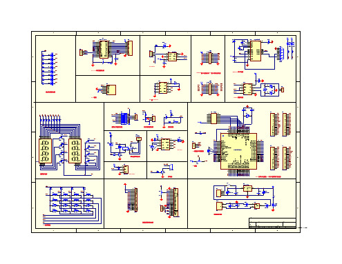
MSP430开发板原理图
R9 000
AVSS
1 AVcc DVss AVss P6.2/A2 P6.1/A1 P6.0/A0 RST/NMI TCK TMS TDI TDO/TDI XT2IN XT2OUT P5.7/TBoutH/SVSOUT P5.6/ACLK P5.5/SMCLK
P4.0 a b c d e f g dp R31 1K Q6 8550 R32 1K
1 2 3 4 5 6 7 8 9 10 11 12 13 14 15 16 17 18 19 20
VSS VCC V0 RS(CS) R/W(SID) E(SCLK) DB0 DB1 DB2 DB3 DB4 DB5 DB6 DB7 PSB NC RESET NC LED+ VSS 12864-ST7920
GND AVSS P6.2 P6.1 P6.0 RST TCK TMS TDI TDO XT2IN XT2OUT P5.7 P5.6 P5.5
com1 com2 com3 com4
蜂鸣器
P1.5 P1.6 P1.7 P2.0 P2.1 P2.2 P2.3 P2.4 P2.5 P2.6 P2.7 P3.0 P3.1 P3.2 P3.3 P3.4
AD采集
M 主芯片电路及430各个引脚的扩展电路 CU
A1 KEY D14
U8 LM1117-3.3V 3.3V 3 OUT 2 C5 104 R40 1K C12 10UF/16V
D13
5V
D20 + DC 2 1 C19 47UF/25V C20 104 1N4007 2 3
U5 GND OUT IN 78M05 D21 1 1N4007 D16 LED A
1 3 4 5 6 7 8 9 10 11 12 13 14 15 16
简易智能电动车 毕业设计

毕业设计(论文)中文摘要简易智能电动车摘要:本小车以MSP超低功耗单片机系列MSP430F149和MSP430FE425为核心,完成寻迹、检测金属、避障、寻光、测速等功能。
在机械结构上,对普通的小车作了改进,即用一个万用轮来代替两个前轮,使小车的转向更加灵敏。
采用PWM 驱动芯片控制电机,红外传感器检测黑线,金属传感器检测铁片,光敏器件检测光强,红外LED和一体化接收头来避障。
基于可靠的硬件设计和稳定的软件算法,实现题目要求。
而且附加实现显示起跑距离、行驶时间、检测金属数目等扩展功能。
关键词:MSP430 寻迹检测金属避障寻光毕业设计(论文)外文摘要Title: Simple Intelligent CarAbstract: This design is controlled with the MCU(MSP430F149,MSP430FE425) to complete the function of finding trace, detecting medal, avoiding barrier, tending to light and measure speed. By using infrared sensor to locate the trace、photoelectricity sense to measure the light、metal sensor to detect the metal and ultrasonic wave sensor to avoid the barrier. Based on the reliable hardware and software designing,this design is well fulfilled. In addition, such extended functions as measuring thedistance and recording the running-time are completed well. On the level of machine structure, we use a perfect wheel to make the car turning more convenience.Key words:MSP430 find trace detect medal avoid barrier and tend to light目录1 引言 (4)2 系统设计 (4)2.1 设计要求 (4)2.1.1 基本要求 (4)2.1.2发挥部分 (4)2.2方案论证与比较 (5)2.2.1电机驱动方案的选择与论证 (5)2.2.2路面寻线模块 (5)2.2.3金属检测模块 (5)2.2.4寻光模块 (5)2.2.5避障模块 (5)3硬件电路设计 (6)3.1 主控制模块 (6)3.2 电机驱动模块 (8)3.3 寻迹模块 (9)3.4 金属检测模块 (11)3.5 寻光避障模块 (11)3.6 测距和显示模块 (12)3.7电源模块 (13)4软件设计 (14)4.1 寻迹算法 (14)4.2 寻光,避障算法 (16)4.3串口通信 (20)5.系统测试 (22)5.1测试用仪表: (22)5.2测试数据: (22)结论 (23)致谢 (23)参考文献 (23)附录 (24)附件1:使用TI芯片 (24)附件2:元器件清单 (24)附件3:实物及PCB 图片 (25)1 引言随着素质教育的越来越被重视,很多学校都把制作智能小车作为首选课题,智能小车有趣生动并且还牵扯到机械结构、电子基础、传感器原理、自动控制、单片机、编程等诸多学科知识,学生通过动手实践能大大提高解决实际问题的能力,而且智能小车还是一个很好的硬件平台,只要增加一些控制电路就能完成循迹小车,机器人等课题。
MSP430电路图集锦
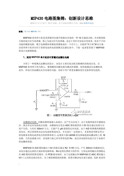
MSP430电路图集锦:创新设计思维2014年11月12日10:11 来源:电子发烧友网整合作者:Dick 我要评论(0)标签:TI(566)MSP430(499)MSP430系列单片机是美国德州仪器开始推向市场的一种16位超低功耗、具有精简指令集的混合信号处理器。
称之为混合信号处理器,是由于其针对实际应用需求,将多个不同功能的模拟电路、数字电路模块和微处理器集成在一个芯片上,以提供“单片机”解决方案。
该系列单片机多应用于需要电池供电的便携式仪器仪表中。
下面一起来看看基于MSP430的设计电路图集锦。
1、采用MSP430单片机的可穿戴式血糖仪电路介绍了一种便携式血糖仪的设计。
该设计主要从低功耗及精确性的角度出发,以MSP430系列单片机为核心,葡萄糖氧化酶电极为测试传感器,较快地测试出血糖浓度。
此外,所设计的血糖仪还具有储存功能,有助于用户查看血糖浓度历史值和变化趋势。
血糖测试电路:在酶电极两端滴入血液后,会产生自由电子。
由于电极两端存在激励电压,就会有定向电流流过电极。
该激励电压是由ADC模块提供的1.5V稳压通过电阻分压而产生的,大约在300mV左右,它能产生μA级别的定向电流。
由于A/D转换模块测量的是电压,所以需要将该定向电流转换成电压,并且进行一定的放大。
本系统采用图2所示的电路来实现电流到电压的转换和放大。
运算放大器LM358的反相端连接血糖试纸上的酶电极,当有血液滴入时,该电极与地之间为等效电阻Rx,流过该电阻的电流正比于血液中的血糖浓度值。
MSP430的A/D模块输出1.5V的稳压通过R2 和R3分压,产生300mV的激励电压,该电压通过运放的正端加到电极两端。
R4起到反馈放大的作用,它将运放的输出范围限定在A/D模块的转换范围内。
在PCB板布线时,由于运放输出和MSP430的ADC模块输入I/O口之间的走线比较长,为了确保测量值的准确,需要对测试电压进行滤波,C21就是用来起滤波作用的,以减少走线过长所引入的外来干扰对血糖测试的影响。
MSP430F149数据手册_引脚图_参数

An IMPORTANT NOTICE at the end of this data sheet addresses availability,warranty,changes,use in safety-critical applications,intellectual property matters and other important disclaimers.PRODUCTION DATA.MSP430F149,MSP430F148,MSP430F147MSP430F1491,MSP430F1481,MSP430F1471MSP430F135,MSP430F133SLAS272H –JULY 2000–REVISED MAY 20181Device Overview1.1Features•Low Supply Voltage Range,1.8V to 3.6V •Ultra-Low Power Consumption:–Active Mode:280µA at 1MHz,2.2V –Standby Mode:1.6µA–Off Mode (RAM Retention):0.1µA •Five Power-Saving Modes•Wakeup From Standby Mode in Less Than 6µs •16-Bit RISC Architecture,125-ns Instruction Cycle Time•12-Bit Analog-to-Digital Converter (ADC)With Internal Reference,Sample-and-Hold,and Autoscan Feature•16-Bit Timer_B With Seven Capture/Compare-With-Shadow Registers•16-Bit Timer_A With Three Capture/Compare Registers•On-Chip Comparator•Serial Onboard Programming,No External Programming Voltage Needed,Programmable Code Protection by Security Fuse•Serial Communication Interface (USART),Functions as Asynchronous UART or Synchronous SPI Interface–Two USARTs (USART0,USART1)On MSP430F14x and MSP430F14x1Devices –One USART (USART0)On MSP430F13x Devices•Family Members (Also See Device Comparison )–MSP430F133–8KB +256Bytes of Flash Memory,256Bytes of RAM –MSP430F135–16KB +256Bytes of Flash Memory,512Bytes of RAM–MSP430F147,MSP430F1471–32KB +256Bytes of Flash Memory,1KB of RAM–MSP430F148,MSP430F1481–48KB +256Bytes of Flash Memory,2KB of RAM–MSP430F149,MSP430F1491–60KB +256Bytes of Flash Memory,2KB of RAM 1.2Applications•Sensor Systems •Industrial Controls•Hand-Held Meters1.3DescriptionThe Texas Instruments MSP430™family of ultra-low-power microcontrollers (MCUs)consist of several devices featuring different sets of peripherals targeted for various applications.The architecture,combined with five low-power modes is optimized to achieve extended battery life in portable measurement applications.The device features a powerful 16-bit RISC CPU,16-bit registers,and constant generators that attribute to maximum code efficiency.The digitally controlled oscillator (DCO)allows wake-up from low-power modes to active mode in less than 6µs.The MSP430F13x,MSP430F14x,and MSP430F14x1MCUs support two built-in 16-bit timers,a fast 12-bit ADC on the MSP430F13x and the MSP430F14x devices,one USART on the MSP430F13x devices or two USARTs on the MSP430F14x and MSP430F14x1devices,and 48I/O pins.The hardware multiplier enhances the performance and offers a broad code and hardware-compatible family solution.For complete module descriptions,see the MSP430x1xx Family User’s Guide .XT2IN XT2OUTTMS TCK TDI/TCLK TDO/TDIRST/NMIR 2MSP430F149,MSP430F148,MSP430F147MSP430F1491,MSP430F1481,MSP430F1471MSP430F135,MSP430F133SLAS272H –JULY 2000–REVISED MAY 2018Device Overview Copyright ©2000–2018,Texas Instruments Incorporated(1)For the most current device,package,and ordering information,see the Package Option Addendum in Section 8,or see the TI website at .(2)The sizes shown here are approximations.For the package dimensions with tolerances,see the Mechanical Data in Section 8.Device Information (1)PART NUMBERPACKAGE BODY SIZE (2)MSP430F149IPM LQFP (64)10mm ×10mm MSP430F149IPAG TQFP (64)10mm ×10mm MSP430F1491IRTD VQFN (64)9mm ×9mm1.4Functional Block DiagramsFigure 1-1shows the functional block diagram for the MSP430F13x MCUs.Figure 1-1.Functional Block Diagram,MSP430F13xXT2OUTTMS TCK TDI/TCLK TDO/TDIRST/NMIRR 3MSP430F149,MSP430F148,MSP430F147MSP430F1491,MSP430F1481,MSP430F1471MSP430F135,MSP430F133SLAS272H –JULY 2000–REVISED MAY 2018Device Overview Copyright ©2000–2018,Texas Instruments Incorporated Figure 1-2.Functional Block Diagram,MSP430F14xFigure 1-3shows the functional block diagram for the MSP430F14x1MCUs.Figure 1-3.Functional Block Diagram,MSP430F14x14MSP430F149,MSP430F148,MSP430F147MSP430F1491,MSP430F1481,MSP430F1471MSP430F135,MSP430F133SLAS272H –JULY 2000–REVISED MAY 2018Table of Contents Copyright ©2000–2018,Texas Instruments IncorporatedTable of Contents1Device Overview (1)1.1Features ..............................................11.2Applications ...........................................11.3Description ............................................11.4Functional Block Diagrams (2)2Revision History .........................................53Device Comparison . (6)3.1Related Products (6)4Terminal Configuration and Functions (7)4.1Pin Diagrams .........................................74.2Signal Descriptions (105)Specifications (16)5.1Absolute Maximum Ratings (16)5.2ESD Ratings........................................165.3Recommended Operating Conditions ...............165.4Supply Current Into AV CC and DV CC ExcludingExternal Current .....................................175.5Thermal Resistance Characteristics ................185.6Schmitt-Trigger Inputs –Ports P1,P2,P3,P4,P5,and P6...............................................185.7Standard Inputs –RST/NMI,JTAG (TCK,TMS,TDI/TCLK,TDO/TDI)...............................185.8Inputs –Px.y,TAx,TBx............................185.9Leakage Current ....................................195.10Outputs –Ports P1,P2,P3,P4,P5,and P6.......195.11Output Frequency ..................................195.12Typical Characteristics –Ports P1,P2,P3,P4,P5,and P6Outputs (20)5.13Wake-up Time From LPM3.........................215.14RAM .................................................215.15Comparator_A .......................................215.16Typical Characteristics –Comparator_A ............225.17PUC and POR ......................................235.18DCO Frequency .....................................245.19DCO When Using R OSC .............................255.20Crystal Oscillator,LFXT1...........................265.21Crystal Oscillator,XT2..............................265.22USART0,USART1..................................265.2312-Bit ADC,Power Supply and Input RangeConditions ...........................................275.2412-Bit ADC,External Reference ....................275.2512-Bit ADC,Built-In Reference . (28)5.2612-Bit ADC,Timing Parameters....................305.2712-Bit ADC,Linearity Parameters ...................305.2812-Bit ADC,Temperature Sensor and Built-In V MID315.29Flash Memory .......................................315.30JTAG Interface ......................................325.31JTAG Fuse.........................................326Detailed Description (33)6.1CPU .................................................336.2Instruction set .......................................346.3Operating Modes ....................................346.4Interrupt Vector Addresses ..........................356.5Bootloader (BSL)....................................356.6JTAG Fuse Check Mode ............................366.7Memory ..............................................366.8Peripherals ..........................................406.9Input/Output Diagrams (48)7Device and Documentation Support (59)7.1Getting Started and Next Steps .....................597.2Device Nomenclature ...............................597.3Tools and Software .................................617.4Documentation Support .............................627.5Related Links ........................................637.6Community Resources ..............................637.7Trademarks ..........................................637.8Electrostatic Discharge Caution .....................647.9Export Control Notice ...............................647.10Glossary .............................................648Mechanical,Packaging,and OrderableInformation (65)5MSP430F149,MSP430F148,MSP430F147MSP430F1491,MSP430F1481,MSP430F1471MSP430F135,MSP430F133SLAS272H –JULY 2000–REVISED MAY 2018Revision History Copyright ©2000–2018,Texas Instruments Incorporated 2Revision HistoryNOTE:Page numbers for previous revisions may differ from page numbers in the current version.Changes from February 12,2009to May 23,2018Page•Document format and organization changes throughout ........................................................................1•Added Section 1.2,Applications ....................................................................................................1•Added Section 3,Device Comparison ............................................................................................6•Added Section 5.2,ESD Ratings ..................................................................................................16•Removed note (2)with duplicate information from the f LFXT1parameter in Section 5.3,Recommended OperatingConditions ...........................................................................................................................16•Removed duplicate conditions "XTS =0,SELM =0or 1"from the second row of Test Conditions on the I (AM)parameter in Section 5.4,Supply Current Into AV CC and DV CC Excluding External Current ..............................17•Added Section 5.5,Thermal Resistance Characteristics ......................................................................18•Removed ADC12DIV from the equation in the TYP value of the t CONVERT parameter (because ADC12CLK isafter division)in Section 5.26,12-Bit ADC,Timing Parameters ..............................................................30•Changed all instances of bootstrap loader to bootloader throughout document ............................................35•Added Section 7,Device and Documentation Support (59)6MSP430F149,MSP430F148,MSP430F147MSP430F1491,MSP430F1481,MSP430F1471MSP430F135,MSP430F133SLAS272H –JULY 2000–REVISED MAY 2018Device Comparison Copyright ©2000–2018,Texas Instruments Incorporated(1)For the most current package and ordering information,see the Package Option Addendum in Section 8,or see the TI website at.(2)Package drawings,thermal data,and symbolization are available at .(3)Each number in the sequence represents an instantiation of Timer_A with its associated number of capture/compare registers and PWM output generators available.For example,a number sequence of 3,5would represent two instantiations of Timer_A,the first instantiation having 3and the second instantiation having 5capture/compare registers and PWM output generators,respectively.(4)Each number in the sequence represents an instantiation of Timer_B with its associated number of capture/compare registers and PWM output generators available.For example,a number sequence of 3,5would represent two instantiations of Timer_B,the first instantiation having 3and the second instantiation having 5capture/compare registers and PWM output generators,respectively.3Device ComparisonTable 3-1summarizes the features of the device variants in this data sheet.Table 3-1.Device Comparison (1)(2)Device Flash SRAM Timer_A (3)Timer_B (4)USART COMP_AADC12(Channels)I/Os Package MSP430F14960KB 2KB 372184864-pin PM 64-pin PAG 64-pin RTD MSP430F149160KB 2KB 372184864-pin PM 64-pin RTD MSP430F14848KB 2KB 372184864-pin PM 64-pin PAG 64-pin RTD MSP430F148148KB 2KB 372184864-pin PM 64-pin RTD MSP430F14732KB 1KB 372184864-pin PM 64-pin PAG 64-pin RTD MSP430F147132KB 1KB 372184864-pin PM 64-pin RTD MSP430F13516KB512bytes331184864-pin PM 64-pin PAG 64-pin RTD MSP430F1338KB 256bytes 331184864-pin PM 64-pin PAG 64-pin RTD3.1Related ProductsFor information about other devices in this family of products or related products,see the following links.TI 16-bit and 32-bit microcontrollers High-performance,low-power solutions to enable the autonomousfuture Products for MSP430ultra-low-power microcontrollersOne platform.One ecosystem.Endlesspossibilities.Products for other MSP430microcontrollers MCUs for metrology,monitoring,system control,andcommunications Companion Products for MSP430F149Review products that are frequently purchased or used with thisproduct.Reference Designs The TI Designs Reference Design Library is a robust reference design library thatspans analog,embedded processor,and connectivity.Created by TI experts to help you jump start your system design,all TI Designs include schematic or block diagrams,BOMs,and design files to speed your time to market.171819P5.4/MCLK P5.3P5.2P5.1P5.0P4.7/TBCLK P4.6P4.5P4.4P4.3P4.2/TB2P4.1/TB1P4.0/TB0P3.7P3.6P3.5/URXD0484746454443424140393837363534332012345678910111213141516DV CC P6.3/A3P6.4/A4P6.5/A5P6.6/A6P6.7/A7V REF+XIN XOUT Ve REF+V REF−/Ve REF−P1.0/TACLK P1.1/TA0P1.2/TA1P1.3/TA2P1.4/SMCLK21222324P 5.6/A C L K T D O /T D I 63626160596458A V P 6.2/A 2P 6.1/A 1P 6.0/A 0R S T /N M I T C K T M S P 2.6/A D C 12C L K P 2.7/T A 0P 3.0/S T E 0P 3.1/S I M O 0P 1.7/T A 2P 2.1/T A I N C L K P 2.2/C A O U T /T A 0P 2.3/C A 0/T A 1P 2.4/C A 1/T A 2P 2.5/R o s c 5655545725262728295352P 1.5/T A 0X T 2I N X T 2O U T 515049303132P 3.2/S O M I 0P 3.3/U C L K 0P 3.4/U T X D 0P 5.7/T B O U T HT D I /T C L K P 5.5/S M C L KA V D V P 1.6/T A 1P 2.0/A C L K C CS SS S7MSP430F149,MSP430F148,MSP430F147MSP430F1491,MSP430F1481,MSP430F1471MSP430F135,MSP430F133SLAS272H –JULY 2000–REVISED MAY 2018Terminal Configuration and Functions Copyright ©2000–2018,Texas Instruments Incorporated 4Terminal Configuration and Functions4.1Pin DiagramsFigure 4-1shows the pinout for the MSP430F133and MSP430F135MCUs in the 64-pin PM,PAG,and RTD packages.Figure 4-1.64-Pin PM,PAG,or RTD Package (Top View)for MSP430F133and MSP430F135171819P5.4/MCLK P5.3/UCLK1P5.2/SOMI1P5.1/SIMO1P5.0/STE1P4.7/TBCLK P4.6/TB6P4.5/TB5P4.4/TB4P4.3/TB3P4.2/TB2P4.1/TB1P4.0/TB0P3.7/URXD1P3.6/UTXD1P3.5/URXD0484746454443424140393837363534332012345678910111213141516DV CC P6.3/A3P6.4/A4P6.5/A5P6.6/A6P6.7/A7V REF+XIN XOUT Ve REF+V REF−/Ve REF−P1.0/TACLK P1.1/TA0P1.2/TA1P1.3/TA2P1.4/SMCLK21222324P 5.6/A C L K T D O /T D I 63626160596458A V P 6.2/A 2P 6.1/A 1P 6.0/A 0R S T /N M I T C K T M S P 2.6/A D C 12C L K P 2.7/T A 0P 3.0/S T E 0P 3.1/S I M O 0P 1.7/T A 2P 2.1/T A I N C L K P 2.2/C A O U T /T A 0P 2.3/C A 0/T A 1P 2.4/C A 1/T A 2P 2.5/R o s c 5655545725262728295352P 1.5/T A 0X T 2I N X T 2O U T 515049303132P 3.2/S O M I 0P 3.3/U C L K 0P 3.4/U T X D 0P 5.7/T B O U T HT D I /T C L K P 5.5/S M C L KA V D V P 1.6/T A 1P 2.0/A C L K C CS SS S8MSP430F149,MSP430F148,MSP430F147MSP430F1491,MSP430F1481,MSP430F1471MSP430F135,MSP430F133SLAS272H –JULY 2000–REVISED MAY 2018Terminal Configuration and FunctionsCopyright ©2000–2018,Texas Instruments IncorporatedFigure 4-2shows the pinout for the MSP430F147,MSP430F148,and MSP430F149MCUs in the 64-pin PM,PAG,and RTD packages.Figure 4-2.64-Pin PM,PAG,or RTD Package (Top View)for MSP430F147,MSP430F148,and MSP430F149171819P5.4/MCLK P5.3/UCLK1P5.2/SOMI1P5.1/SIMO1P5.0/STE1P4.7/TBCLK P4.6/TB6P4.5/TB5P4.4/TB4P4.3/TB3P4.2/TB2P4.1/TB1P4.0/TB0P3.7/URXD1P3.6/UTXD1P3.5/URXD0484746454443424140393837363534332012345678910111213141516DV CC P6.3P6.4P6.5P6.6P6.7ReservedXIN XOUT DV SS DV SSP1.0/TACLK P1.1/TA0P1.2/TA1P1.3/TA2P1.4/SMCLK21222324P 5.6/A C L K T D O /T D I 63626160596458A V P 6.2P 6.1P 6.0R S T /N M I T C K T M S P 2.6P 2.7/T A 0P 3.0/S T E 0P 3.1/S I M O 0P 1.7/T A 2P 2.1/T A I N C L K P 2.2/C A O U T /T A 0P 2.3/C A 0/T A 1P 2.4/C A 1/T A 2P 2.5/R o s c 5655545725262728295352P 1.5/T A 0X T 2I N X T 2O U T 515049303132P 3.2/S O M I 0P 3.3/U C L K 0P 3.4/U T X D 0P 5.7/T B O U T HT D I /T C L K P 5.5/S M C L KA V D V P 1.6/T A 1P 2.0/A C L K C CS SS S9MSP430F149,MSP430F148,MSP430F147MSP430F1491,MSP430F1481,MSP430F1471MSP430F135,MSP430F133SLAS272H –JULY 2000–REVISED MAY 2018Terminal Configuration and Functions Copyright ©2000–2018,Texas Instruments Incorporated Figure 4-3shows the pinout for the MSP430F1471,MSP430F1481,and MSP430F1491MCUs in the 64-pin PM and RTD packages.Figure 4-3.64-Pin PM or RTD Package (Top View)for MSP430F1471,MSP430F1481,and MSP430F149110MSP430F149,MSP430F148,MSP430F147MSP430F1491,MSP430F1481,MSP430F1471MSP430F135,MSP430F133SLAS272H –JULY 2000–REVISED MAY 2018Terminal Configuration and FunctionsCopyright ©2000–2018,Texas Instruments Incorporated4.2Signal DescriptionsTable 4-1describes the signals for the MSP430F13x and MSP430F14x MCUs.See Table 4-2for the MSP430F14x1signal descriptions.Table 4-1.Signal Descriptions for MSP430F13x and MSP430F14xSIGNAL NAME PIN NO.I/O DESCRIPTIONAV CC 64Analog supply voltage,positive terminal.Supplies the analog portion of the ADC.AV SS 62Analog supply voltage,negative terminal.Supplies the analog portion of the ADC.DV CC 1Digital supply voltage,positive terminal.Supplies all digital parts.DV SS63Digital supply voltage,negative terminal.Supplies all digital parts.P1.0/TACLK 12I/O General-purpose digital I/O pin Timer_A,clock signal TACLK inputP1.1/TA013I/OGeneral-purpose digital I/O pinTimer_A,capture:CCI0A input,compare:Out0output BSL transmitP1.2/TA114I/O General-purpose digital I/O pinTimer_A,capture:CCI0A input,compare:Out0output BSL transmitP1.3/TA215I/O General-purpose digital I/O pinTimer_A,capture:CCI2A input,compare:Out2output P1.4/SMCLK 16I/O General-purpose digital I/O pin SMCLK signal outputP1.5/TA017I/O General-purpose digital I/O pin Timer_A,compare:Out0output P1.6/TA118I/O General-purpose digital I/O pin Timer_A,compare:Out1output P1.7/TA219I/O General-purpose digital I/O pin Timer_A,compare:Out2output/P2.0/ACLK 20I/O General-purpose digital I/O pin ACLK outputP2.1/TAINCLK21I/OGeneral-purpose digital I/O pin Timer_A,clock signal at INCLK P2.2/CAOUT/TA022I/OGeneral-purpose digital I/O pin Comparator_A outputTimer_A,capture:CCI0B input BSL receiveP2.3/CA0/TA123I/OGeneral-purpose digital I/O pin Timer_A,compare:Out1output Comparator_A inputP2.4/CA1/TA224I/O General-purpose digital I/O pin Timer_A,compare:Out2output Comparator_A inputP2.5/R OSC 25I/O General-purpose digital I/O pininput for external resistor defining the DCO nominal frequency P2.6/ADC12CLK 26I/O General-purpose digital I/O pin Conversion clock for ADC P2.7/TA027I/O General-purpose digital I/O pin Timer_A,compare:Out0outputP3.0/STE028I/O General-purpose digital I/O pinSlave transmit enable for USART0in SPI mode P3.1/SIMO029I/O General-purpose digital I/O pinSlave in/master out of USART0in SPI mode P3.2/SOMI030I/O General-purpose digital I/O pinSlave out/master in of USART0in SPI modeP3.3/UCLK031I/O General-purpose digital I/OUSART0clock:external input in UART or SPI mode,output in SPI mode P3.4/UTXD032I/OGeneral-purpose digital I/O pinTransmit data out for USART0in UART mode11MSP430F149,MSP430F148,MSP430F147MSP430F1491,MSP430F1481,MSP430F1471MSP430F135,MSP430F133SLAS272H –JULY 2000–REVISED MAY 2018Terminal Configuration and Functions Copyright ©2000–2018,Texas Instruments IncorporatedTable 4-1.Signal Descriptions for MSP430F13x and MSP430F14x (continued)SIGNAL NAMEPIN NO.I/O DESCRIPTION (1)MSP430F14x devices onlyP3.5/URXD033I/O General-purpose digital I/O pin Receive data in for USART0in UART mode P3.6/UTXD1(1)34I/O General-purpose digital I/O pin Transmit data out for USART1in UART mode P3.7/URXD1(1)35I/O General-purpose digital I/O pin Receive data in for USART1in UART mode P4.0/TB0.36I/O General-purpose digital I/O pin Timer_B,capture:CCI0A or CCI0B input,compare:Out0output P4.1/TB137I/O General-purpose digital I/O pin Timer_B,capture:CCI1A or CCI1B input,compare:Out1output P4.2/TB238I/O General-purpose digital I/O pin Timer_B,capture:CCI2A or CCI2B input,compare:Out2output P4.3/TB3(1)39I/O General-purpose digital I/O pin Timer_B,capture:CCI3A or CCI3B input,compare:Out3output P4.4/TB4(1)40I/O General-purpose digital I/O pin Timer_B,capture:CCI4A or CCI4B input,compare:Out4output P4.5/TB5(1)41I/O General-purpose digital I/O pin Timer_B,capture:CCI5A or CCI5B input,compare:Out5output P4.6/TB6(1)42I/O General-purpose digital I/O pin Timer_B,capture:CCI6A or CCI6B input,compare:Out6output P4.7/TBCLK43I/O General-purpose digital I/O pin Timer_B,clock signal TBCLK input P5.0/STE1(1)44I/O General-purpose digital I/O pin Slave transmit enable for USART1in SPI mode P5.1/SIMO1(1)45I/O General-purpose digital I/O pin Slave in/master out of USART1in SPI mode P5.2/SOMI1(1)46I/O General-purpose digital I/O pin Slave out/master in of USART1in SPI mode P5.3/UCLK1(1)47I/O General-purpose digital I/O pin USART1clock:external input in UART or SPI mode,output in SPI mode P5.4/MCLK48I/O General-purpose digital I/O pin Main system clock MCLK output P5.5/SMCLK49I/O General-purpose digital I/O pin Submain system clock SMCLK output P5.6/ACLK50I/O General-purpose digital I/O pin Auxiliary clock ACLK output P5.7/TBOUTH51I/O General-purpose digital I/O pin Switch all PWM digital output ports to high impedance for Timer_B7(TB0to TB6)P6.0/A059I/O General-purpose digital I/O pin Analog input A0for ADC P6.1/A160I/O General-purpose digital I/O pin Analog input A1for ADC P6.2/A261I/O General-purpose digital I/O pin Analog input A2for ADC P6.3/A32I/O General-purpose digital I/O pin Analog input A3for ADC P6.4/A43I/O General-purpose digital I/O pin Analog input A4for ADC P6.5/A54I/O General-purpose digital I/O pin Analog input A5for ADC P6.6/A65I/O General-purpose digital I/O pin Analog input A6for ADC P6.7/A76I/O General-purpose digital I/O pinAnalog input A7for ADC12MSP430F149,MSP430F148,MSP430F147MSP430F1491,MSP430F1481,MSP430F1471MSP430F135,MSP430F133SLAS272H –JULY 2000–REVISED MAY 2018Terminal Configuration and Functions Copyright ©2000–2018,Texas Instruments IncorporatedTable 4-1.Signal Descriptions for MSP430F13x and MSP430F14x (continued)SIGNAL NAMEPIN NO.I/O DESCRIPTION RST/NMI58I Reset input Nonmaskable interrupt input port Bootloader start TCK57I Test clock,the clock input port for device programming test and bootloader start TDI/TCLK55I Test data input or test clock input.The device protection fuse is connected to TDI/TCLK.TDO/TDI54I/O Test data output or programming data input TMS56I Test mode select,used as an input port for device programming and test VeREF+10I Input for an external reference voltage to the ADC VREF+7O Output of positive terminal of the reference voltage in the ADC VREF −/VeREF −11I Negative terminal for the ADC reference voltage for both sources,the internal reference voltage or an external applied reference voltage XIN8I Input port for crystal oscillator XT1,standard or watch crystals can be connected XOUT9O Output terminal of crystal oscillator XT1XT2IN53I Input port for crystal oscillator XT2,only standard crystals can be connected XT2OUT52O Output terminal of crystal oscillator XT2QFN Pad NA NA QFN package pad,connect to DV SS13MSP430F149,MSP430F148,MSP430F147MSP430F1491,MSP430F1481,MSP430F1471MSP430F135,MSP430F133SLAS272H –JULY 2000–REVISED MAY 2018Terminal Configuration and Functions Copyright ©2000–2018,Texas Instruments Incorporated Table 4-2describes the signals for the MSP430F14x1MCUs.See Table 4-1for the MSP430F13x and MSP430F14x signal descriptions.Table 4-2.Signal Descriptions for MSP430F14x1SIGNAL NAMEPIN NO.I/O DESCRIPTION AV CC64Analog supply voltage positive terminal AV SS62Analog supply voltage negative terminal DV CC1Digital supply voltage,positive terminal.Supplies all digital parts.DV SS63Digital supply voltage,negative terminal.Supplies all digital parts.P1.0/TACLK12I/O General-purpose digital I/O pin Timer_A,clock signal TACLK input P1.1/TA013I/O General-purpose digital I/O pin Timer_A,capture:CCI0A input,compare:Out0output BSL transmit P1.2/TA114I/O General-purpose digital I/O pin Timer_A,capture:CCI1A input,compare:Out1output P1.3/TA215I/O General-purpose digital I/O pin Timer_A,capture:CCI2A input,compare:Out2output P1.4/SMCLK16I/O General-purpose digital I/O pin SMCLK signal output P1.5/TA017I/O General-purpose digital I/O pin Timer_A,compare:Out0output P1.6/TA118I/O General-purpose digital I/O pin Timer_A,compare:Out1output P1.7/TA219I/O General-purpose digital I/O pin Timer_A,compare:Out2output P2.0/ACLK20I/O General-purpose digital I/O pin ACLK output P2.1/TAINCLK 21I/O General-purpose digital I/O pinTimer_A,clock signal at INCLKP2.2/CAOUT/TA022I/O General-purpose digital I/O pinTimer_A,capture:CCI0B inputComparator_A outputBSL receiveP2.3/CA0/TA123I/O General-purpose digital I/O pinTimer_A,compare:Out1outputComparator_A inputP2.4/CA1/TA224I/O General-purpose digital I/O pinTimer_A,compare:Out2outputComparator_A inputP2.5/R OSC 25I/O General-purpose digital I/O pinInput for external resistor defining the DCO nominal frequencyP2.626I/O General-purpose digital I/O pinP2.7/TA027I/O General-purpose digital I/O pinTimer_A,compare:Out0outputP3.0/STE028I/O General-purpose digital I/O pinSlave transmit enable for USART0in SPI modeP3.1/SIMO029I/O General-purpose digital I/O pinSlave in/master out of USART0in SPI modeP3.2/SOMI030I/O General-purpose digital I/O pinSlave out/master in of USART0in SPI modeP3.3/UCLK031I/O General-purpose digital I/OUSART0clock:external input in UART or SPI mode,output in SPI modeP3.4/UTXD032I/O General-purpose digital I/O pinTransmit data out for USART0in UART modeP3.5/URXD033I/OGeneral-purpose digital I/O pinReceive data in for USART0in UART mode14MSP430F149,MSP430F148,MSP430F147MSP430F1491,MSP430F1481,MSP430F1471MSP430F135,MSP430F133SLAS272H –JULY 2000–REVISED MAY 2018Terminal Configuration and FunctionsCopyright ©2000–2018,Texas Instruments Incorporated Table 4-2.Signal Descriptions for MSP430F14x1(continued)SIGNAL NAMEPIN NO.I/O DESCRIPTION P3.6/UTXD134I/O General-purpose digital I/O pin Transmit data out for USART1in UART mode P3.7/URXD135I/O General-purpose digital I/O pin Receive data in for USART1in UART mode P4.0/TB0.36I/O General-purpose digital I/O pin Timer_B,capture:CCI0A or CCI0B input,compare:Out0output P4.1/TB137I/O General-purpose digital I/O pin Timer_B,capture:CCI1A or CCI1B input,compare:Out1output P4.2/TB238I/O General-purpose digital I/O pin Timer_B,capture:CCI2A or CCI2B input,compare:Out2output P4.3/TB339I/O General-purpose digital I/O pin Timer_B,capture:CCI3A or CCI3B input,compare:Out3output P4.4/TB440I/O General-purpose digital I/O pin Timer_B,capture:CCI4A or CCI4B input,compare:Out4output P4.5/TB541I/O General-purpose digital I/O pin Timer_B,capture:CCI5A or CCI5B input,compare:Out5output P4.6/TB642I/O General-purpose digital I/O pin Timer_B,capture:CCI6A or CCI6B input,compare:Out6output P4.7/TBCLK43I/O General-purpose digital I/O pin Timer_B,clock signal TBCLK input P5.0/STE144I/O General-purpose digital I/O pin Slave transmit enable for USART1in SPI mode P5.1/SIMO145I/O General-purpose digital I/O pin Slave in/master out of USART1in SPI mode P5.2/SOMI146I/O General-purpose digital I/O pin Slave out/master in of USART1in SPI mode P5.3/UCLK147I/O General-purpose digital I/O pin USART1clock:external input in UART or SPI mode,output in SPI mode P5.4/MCLK48I/O General-purpose digital I/O pin Main system clock MCLK output P5.5/SMCLK49I/O General-purpose digital I/O pin Submain system clock SMCLK output P5.6/ACLK50I/O General-purpose digital I/O pin Auxiliary clock ACLK output P5.7/TBOUTH51I/O General-purpose digital I/O pin Switch all PWM digital output ports to high impedance for Timer_B7(TB0to TB6)P6.059I/O General-purpose digital I/O pin P6.160I/O General-purpose digital I/O pin P6.261I/O General-purpose digital I/O pin P6.32I/O General-purpose digital I/O pin P6.43I/O General-purpose digital I/O pin P6.54I/O General-purpose digital I/O pin P6.65I/O General-purpose digital I/O pin P6.76I/O General-purpose digital I/O pin RST/NMI58I Reset input Nonmaskable interrupt input port Bootloader start TCK57I Test clock,the clock input port for device programming test and bootloader start TDI/TCLK55I Test data input or test clock input.The device protection fuse is connected to TDI/TCLK.TDO/TDI54I/O Test data output or programming data input TMS56I Test mode select,used as an input port for device programming and test DV SS10I Connect to DV SS Reserved7Reserved,do not connect externally。
MSP430F149开发板电路原理图

U9 DAC0832
CS W R1 AGND D3 D2 D1 D0 Vref Rfb DGND
VCC IL E W R2 XFE R D4 D5 D6 D7 Iout2 Iout1
20
VCC
19
18 DAC_W R
17 DAC_CS
16 DAC_D4
15 DAC_D5
14 DAC_D6
13 DAC_D7
JP9 HE ADER 8X2
P1 .0
P1 0
P1 .1
1
2
P1 1
P1 .2
3
4
P1 2
P1 .3
5
6
P1 3
P1 .4
7
8
P1 4
P1 .5
9
10
P1 5
P1 .6
11
12
P1 6
P1 .7
13
14
P1 7
15
16
X2
C1
30p f
Y1
11. 0592M
C2
30p f
X1
J4
20 19 18 17 16 15 14 13 12 11 10 9 8 7 6 5 4 3 2 1
4 5 6 15 16 17
D/I R/W E CS1 CS2 RST
LC M_D 0 LC M_D 1 LC M_D 2 LC M_D 3 LC M_D 4 LC M_D 5 LC M_D 6 LC M_D 7
7 8 9 10 11 12 13 14
D0 D1 D2 D3 D4 D5 D6 D7
LC D1286 4
LED LED LED LED LED LED LED LED