Optimized use of MgO flux in the agglomeration of high-chromium vanadium-titanium magnetite
STHT-HT PTC加热器用户手册说明书

STHT - HTPTC HEATERSUser’s manual WARNINGSafety of STHT-HT is warranted only by proper use of these instruction which must be kept.Installation must be done by qualified personnel only after power supply disconnectingBefore any operation, switch off the power supply. Install the STHT-HT only inside an electrical enclosure, in the bottom part of cabinetUpstream of the electrical connection, an efficient disconnection system must be providedProtection against access to live parts must be warranty by installerDon’t install STHT-HT in ambient with excessive moisture and dirtDo not mount STHT-HT under easily inflammable materialsFollow all technical data shown in this manual. This manual contains the information necessary for the product to be installed correctly and also instructions for its maintenance and use; we therefore recommend that the utmost attention is paid to the following instructions.Though this manual has been issued with the greatest care, ALFA ELECTRIC will not take any responsibility deriving from its use.he same applies to each person or Company involved in the issuing of this manual.This document is the exclusive property of ALFA ELECTRIC which forbids any reproduction and divulgation, even in part, of the document, unless expressly authorized.ALFA ELECTRIC reserves the right to make any formal or functional changes at any moment and without any notice.GENERAL DESCRIPTIONSTHT-HT are anticondensation PTC heatersoptimized to avoid condensation or grant a minimumtemperature in closed cabinets.STHT series is fitted with plastic casing optimized toachieve lower surface temperature and increasedheat transfer efficiency. Thermo-resistant plasticshield surrounds the unit to prevents direct contactswith high temperature internal parts. Versions withT at the end of the code are fitted with integratedfixed set point compact thermostat.2.1 GENERAL DESCRIPTIONSTHT-HT are fitted with clip for DIN rail 35mmmounting.2.2 INSTALLATIONWARNINGBefore any operation, switch off the power supplyKeep a thermal safety clearance of 100 mm fromthe top and 100mm from bottom, 60mm ofclearance from sidesInstall vertically (cables below heater) in thebottom part of cabinet.Do not mount heaters over easily inflammablematerialsDo not operate in corrosive ambient air.Install STHT-HT only in an electrical enclosureSTHT - HTPTC HEATERSUser’s manualWARNINGSafety of STHT-HT is warranted only by proper useof these instruction which must be kept.Installation must be done by qualified personnelonly after power supply disconnectingBefore any operation, switch off the power supply.Install the STHT-HT only inside an electricalenclosure, in the bottom part of cabinetUpstream of the electrical connection, an efficientdisconnection system must be providedProtection against access to live parts must bewarranty by installerDon’t install STHT-HT in ambient with excessivemoisture and dirtDo not mount STHT-HT under easily inflammablematerialsFollow all technical data shown in this manual.This manual contains the information necessary for the product to beinstalled correctly and also instructions for its maintenance and use;we therefore recommend that the utmost attention is paid to thefollowing instructions.Though this manual has been issued with the greatest care, ALFAELECTRIC will not take any responsibility deriving from its use.he same applies to each person or Company involved in the issuing ofthis manual.This document is the exclusive property of ALFA ELECTRIC whichforbids any reproduction and divulgation, even in part, of thedocument, unless expressly authorized.ALFA ELECTRIC reserves the right to make any formal or functionalchanges at any moment and without any notice.GENERAL DESCRIPTIONSTHT-HT are anticondensation PTC heatersoptimized to avoid condensation or grant a minimumtemperature in closed cabinets.STHT series is fitted with plastic casing optimized toachieve lower surface temperature and increasedheat transfer efficiency. Thermo-resistant plasticshield surrounds the unit to prevents direct contactswith high temperature internal parts. Versions withT at the end of the code are fitted with integratedfixed set point compact thermostat.2.1 GENERAL DESCRIPTIONSTHT-HT are fitted with clip for DIN rail 35mm mounting.2.2 INSTALLATIONWARNINGBefore any operation, switch off the power supply Keep a thermal safety clearance of 100 mm from the top and 100mm from bottom, 60mm ofclearance from sidesInstall vertically (cables below heater) in the bottom part of cabinet.Do not mount heaters over easily inflammable materialsDo not operate in corrosive ambient air.Install STHT-HT only in an electrical enclosureBefore any operation, switch off the power supply WARNING: Heater surface is very hot for 15-20 minutes after electrical disconnection.4.1 ELECTRICAL CONNECTIONSTHT-HT electrical connection must be done by trained electricians according national electrical safety codes.Before any operation, disconnect cabinet Connect STHT-HT according to wiring diagramConnect the STHT-HT to the power supply byadequate section cable according to dimensionallowed by terminal.For model without integrated thermostat use athermostat ALFAELECTRIC THR series to pilotheating functions according to enclosuretemperature.Connect the cabinetVoltage rating is shown by label pasted onproduct.STHT-HT STHT T – HT TModel with T at the end of the code are fittedwith fixed set point compact thermostat. Set isfixed at 5°C: the heating element starts to heatat enclosure temperature under 5°C and then itturns off at enclosure temperature higher than15°CWARNING: Inrush current could be 6 timeshigher than rated current, a delayed fuse issuggested to prevent fuse break duringSTHT-HT starting. (see tab.1 for references)4.2 ELECTRICAL DISCONNECTIONWARNINGDisconnection must be done by qualifiedpersonnel only after power supplydisconnectingBefore any operation, switch off the powersupply.Cleaning and maintenance must be done only byspecialized people after switching off power supply.For cleaning use only a wiper and compressed air.STHT-HT must be disposed of separately fromordinary household wastesUMA-ACH-STHT-rev02Before any operation, switch off the power supplyWARNING: Heater surface is very hot for 15-20minutes after electrical disconnection.4.1 ELECTRICAL CONNECTIONSTHT-HT electrical connection must be done bytrained electricians according national electricalsafety codes.Before any operation, disconnect cabinetConnect STHT-HT according to wiring diagramConnect the STHT-HT to the power supply byadequate section cable according to dimensionallowed by terminal.For model without integrated thermostat use athermostat ALFAELECTRIC THR series to pilotheating functions according to enclosuretemperature.Connect the cabinetVoltage rating is shown by label pasted onproduct.STHT-HT STHT T – HT TModel with T at the end of the code are fittedwith fixed set point compact thermostat. Set isfixed at 5°C: the heating element starts to heatat enclosure temperature under 5°C and then itturns off at enclosure temperature higher than15°CWARNING: Inrush current could be 6 timeshigher than rated current, a delayed fuse issuggested to prevent fuse break duringSTHT-HT starting. (see tab.1 for references)4.2 ELECTRICAL DISCONNECTIONWARNINGDisconnection must be done by qualifiedpersonnel only after power supplydisconnectingBefore any operation, switch off the powersupply.Cleaning and maintenance must be done only by specialized people after switching off power supply. For cleaning use only a wiper and compressed air. STHT-HT must be disposed of separately from ordinary household wastesUMA-ACH-STHT-rev02。
fluent经典算例

fluent经典算例Tutorial:Modeling a Single-Channel,Counter-Flow Polymer Electrolyte Membrane(PEM)Fuel CellIntroductionThe purpose of this tutorial is to provide guidelines and recommendations for using the PEM Fuel Cell add-on module available in FLUENT.This tutorial demonstrates how to do the following:Build and generate a mesh for a single-channel PEM fuel cell.Assign zone names and types that are required in the FLUENT PEM fuel cell add-onmodule.Import the mesh into FLUENT,set up the case,and run the calculations.Postprocess the results.PrerequisitesThis tutorial assumes you are familiar with both the GAMBIT and FLUENT interfaces and that you have a good understanding of the basic setup and solution procedures.Details of most steps will not be shown explicitly.If you have not used FLUENT before,it would be helpful to?rst refer to the FLUENT6.3 User’s Guide and theFLUENT6.3Tutorial Guide.You can also refer to the GAMBIT User’s Guide,GAMBIT Tutorial Guide,and GAMBIT Modeling Guide.Problem DescriptionA schematic description of a single,straight-channel,counter-?ow PEM fuel cell is shown inFigure1.The dimensions of the fuel cell are2.4×2.88×125mm in the x,y,and z directions, respectively.This model represents a repeating channel of a larger counter-?ow PEM fuel cell.The cross-sectional area of the membrane electrode assemblyis2.4×125=300mm2.All the zones as marked in Figure1(with exception of the optional cooling channel)must be de?ned as separate zones within GAMBIT.Note that there can be multiples of each zone.For example,there can be multiple cathode gas di?usion layers,each with di?erent material properties.In FLUENT6.3,all continuum zones must be of the?uid type except for the current collectors which may be either solid or? uid.For simplicity,it is recommended that you make the current collectors solid continuum zones.Modeling a Single-Channel,Counter-Flow Polymer Electrolyte Membrane(PEM)Fuel CellFigure1:PEM Fuel Cell ZonesFor details about the FLUENT PEMFC model,refer to o f FLUENT6.3Fuel Cell ModulesManual.Note:If you would like to bypass all GAMBIT steps and proceed to the FLUENT portion of the tutorial,skip to Step. Preparation in GAMBIT1.Create a folder called pem-single-channel to contain the?les generated in thistutorial.2.Start GAMBIT and specify this folder as the working folder.To simplify the geometry construction and meshing steps,a journal?le,pem-single-channel.jou is provided.This?le contains GAMBIT instructions which will create the geometry and gen-erate the mesh.It is recommended that you step through the journal?le to understand eachof the steps and recognize the assigned zone boundary types pertinent to fuel cell problems.Geometry Creation and Mesh GenerationStep1:Geometry Creation1.Create a rectangular face primitive in the xy plane.Operation?→Geometry?→Face?→Create Real Rectangular Face(a)Enter2.4for Width and1.2for Height.Modeling a Single-Channel,Counter-Flow Polymer Electrolyte Membrane(PEM)Fuel Cell(b)Select+X+Y for Direction,(c)Click Apply and close the Create Real Rectangular Face panel.2.Create another face by sweeping the uppermost edge by0.21units in the y-direction.Operation?→Geometry?→Face?→Sweep Edges3.Create another face by sweeping the uppermost edge by0.012units in the y-direction.4.Create another face by sweeping the uppermost edge by0.036units in the y-direction.5.Create another face by sweeping the uppermost edge by0.012units in the y-direction.6.Create another face by sweeping the uppermost edge by0.21units in the y-direction.7.Create another face by sweeping the uppermost edge by1.2units in the y-direction.8.Create a rectangular face with dimensions(x,y)=(0.8,0.6).Use+x+y for the di-rection(so that the global coordinate system origin is in the lower left corner of theface).9.Move the newly created face using a vector of(0.8,0.6,0).Operation?→Geometry?→Face?→Move/Copy Faces10.Copy the face by1.08units in the y-direction.11.Split the lowermost face with the face you just created.Operation?→Geometry?→Face?→Split Face12.Similarly,split the uppermost face with its internal face.The resulting mesh should appear as shown in Figure2.Step2:Mesh Generation(Manual)1.Mesh the edges as shown in Figure2.The numbers of cells along each edge are indicated below.The geometry and mesh are symmetric about its horizontal midplane.Operation?→Mesh?→Edge?→Mesh Edges2.Mesh the nine faces using the Quad Submap scheme.Operation?→Mesh?→Face?→Mesh Faces3.Create an edge by sweeping any one of the vertices by125units in the positive z direction.Operation?→Geometry?→Edge?→Sweep VerticesModeling a Single-Channel,Counter-Flow Polymer Electrolyte Membrane(PEM)Fuel CellFigure2:Edge and Face Mesh(a)Select Vector for Path and click the De?ne button.(b)Enable Magnitude and enter125.(c)Select Positive for Z from the Direction list.(d)Click Apply in the Vector De?nition form.(e)Click Apply and close the Sweep Vertices form.4.Mesh the newly created edge using a double-sided graded edge mesh that consists of 60elements.(a)Enable Double sided.(b)Enter1.1for Ratio1and Ratio2.(c)Click Apply and close the Mesh Edges form.5.Create volumes by sweeping the nine faces along the newly created edge. Operation?→Geometry?→Volume?→Sweep Faces(a)Enable With Mesh.(b)Click Apply and close the Sweep Faces form.The volume mesh is as shown in Figure3.Modeling a Single-Channel,Counter-Flow Polymer Electrolyte Membrane(PEM)Fuel CellFigure3:Volume MeshStep3:Zone Assignments and Mesh ExportFLUENT’s PEM fuel cell add-on module requires that boundary and continuum zones berigorously de?ned.Care should be taken in order to have a logical system of naming eachzone to represent each of the regions shown in Figure1.At a minimum,the boundary zones that are required include the following:Inlet and outlet zones for the anode gas channel.Inlet and outlet zones for the cathode gas channel.Surfaces representing anode and cathode terminals.Optional boundary zones that could be de?ned include any voltage jump surfaces,interiorow surfaces,or non-conformal interfaces that are required.The following continuum zones are also required:Flow channels for anode-and cathode-sideuids.Anode and cathode current collectors.Anode and cathode gas diusion layers.Anode and cathode catalyst layers.Electrolyte membrane.The inlets should all be assigned the boundary zone type MASS FLOW INLET and outletsshould be assigned the PRESSURE OUTLET type.The terminals are the regions where thevoltage(or current?ux density)is known.Normally,the anode is grounded(V=0)andModeling a Single-Channel,Counter-Flow Polymer Electrolyte Membrane(PEM)Fuel Cell the cathode terminal is at a?xed potential that is less than the open-circuit potential.Bothof the terminals should be assigned the WALL boundary type.Voltage jump zones can optionally be placed between the various components(such asbetween the gas di?usion layer and the current collector).Faces which represent?uid/solidinterfaces must be of type WALL.Additional interior zones may be de?ned for purposes of post-processing.If such interiorzones are de?ned,they should have no e?ect on the solution.FLUENT’s PEM add-on module supports the use of non-conformal grid interfaces.In such cases,it is recommended that the INTERFACE boundary type be used halfway between the membrane continuum zone,and that the mesh on opposite sides of the interface have similar size,aspect ratio,and orientation.In such cases,the membrane will consist of two uid zones.1.Assign boundary zones according to the de?nitions listed in Table1.Operation?→Zones?→Specify Boundary TypesTable1:Boundary Zone AssignmentsAnode-side inlet(z=125,upper)inlet-a MASS FLOW INLETCathode-side inlet(z=0,lower)inlet-c MASS FLOW INLETAnode-side outlet(z=0,upper)outlet-a PRESSURE OUTLETCathode-side outlet(z=125,lower)outlet-c PRESSURE OUTLETAnode terminal(y=2.88)wall-terminal-a WALLCathode terminal(y=0)wall-terminal-c WALLAnode-side?ow channel walls wall-ch-a WALLCathode-side?ow channel walls wall-ch-c WALLFuel cell ends wall-ends WALLAnode-side di?usion layer walls wall-gdl-a WALLCathode-side di?usion layer boundaries wall-gdl-c WALLLateral boundaries of the fuel cell wall-sides WALL2.Assign continuum zones according to the de?nitions listed in Table2.Refer to Figure1 when selecting which volumes to assign to each zone.Operation?→Zones?→Specify Continuum TypesModeling a Single-Channel,Counter-Flow Polymer Electrolyte Membrane(PEM)Fuel Cell Table2:Continuum Zone AssignmentsAnode-side catalyst layer catalyst-a FLUIDCathode-side catalyst layer catalyst-c FLUIDAnode-side?ow channel channel-a FLUIDCathode-side?ow channel channel-c FLUIDAnode-side gas di?usion layer gdl-a FLUIDCathode-side gas di?usion layer gdl-c FLUIDElectrolyte membrane membrane FLUIDAnode current collector current-a SOLIDCathode current collector current-c SOLID3.Export the mesh?le as pem-single-channel.msh.Setup and Solution in FLUENTFLUENT’s PEM Fuel Cell(PEMFC)model is provided as an add-on module with thestandard FLUENT licensed software.A special license is required in order to use thismodel.The module is installed as part of the standard FLUENT installation in the folder/addons/fuelcells2.2within the FLUENT installation folder.The PEMFC model con-sists of a user-de?ned function(UDF)library and a compiled Scheme library which can beloaded using a text user interface(TUI)command.trtitlePreparation1.Copy the mesh?le pem-single-channel.msh.gz to your working folder.If you worked through the GAMBIT portion of this tutorial,an uncompressed versionof this?le will already be in place.2.Start the3DDP(3ddp)version of FLUENT.!If you wish to solve this case in parallel,you will need to set up and save the case?le in serial mode?rst.Once this is done,you can start a parallel FLUENTsession and proceed with the calculations.Step1:Grid1.Read the mesh?le,pem-single-channel.msh.gz.File?→Read?→Case...FLUENT will perform various checks on the mesh and will report the progress in theconsole window.Make sure that the reported minimum volume is a positive number.2.Check the grid.Grid?→CheckA grid check should always be performed in order to verify the integrity of the meshle.Specically,you should verify that the minimum cell volume is a positive value.Modeling a Single-Channel,Counter-Flow Polymer Electrolyte Membrane(PEM)Fuel Cell3.Since the mesh was created in units of millimeters,it must be scaled.Grid?→Scale...(a)Select mm from the Grid Was Created In drop-down list.(b)Click the Change Length Units button.(c)Click Scale.(d)Verify that the value of Zmax is125mm and close the Scale Grid panel.Step2:Models1.To load the PEMFC model using the text user interface,enter the following commandin the console:/define/models/addon-module3This command will load a Scheme library which contains the PEM model GUI anda UDF library.Upon successful execution,the following message will be displayed inthe console:Addon Module:fuelcells2.2...loaded!2.Calculate the surface area of the membrane for post-processing.In this case,the membrane area is equal to the surface area of the cathode terminal. This surface is named wall-terminal-c.Report?→Projected Areas...(a)Select Y from the Projection Direction group box.(b)Select wall-terminal-c from the Surfaces list.(c)Click Compute.The projected area reported is0.0003m2.(d)Close the Projected Surface Areas panel.3.Change the Solution Zones for user-de?ned scalars2and3to all zones.De?ne?→User-De?ned?→Scalars...This is an optional step which allows UDS-2and UDS-3to be postprocessed on bothuid and solid zones.4.Con?gure the PEM model.De?ne?→Models?→PEMFC...(a)Click the Anode tab.Modeling a Single-Channel,Counter-Flow Polymer Electrolyte Membrane(PEM)Fuel Cell i.Select Current Collector in the Anode Zone Type group box and select current-a from the Zone(s)selection list.ii.Select Flow Channel in the Anode Zone Type group box and select channel-afrom the Zone(s)selection list.iii.Select Di?usion Layer in the Anode Zone Type group box and select gdl-a fromthe Zone(s)selection list.iv.Select Catalyst Layer in the Anode Zone Type group box and select catalyst-afrom the Zone(s)selection list.(b)Click the Membrane tab.i.Select membrane from the Membrane Zone(s)selection list.(c)Click the Cathode tab.i.Select Current Collector in the Cathode Zone Type group box and selectcurrent-c from the Zone(s)selection list.ii.Select Flow Channel in the Cathode Zone Type and select channel-c from theZone(s)selection list.iii.Select Di?usion Layer in the Cathode Zone Type and select gdl-c from theZone(s)selection list.iv.Select Catalyst Layer in the Cathode Zone Type and select catalyst-c from theZone(s)selection list.(d)Click the Reports tab.i.Specify the value of Membrane-Electrode-Assembly Projected Area to0.0003m2. Recall that this value was obtained earlier in the tutorial.ii.Select wall-terminal-a from the Anode selection list and select wall-terminal-cfrom the Cathode selection list.(e)Click OK to close the PEM panel.FLUENT reports in the console that the energy equation has been enabled auto-matically.For convenience,the PEMFC model also automatically enables species transport and creates default materials.Step3:MaterialsRetain the default settings for the materials.Step4:Operating ConditionsDe?ne?→Operating Conditions...1.Set the Operating Pressure to200000pascal.2.Click OK to close the Operating Conditions panel.Modeling a Single-Channel,Counter-Flow Polymer Electrolyte Membrane(PEM)Fuel Cell Step5:Boundary ConditionsDe?ne?→Boundary Conditions...There are several zones which must be speci?ed in the boundary conditions panel.These are the anode and cathode voltage terminals,as well as the inlets and outlets.1.Set boundary conditions for the anode voltage terminal,wall-terminal-a.At this surface,the voltage is grounded and the temperature is constant.(a)Click the Thermal tab and enter353K for Temperature.(b)Click the UDS tab.i.Select Speci?ed Value from the Electric Potential drop-down list User-De?nedScalar Boundary Condition group box.ii.Enter0for Electric Potential in the User-De?ned Scalar Boundary Value groupbox.This boundary condition represents a grounded terminal.(c)Click OK to close the Wall panel.2.Set boundary conditions for the cathode voltage terminal,wall-terminal-c.At this surface,the voltage is maintained at a constant,positive value.(a)Click the Thermal tab and enter353K for Temperature.(b)Click the UDS tab.i.Select Speci?ed Value from the Electric Potential drop-down list User-De?nedScalar Boundary Condition group box.ii.Enter0.75for Electric Potential in the User-De?ned Scalar Boundary Valuegroup box.This boundary condition represents a terminal operating at0.75Volts.iii.Click OK to close the Wall panel.To calculate an IV polarization curve,you should vary the Electric Potential forthe cathode,starting from a voltage near the open circuit voltage and gradually decreasing it,converging the solution each time you change the value.3.Set boundary conditions for the anode gas?ow inlet,inlet-a.At this inlet,a humidi?ed hydrogen stream enters the fuel cell.No liquid enters the channel.(a)Enter6.0e-7kg/s for Mass Flow Rate and0for Supersonic/Initial Gauge Pressure.(b)Click the Thermal tab and enter353K for Temperature.(c)Click the Species tab and set the mass fractions of h2,o2and h2o to0.8,0.0,and0.2,respectively.(d)Click the UDS tab and select Speci?ed Value from the Water Saturation drop-down list in the User-De?ned Scalar Boundary Condition group box.Modeling a Single-Channel,Counter-Flow Polymer Electrolyte Membrane(PEM)Fuel Cell(e)Enter0for Water Saturation in the User-De?ned Scalar Boundary Value group box.(f)Click OK to close the Mass-Flow Inlet panel.4.Set boundary conditions for the cathode gas?ow inlet,inlet-c.At this inlet,a humidi?ed air stream enters the fuel cell.No liquid enters the channel.(a)Enter5.0e-6kg/s for Mass Flow Rate.(b)Click the Thermal tab and enter353K for Total Temperature.(c)Click the Species tab and set the mass fractions of h2,o2and h2o to0.0,0.2,and0.1,respectively.(d)Click the UDS tab and select Speci?ed Value from the Water Saturation drop-down list in the User De?ned Scalar Boundary Condition group box.(e)Enter0for Water Saturation in the User-De?ned Scalar Boundary Value group box.(f)Click OK to close the Mass-Flow Inlet panel.5.Set boundary conditions for the anode gas?ow outlet,outlet-a.(a)Click the Thermal tab and enter353K for Back?ow Total Temperature.(b)Click OK to close the Pressure Outlet panel.6.To set boundary conditions for the cathode gas?ow outlet,copy the boundary con-ditions from outlet-a to outlet-c7.Close the Boundary Conditions panel.Step6:Solution ControlsThe default solver settings are not su?cient to obtain a converged solution.Therefore,the following modi?cations must be made.1.Set the under-relaxation factor for Pressure to0.7,Momentum to0.3,Protonic Po-tential to0.95,and Water Content to0.95.Solve?→Controls?→Solution...2.Modify the multigrid settings.Solve?→Controls?→Multigrid...(a)Select F-Cycle from the Cycle Type drop-down lists for all equations.You will need to scroll down to set all equations.(b)Enter0.001for Termination Restriction for h2,o2,h2o,and Water Saturation.(c)Select BCGSTAB from the Stabilization Method drop-down list for h2,o2,h2o,Water Saturation,Electric Potential and Protonic Potential.(d)Enter0.0001for Termination Restriction for Electric Potential and Protonic Po-tential.(e)Increase the value of Max Cycles to50in the Algebraic Multigrid Controls group box.Modeling a Single-Channel,Counter-Flow Polymer Electrolyte Membrane(PEM)Fuel Cell(f)Click OK to close the Multigrid Controls panel.3.Enable the plotting of residuals.Solve?→Monitors?→Residual...Note:The PEMFC model automatically disables convergence checking for all equa-tions.4.Initialize the solution.Solve?→Initialize?→Initialize...(a)Set Temperature to353K.(b)Click Apply.(c)Click Init and close the Solution Initialization panel.5.Save the case and data?les as pem-single-channel.cas.gz andpem-single-channel.dat.gz.File?→Write?→Case&Data...!If you want to run the calculations in parallel,exit FLUENT and start a parallel session at this point.Open the case and data? les you saved in the previousstep and proceed.6.Request200iterations.The solution residuals will drop to acceptable values.Solve?→Iterate...The solution residual plot should resemble that shown in Figure4.The average currentdensity is displayed in the console at the end of each iteration.At the end of the calculations,the current density is reported as approximately0.324A/cm2.Step7:Postprocessing1.Create surfaces for postprocessing.Surface?→Iso-Surface...(a)Select Grid...and Z-Coordinate from the Surface of Constant drop-down lists.(b)Click Compute.(c)Enter62.5for Iso-Values(mm).(d)Enter plane-xy for New Surface Name.(e)Click Create.(f)Similarly,create another surface along the length of the fuel cell.This surfaceshould be a surface of constant X-Coordinate,with a value /doc/d88704d349649b6648d74700.html this surface plane-yz.(g)Close the Iso-Surface panel.Modeling a Single-Channel,Counter-Flow Polymer Electrolyte Membrane(PEM)Fuel CellFigure4:Residual Plot2.Create custom vectors for display.Display?→Vectors...(a)Click the Custom Vectors...button to open the Custom Vectors panel.i.Enter current-?ux-density for Vector Name.ii.Select User De?ned Memory...and X Current Flux Density from the X Com-ponent drop-down lists.iii.Select User De?ned Memory...and Y Current Flux Density from the Y Com-ponent drop-down lists.iv.Select User De?ned Memory...and Z Current Flux Density from the Z Com-ponent drop-down lists.v.Click De?ne and close the Custom Vectors panel.(b)Select current-?ux-density from the Vectors of drop-down list.(c)Select?lled-arrow from the Style drop-down list.(d)Click the Vector Options...button to open the Vector Options panel.i.Enter0.5for Scale Head.ii.Click Apply and close the Vector Options panel.(e)Select User-De?ned Memory and Current Flux Density Magnitude from the Colorby drop-down lists.(f)Enable Draw Grid from the Options list to open the Grid Display panel.i.Deselect all surfaces except plane-xy from the Surfaces selection list.Modeling a Single-Channel,Counter-Flow Polymer Electrolyte Membrane(PEM)Fuel CellFigure5:Current Flux at a Cross-Section Midway Down the Length of the PEM Channel ii.Ensure that Edges is enabled from the Options list and Feature is selectedfrom the Edge Type list.iii.Click Display and close the Grid Display panel.(g)Select plane-xy in the Surfaces selection list.(h)Click Display and close the Vectors panel.3.Auto-?t the display to the graphics window by pressing Ctrl-A on the keyboard./doc/d88704d349649b6648d74700.html pare your results with those shown in Figure5.Note:The maximum current density occurs in the regions between the channels and also that the plot units are A/m2.5.Plot contours of hydrogen mass fraction along the surface plane-yzDisplay?→Contours...(a)Enable Filled and Draw Grid from the Options list.(b)Select plane-yz from the Surfaces selection list in the Grid Display panel.(c)Click Display and close the Grid Display panel.(d)Restore the right view.Display?→View...i.Select right from the Views selection list.ii.Click Apply and close the Views panel.The display updates to the right-hand view.Modeling a Single-Channel,Counter-Flow Polymer Electrolyte Membrane(PEM)Fuel CellFigure6:Contours of Hydrogen Mass Fraction Along the Channel Length(e)Select plane-yz from the Surfaces selection list.(f)Select Species...and Mass fraction of h2from the Contours of drop-down lists.(g)Click Display.The resulting display is di?cult to visualize since the aspect ratio of the channelis large.You can change the way FLUENT displays data using the following steps:Display?→Scene...i.Select all entries from the Names selection list.ii.Click the Transform...button to open the Transformations panel.iii.Set Z to0.1in the Scale group box.iv.Click Apply and close the Transformations panel.The graphics display will be scaled accordingly.(h)Auto-?t the image to the window by pressing Ctrl-A in the graphics window.(i)Compare your result with that shown in Figure6.The?ow in the anode(upper)channel is from left to right.Note that the hydrogenmass fraction decreases in the direction of?ow.This is due to water being pulled through the membrane along with hydrogen as it is consumed in the fuel cell.6.Plot contours of oxygen mass fraction along the surface plane-yzDisplay?→Contours...(a)Follow the same procedure to generate the oxygen mass fraction contour plotthat you used to generate the hydrogen mass fraction contours.Modeling a Single-Channel,Counter-Flow Polymer Electrolyte Membrane(PEM)Fuel CellFigure7:Contours of Oxygen Mass Fraction Along the Channel Length(b)Compare your result with that shown in Figure7.The?ow in the cathode(lower) channel is from right to left.As expected,the oxygen mass fraction decreases inthe direction of?ow.7.Verify that global conservation of mass is observed.This will be done using a few text user interface(TUI)commands and basic electrochemistry concepts.(a)Compute the net oxygen consumption.Enter the TUI command:/report/species-mass-flowIf you have read a data?le instead of performing iterations,you must performat least one iteration in order to populate this data from the solver.The output is as follows:zone22(inlet-a):(4.8e-0701.2e-07)zone21(inlet-c):(01e-065e-07)zone20(outlet-a):(-4.6958153e-07-8.9805489e-11-2.8157297e-07)zone19(outlet-c):(-2.6251551e-10-9.1930928e-07-4.2904232e-07)zone53(wall-ch-a-shadow):(000)zone15(wall-ch-c):(000)zone29(wall-ends:029):(000)zone30(wall-ends:030):(000)zone31(wall-ends:031):(000)zone32(wall-ends:032):(000)zone33(wall-ends:033):(000)Modeling a Single-Channel,Counter-Flow Polymer Electrolyte Membrane(PEM)Fuel Cell zone51(wall-gdl-a-shadow):(000) zone11(wall-gdl-c):(000)zone1(wall-sides:001):(000)zone23(wall-sides:023):(000)zone25(wall-sides:025):(000)zone26(wall-sides:026):(000)zone27(wall-sides:027):(000)net species-mass-flow:(1.0155954e-088.0600915e-08-9.061529e-08)To interpret the output,each line can be read aszone num(zone-name):(˙m1˙m2...˙m n)where the subscripts1,2,...,nrefer to each species being calculated.Here,we are considering three species,namely h2,o2and h2o.Therefore,the second value in each list is the calculatedoxygen mass?ow rate in kilograms per second.In addition,a negative numberindicates?ow out of the domain from that boundary.From the last line,the netoxygen consumed is8.06×10?8kg/s.The molecular weight of oxygen is31.9988kg/kmol.Also,since the valence of a diatomic oxygen molecule is4,there are4kmol of electrons released per kmol of oxygen.Finally Faraday’s constant is9.6485×107C/kmol-electrons.Thus,the total release of electrons(which isequivalent to the current in Amperes),isI=˙mv FM=(8.06×10?8)(4.0)(9.6485×10⁷)31.9988=0.972A(1)The total current is obtained by integrating the current density over the surface of the terminal.This integral value can be calculated in several ways.One way is to multiply the membrane area by the reported current density.This givesI=(0.0003)(0.3241)(100)2=0.972A(2) Alternatively,you can integrate the user memory Y Current Flux Density(the y-component of current density)over the terminal surface.This integration yields an accurate result since the y-direction is normal to the terminal.To do this, use the Surface Integrals panel.Report?→Surface Integrals...i.Select Report Type from the Integral drop-down list.ii.Select User De?ned Memory...and Y Current Flux Density from the Field Variable drop-down lists.iii.Select wall-terminal-a from the Surfaces selection list and click Compute.The absolute value of the number reported is approximately0.972A.We have electrochemical balance in the calculations. iv.Close the Surface Integrals panel.Modeling a Single-Channel,Counter-Flow Polymer Electrolyte Membrane(PEM)Fuel CellSummaryIn this tutorial,you learned how to set up and model a single-channel PEM fuel cell.Themodel provides detailed information on the distribution of current and voltage on all theelectrically conducting regions,along with species and current?ux density distributionthroughout the fuel cell.。
德尔·韦玛网络S4048T-ON交换机说明书

The Dell EMC Networking S4048T-ON switch is the industry’s latest data center networking solution, empowering organizations to deploy modern workloads and applications designed for the open networking era. Businesses who have made the transition away from monolithic proprietary mainframe systems to industry standard server platforms can now enjoy even greater benefits from Dell EMC open networking platforms. By using industry-leading hardware and a choice of leading network operating systems to simplify data center fabric orchestration and automation, organizations can tailor their network to their unique requirements and accelerate innovation.These new offerings provide the needed flexibility to transform data centers. High-capacity network fabrics are cost-effective and easy to deploy, providing a clear path to the software-defined data center of the future with no vendor lock-in.The S4048T-ON supports the open source Open Network Install Environment (ONIE) for zero-touch installation of alternate network operating systems, including feature rich Dell Networking OS.High density 1/10G BASE-T switchThe Dell EMC Networking S-Series S4048T-ON is a high-density100M/1G/10G/40GbE top-of-rack (ToR) switch purpose-builtfor applications in high-performance data center and computing environments. Leveraging a non-blocking switching architecture, theS4048T-ON delivers line-rate L2 and L3 forwarding capacity within a conservative power budget. The compact S4048T-ON design provides industry-leading density of 48 dual-speed 1/10G BASE-T (RJ45) ports, as well as six 40GbE QSFP+ up-links to conserve valuable rack space and simplify the migration to 40Gbps in the data center core. Each40GbE QSFP+ up-link can also support four 10GbE (SFP+) ports with a breakout cable. In addition, the S4048T-ON incorporates multiple architectural features that optimize data center network flexibility, efficiency and availability, including I/O panel to PSU airflow or PSU to I/O panel airflow for hot/cold aisle environments, and redundant, hot-swappable power supplies and fans. S4048T-ON supports feature-rich Dell Networking OS, VLT, network virtualization features such as VRF-lite, VXLAN Gateway and support for Dell Embedded Open Automation Framework.• The S4048T-ON is the only switch in the industry that supports traditional network-centric virtualization (VRF) and hypervisorcentric virtualization (VXLAN). The switch fully supports L2 VX-• The S4048T-ON also supports Dell EMC Networking’s Embedded Open Automation Framework, which provides enhanced network automation and virtualization capabilities for virtual data centerenvironments.• The Open Automation Framework comprises a suite of interre-lated network management tools that can be used together orindependently to provide a network that is flexible, available andmanageable while helping to reduce operational expenses.Key applicationsDynamic data centers ready to make the transition to software-defined environments• High-density 10Gbase-T ToR server access in high-performance data center environments• Lossless iSCSI storage deployments that can benefit from innovative iSCSI & DCB optimizations that are unique only to Dell NetworkingswitchesWhen running the Dell Networking OS9, Active Fabric™ implementation for large deployments in conjunction with the Dell EMC Z-Series, creating a flat, two-tier, nonblocking 10/40GbE data center network design:• High-performance SDN/OpenFlow 1.3 enabled with ability to inter-operate with industry standard OpenFlow controllers• As a high speed VXLAN Layer 2 Gateway that connects thehypervisor based ovelray networks with nonvirtualized infrastructure Key features - general• 48 dual-speed 1/10GbE (SFP+) ports and six 40GbE (QSFP+)uplinks (totaling 72 10GbE ports with breakout cables) with OSsupport• 1.44Tbps (full-duplex) non-blocking switching fabric delivers line-rateperformance under full load with sub 600ns latency• I/O panel to PSU airflow or PSU to I/O panel airflow• Supports the open source ONIE for zero-touch• installation of alternate network operating systems• Redundant, hot-swappable power supplies and fansDELL EMC NETWORKING S4048T-ON SWITCHEnergy-efficient 10GBASE-T top-of-rack switch optimized for data center efficiencyKey features with Dell EMC Networking OS9Scalable L2 and L3 Ethernet switching with QoS and a full complement of standards-based IPv4 and IPv6 features, including OSPF, BGP and PBR (Policy Based Routing) support• Scalable L2 and L3 Ethernet switching with QoS and a full complement of standards-based IPv4 and IPv6 features, including OSPF, BGP andPBR (Policy Based Routing) support• VRF-lite enables sharing of networking infrastructure and provides L3traffic isolation across tenants• Increase VM Mobility region by stretching L2 VLAN within or across two DCs with unique VLT capabilities like Routed VL T, VLT Proxy Gateway • VXLAN gateway functionality support for bridging the nonvirtualizedand the virtualized overlay networks with line rate performance.• Embedded Open Automation Framework adding automatedconfiguration and provisioning capabilities to simplify the management of network environments. Supports Puppet agent for DevOps• Modular Dell Networking OS software delivers inherent stability as well as enhanced monitoring and serviceability functions.• Enhanced mirroring capabilities including 1:4 local mirroring,• Remote Port Mirroring (RPM), and Encapsulated Remote PortMirroring (ERPM). Rate shaping combined with flow based mirroringenables the user to analyze fine grained flows• Jumbo frame support for large data transfers• 128 link aggregation groups with up to 16 members per group, usingenhanced hashing• Converged network support for DCB, with priority flow control(802.1Qbb), ETS (802.1Qaz), DCBx and iSCSI TLV• S4048T-ON supports RoCE and Routable RoCE to enable convergence of compute and storage on Active FabricUser port stacking support for up to six units and unique mixed mode stacking that allows stacking of S4048-ON with S4048T-ON to providecombination of 10G SFP+ and RJ45 ports in a stack.Physical48 fixed 10GBase-T ports supporting 100M/1G/10G speeds6 fixed 40 Gigabit Ethernet QSFP+ ports1 RJ45 console/management port with RS232signaling1 USB 2.0 type A to support mass storage device1 Micro-USB 2.0 type B Serial Console Port1 8 GB SSD ModuleSize: 1RU, 1.71 x 17.09 x 18.11”(4.35 x 43.4 x 46 cm (H x W x D)Weight: 23 lbs (10.43kg)ISO 7779 A-weighted sound pressure level: 65 dB at 77°F (25°C)Power supply: 100–240V AC 50/60HzMax. thermal output: 1568 BTU/hMax. current draw per system:4.6 A at 460W/100VAC,2.3 A at 460W/200VACMax. power consumption: 460 WattsT ypical power consumption: 338 WattsMax. operating specifications:Operating temperature: 32°F to 113°F (0°C to45°C)Operating humidity: 5 to 90% (RH), non-condensing Max. non-operating specifications:Storage temperature: –40°F to 158°F (–40°C to70°C)Storage humidity: 5 to 95% (RH), non-condensingRedundancyHot swappable redundant powerHot swappable redundant fansPerformance GeneralSwitch fabric capacity:1.44Tbps (full-duplex)720Gbps (half-duplex)Forwarding Capacity: 1080 MppsLatency: 2.8 usPacket buffer memory: 16MBCPU memory: 4GBOS9 Performance:MAC addresses: 160KARP table 128KIPv4 routes: 128KIPv6 hosts: 64KIPv6 routes: 64KMulticast routes: 8KLink aggregation: 16 links per group, 128 groupsLayer 2 VLANs: 4KMSTP: 64 instancesVRF-Lite: 511 instancesLAG load balancing: Based on layer 2, IPv4 or IPv6headers Latency: Sub 3usQOS data queues: 8QOS control queues: 12Ingress ACL: 16KEgress ACL: 1KQoS: Default 3K entries scalable to 12KIEEE compliance with Dell Networking OS9802.1AB LLDP802.1D Bridging, STP802.1p L2 Prioritization802.1Q VLAN T agging, Double VLAN T agging,GVRP802.1Qbb PFC802.1Qaz ETS802.1s MSTP802.1w RSTP802.1X Network Access Control802.3ab Gigabit Ethernet (1000BASE-T)802.3ac Frame Extensions for VLAN T agging802.3ad Link Aggregation with LACP802.3ae 10 Gigabit Ethernet (10GBase-X) withQSA802.3ba 40 Gigabit Ethernet (40GBase-SR4,40GBase-CR4, 40GBase-LR4) on opticalports802.3u Fast Ethernet (100Base-TX)802.3x Flow Control802.3z Gigabit Ethernet (1000Base-X) with QSA 802.3az Energy Efficient EthernetANSI/TIA-1057 LLDP-MEDForce10 PVST+Max MTU 9216 bytesRFC and I-D compliance with Dell Networking OS9General Internet protocols768 UDP793 TCP854 T elnet959 FTPGeneral IPv4 protocols791 IPv4792 ICMP826 ARP1027 Proxy ARP1035 DNS (client)1042 Ethernet Transmission1305 NTPv31519 CIDR1542 BOOTP (relay)1812 Requirements for IPv4 Routers1918 Address Allocation for Private Internets 2474 Diffserv Field in IPv4 and Ipv6 Headers 2596 Assured Forwarding PHB Group3164 BSD Syslog3195 Reliable Delivery for Syslog3246 Expedited Assured Forwarding4364 VRF-lite (IPv4 VRF with OSPF, BGP,IS-IS and V4 multicast)5798 VRRPGeneral IPv6 protocols1981 Path MTU Discovery Features2460 Internet Protocol, Version 6 (IPv6)Specification2464 Transmission of IPv6 Packets overEthernet Networks2711 IPv6 Router Alert Option4007 IPv6 Scoped Address Architecture4213 Basic Transition Mechanisms for IPv6Hosts and Routers4291 IPv6 Addressing Architecture4443 ICMP for IPv64861 Neighbor Discovery for IPv64862 IPv6 Stateless Address Autoconfiguration 5095 Deprecation of T ype 0 Routing Headers in IPv6IPv6 Management support (telnet, FTP, TACACS, RADIUS, SSH, NTP)VRF-Lite (IPv6 VRF with OSPFv3, BGPv6, IS-IS) RIP1058 RIPv1 2453 RIPv2OSPF (v2/v3)1587 NSSA 4552 Authentication/2154 OSPF Digital Signatures Confidentiality for 2328 OSPFv2 OSPFv32370 Opaque LSA 5340 OSPF for IPv6IS-IS1142 Base IS-IS Protocol1195 IPv4 Routing5301 Dynamic hostname exchangemechanism for IS-IS5302 Domain-wide prefix distribution withtwo-level IS-IS5303 3-way handshake for IS-IS pt-to-ptadjacencies5304 IS-IS MD5 Authentication5306 Restart signaling for IS-IS5308 IS-IS for IPv65309 IS-IS point to point operation over LANdraft-isis-igp-p2p-over-lan-06draft-kaplan-isis-ext-eth-02BGP1997 Communities2385 MD52545 BGP-4 Multiprotocol Extensions for IPv6Inter-Domain Routing2439 Route Flap Damping2796 Route Reflection2842 Capabilities2858 Multiprotocol Extensions2918 Route Refresh3065 Confederations4360 Extended Communities4893 4-byte ASN5396 4-byte ASN representationsdraft-ietf-idr-bgp4-20 BGPv4draft-michaelson-4byte-as-representation-054-byte ASN Representation (partial)draft-ietf-idr-add-paths-04.txt ADD PATHMulticast1112 IGMPv12236 IGMPv23376 IGMPv3MSDP, PIM-SM, PIM-SSMSecurity2404 The Use of HMACSHA- 1-96 within ESPand AH2865 RADIUS3162 Radius and IPv63579 Radius support for EAP3580 802.1X with RADIUS3768 EAP3826 AES Cipher Algorithm in the SNMP UserBase Security Model4250, 4251, 4252, 4253, 4254 SSHv24301 Security Architecture for IPSec4302 IPSec Authentication Header4303 ESP Protocol4807 IPsecv Security Policy DB MIBdraft-ietf-pim-sm-v2-new-05 PIM-SMwData center bridging802.1Qbb Priority-Based Flow Control802.1Qaz Enhanced Transmission Selection (ETS)Data Center Bridging eXchange (DCBx)DCBx Application TLV (iSCSI, FCoE)Network management1155 SMIv11157 SNMPv11212 Concise MIB Definitions1215 SNMP Traps1493 Bridges MIB1850 OSPFv2 MIB1901 Community-Based SNMPv22011 IP MIB2096 IP Forwarding T able MIB2578 SMIv22579 T extual Conventions for SMIv22580 Conformance Statements for SMIv22618 RADIUS Authentication MIB2665 Ethernet-Like Interfaces MIB2674 Extended Bridge MIB2787 VRRP MIB2819 RMON MIB (groups 1, 2, 3, 9)2863 Interfaces MIB3273 RMON High Capacity MIB3410 SNMPv33411 SNMPv3 Management Framework3412 Message Processing and Dispatching forthe Simple Network ManagementProtocol (SNMP)3413 SNMP Applications3414 User-based Security Model (USM) forSNMPv33415 VACM for SNMP3416 SNMPv23417 Transport mappings for SNMP3418 SNMP MIB3434 RMON High Capacity Alarm MIB3584 Coexistance between SNMP v1, v2 andv34022 IP MIB4087 IP Tunnel MIB4113 UDP MIB4133 Entity MIB4292 MIB for IP4293 MIB for IPv6 T extual Conventions4502 RMONv2 (groups 1,2,3,9)5060 PIM MIBANSI/TIA-1057 LLDP-MED MIBDell_ITA.Rev_1_1 MIBdraft-grant-tacacs-02 TACACS+draft-ietf-idr-bgp4-mib-06 BGP MIBv1IEEE 802.1AB LLDP MIBIEEE 802.1AB LLDP DOT1 MIBIEEE 802.1AB LLDP DOT3 MIB sFlowv5 sFlowv5 MIB (version 1.3)DELL-NETWORKING-SMIDELL-NETWORKING-TCDELL-NETWORKING-CHASSIS-MIBDELL-NETWORKING-PRODUCTS-MIBDELL-NETWORKING-SYSTEM-COMPONENT-MIBDELL-NETWORKING-TRAP-EVENT-MIBDELL-NETWORKING-COPY-CONFIG-MIBDELL-NETWORKING-IF-EXTENSION-MIBDELL-NETWORKING-FIB-MIBIT Lifecycle Services for NetworkingExperts, insights and easeOur highly trained experts, withinnovative tools and proven processes, help you transform your IT investments into strategic advantages.Plan & Design Let us analyze yourmultivendor environment and deliver a comprehensive report and action plan to build upon the existing network and improve performance.Deploy & IntegrateGet new wired or wireless network technology installed and configured with ProDeploy. Reduce costs, save time, and get up and running cateEnsure your staff builds the right skills for long-termsuccess. Get certified on Dell EMC Networking technology and learn how to increase performance and optimize infrastructure.Manage & SupportGain access to technical experts and quickly resolve multivendor networking challenges with ProSupport. Spend less time resolving network issues and more time innovating.OptimizeMaximize performance for dynamic IT environments with Dell EMC Optimize. Benefit from in-depth predictive analysis, remote monitoring and a dedicated systems analyst for your network.RetireWe can help you resell or retire excess hardware while meeting local regulatory guidelines and acting in an environmentally responsible way.Learn more at/lifecycleservicesLearn more at /NetworkingDELL-NETWORKING-FPSTATS-MIBDELL-NETWORKING-LINK-AGGREGATION-MIB DELL-NETWORKING-MSTP-MIB DELL-NETWORKING-BGP4-V2-MIB DELL-NETWORKING-ISIS-MIBDELL-NETWORKING-FIPSNOOPING-MIBDELL-NETWORKING-VIRTUAL-LINK-TRUNK-MIB DELL-NETWORKING-DCB-MIBDELL-NETWORKING-OPENFLOW-MIB DELL-NETWORKING-BMP-MIBDELL-NETWORKING-BPSTATS-MIBRegulatory compliance SafetyCUS UL 60950-1, Second Edition CSA 60950-1-03, Second Edition EN 60950-1, Second EditionIEC 60950-1, Second Edition Including All National Deviations and Group Differences EN 60825-1, 1st EditionEN 60825-1 Safety of Laser Products Part 1:Equipment Classification Requirements and User’s GuideEN 60825-2 Safety of Laser Products Part 2: Safety of Optical Fibre Communication Systems FDA Regulation 21 CFR 1040.10 and 1040.11EmissionsInternational: CISPR 22, Class AAustralia/New Zealand: AS/NZS CISPR 22: 2009, Class ACanada: ICES-003:2016 Issue 6, Class AEurope: EN 55022: 2010+AC:2011 / CISPR 22: 2008, Class AJapan: VCCI V-3/2014.04, Class A & V4/2012.04USA: FCC CFR 47 Part 15, Subpart B:2009, Class A RoHSAll S-Series components are EU RoHS compliant.CertificationsJapan: VCCI V3/2009 Class AUSA: FCC CFR 47 Part 15, Subpart B:2009, Class A Available with US Trade Agreements Act (TAA) complianceUSGv6 Host and Router Certified on Dell Networking OS 9.5 and greater IPv6 Ready for both Host and RouterUCR DoD APL (core and distribution ALSAN switch ImmunityEN 300 386 V1.6.1 (2012-09) EMC for Network Equipment\EN 55022, Class AEN 55024: 2010 / CISPR 24: 2010EN 61000-3-2: Harmonic Current Emissions EN 61000-3-3: Voltage Fluctuations and Flicker EN 61000-4-2: ESDEN 61000-4-3: Radiated Immunity EN 61000-4-4: EFT EN 61000-4-5: SurgeEN 61000-4-6: Low Frequency Conducted Immunity。
超强韧高熵合金在大温度范围的多功能应用

超强韧高熵合金在大温度范围的多功能应用下载提示:该文档是本店铺精心编制而成的,希望大家下载后,能够帮助大家解决实际问题。
文档下载后可定制修改,请根据实际需要进行调整和使用,谢谢!本店铺为大家提供各种类型的实用资料,如教育随笔、日记赏析、句子摘抄、古诗大全、经典美文、话题作文、工作总结、词语解析、文案摘录、其他资料等等,想了解不同资料格式和写法,敬请关注!Download tips: This document is carefully compiled by this editor. I hope that after you download it, it can help you solve practical problems. The document can be customized and modified after downloading, please adjust and use it according to actual needs, thank you! In addition, this shop provides you with various types of practical materials, such as educational essays, diary appreciation, sentence excerpts, ancient poems, classic articles, topic composition, work summary, word parsing, copy excerpts, other materials and so on, want to know different data formats and writing methods, please pay attention!超强韧高熵合金在大温度范围的多功能应用随着科学技术的不断进步,超强韧高熵合金作为一种新型材料,在多个领域展现出了巨大的应用潜力。
Mounting of high power laser diodes on boron nitride heat sinks using an optimized Au-Sn metallurgy
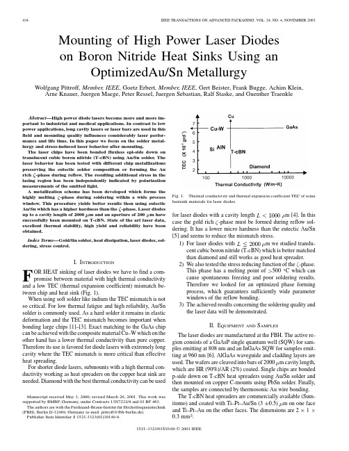
434IEEE TRANSACTIONS ON ADV ANCED PACKAGING,VOL.24,NO.4,NOVEMBER 2001Mounting of High Power Laser Diodes on Boron Nitride Heat Sinks Using anOptimizedAu/Sn MetallurgyWolfgang Pittroff ,Member,IEEE ,Goetz Erbert ,Member,IEEE ,Gert Beister,Frank Bugge,Achim Klein,Arne Knauer,Juergen Maege,Peter Ressel,Juergen Sebastian,Ralf Staske,and Guenther TraenkleAbstract—High power diode lasers become more and more im-portant to industrial and medical applications.In contrast to low power applications,long cavity lasers or laser bars are used in this field and mounting quality influences considerably laser perfor-mance and life time.In this paper we focus on the solder metal-lurgy and stress-induced laser behavior after mounting.The laser chips have been bonded fluxless epi-side down on translucent cubic boron nitride (T-cBN)using Au/Sn solder.The laser behavior has been tested with different chip metallizations preserving the eutectic solder composition or forming the Aurich-phase during soldering within a wide processwindow.This procedure yields better results then using eutectic Au/Sn which has a higher hardness thanthem and an aperture of200PublPITTROFF et al.:MOUNTING OF HIGH POWER LASER DIODES435Fig.2.Metal layer structures for Au/Sn die bonding:Ti—adhesion layer,Pt—diffusion barrier,thin Au—wetting layer (a)Eutectic Au/Sn composition preserves.(b) -phase forms,additional Au on the substrate.(c) -phase forms,additional Au on the chip.Chips are mounted using an eutectic die-bonder (Weld-Equip).We used a pulse heated thermode,controlled by an Unitek Phasemaster.Fluxless bonding is performed in anopen flow of forming gas N(10)heated up to 300-phase formation during reflow an additional Au layerhas to be introduced [7].It can be placed at the substrate side [Fig.2(b)]as proposed in [4].If using a thermode for reflow soldering this layer sequence has a serious disadvantage which is related to the heat flow from the thermode upwards to the die:First the Au/Sn solder will melt,the Au will start to dissolve andthe-phase arrives one will get a poor solder joint.This is strongly dependent onthe-phase will start growing onlyafter the chip surface has reached the soldering temperature.The soldering is not sensitive anymore tothe-phase.Applying the Au layer on the chip side[Fig.2(c)]we achieved highly reproducible bonds.Poor wetting which results in voids can cause localized stress [8]and localized heating near the active layer.As a first test of successful bonding we sheared off the chip at 300C).The metallization completely remains onthe heat spreader which proves the existenceofC.Thechip metallization has remained on the heat spreader except for two regions of poorwetting.-phase.No grain structure can be found.(The poor surfacequality of the polished cross section in the lower part of the solder layer is caused by the hardness difference between BN and solder alloy.)The dimensions and the soldering parameters of this attach-ment are listed as follows:Die Material:GaAs.Die metallization Ti–Pt–Au–Au plated.Substrate material:T-cBN.Substrate metallization:Ti–Pt–Au/Sn.Die dimensions:20001201000mC.For eutectic Au/Sn attachment [according to Fig.2(a)]wealso used the die metallization of Fig.2(c)and added another Pt–Au/200–100(nm)layer sequence on the chip.Thus only the last 100nm Au wetting layer will be dissolved in the Au/Sn solder.This differs slightly from the scheme of Fig.2(a):in addition there is the3100m)from the same wafer have been mounted both p-side up on copper C-mounts using Pb/Sn solder and p-side down on T-cBN using Au/Sn solder.P-side down mounting has been performed both using eutectic Au/Sn solder andusing436IEEE TRANSACTIONS ON ADV ANCED PACKAGING,VOL.24,NO.4,NOVEMBER2001Fig.4.SEM cross section of Au/Sn solder joint:(a)under the chip,where excess gold causes -phase growth.(b)Unmetallized area under the chip and beside the chip,where the eutectic preserves duringsoldering.Fig.5.Power-current characteristics of diode lasers coming from the same wafer and mounted in different ways.already at low optical output power which is probably caused by unwanted ring lasing modes appearing in addition to the Fabry–Perot modes.These ring modes cannot be observed di-rectly at p-side down mounted diode lasers but they have been studied at different structures showing ring modes even at p-side up mounted laser chips.In this case the scattered light of ring modes leaving the top face of the chip can be observed (Fig.6).The power-current characteristics show the same “power satu-ration”effect as seen in Fig.5.This lasing behavior seems to be affected by the interaction of the built-in stress of the heterojunctions with the mismatch stress caused by mounting.We can proof that by the following experiment.Mismatch stress begins at the solidifying point of the solder and increases during cooling down.Thus,upon in-creasing the heat sink temperature of the soldered laser diode the mismatch stress again decreases.This can indeed be demon-strated with the eutectically mounted samples shown in Fig.5:With increasing heat sink temperature the undisturbed laser ac-tion can be extended to higher optical output levels although the laser efficiency decreases (Fig.7).In the last case,if mounting p-side downwithm and the aper-ture (stripewidthm and200-phaseattachment is used.One example of “insensitive“laser structures which can be mounted using the eutectic solder composition is shown in Fig.9.Characteristics of a laser diode emitting at 808nm at different temperatures are sers with excellent high temperature operation data can be produced if the chip structure has high heterobarriers for low leakage current to ensure high thermal stability [9].V .S TRESS M EASUREMENTThus one could conclude that the amount of mismatch stress due to mounting influences the laser behavior and that the value of stress increases depending on mounting technique in the fol-lowing order:1)p-side up (This is obvious);2)p-side downwithPITTROFF et al.:MOUNTING OF HIGH POWER LASER DIODES437Fig.6.Loop lasing modes can be observed at p-side up mounted laser chips by the scattered light leaving the top face.(a)View on to the top face.(b)The threeloop modes of(a)are highlighted by lines forming a closed figure.The view on to the top face is inverted in contrast for bettervisibility.Fig.7.Power-current characteristics of diode laser mounted p-side down on T-cBN with eutectic Au/Sn ser action improves with increasing temperature,which indicates mismatch stress between chip and heat spreader. However,direct measurements of the stress along the active stripeinof the spontaneous facet emission far below the threshold current which is mainly caused by the splitting of the heavy-and light-hole bands.This splitting depends on the size of the quantum well and on the ratio of tensile or compressive stressinandand are the stresses inthe:drivingcurrentandm which is enough to438IEEE TRANSACTIONS ON ADV ANCED PACKAGING,VOL.24,NO.4,NOVEMBER2001Fig.9.Power-current characteristics of a laser diodes at different heat sink temperatures.Heating up to 85m wide stripe.The results obtained for the samples shown in Figs.5and 7are demonstrated in Fig.11.The10K )on T-cBN (TEC4causes tensile stress within the chip,which reduces the built-in stress of the quantum well.This reduction is considerable if mounting the laser chips p-side down,resulting in reduced degree of polarization.Unexpectedly,contrary to our conclusion above,the highest mismatch stress corresponds tothe-phase attachmentcan easily be explained by the solidification temperature of330C (soldering temperature),which is much higher than the freezing temperature of the eutectic solder (280-phase.It may be connected to the different solidification mecha-nisms.The solidificationby-phase formationas standard technique for broad area laser diodes up to2000K/W @Wm100K/W@Wm(mounting p-side down on T-cBN and C-mount).With laser diodes emitting in the 950nm range andW m [12],we achieve 9W optical output limited by thermal roll over (Fig.12).Reliability tests of these diode lasers have been performed at constant optical power.The drivingcurrentwedefine a degradationratelower than1PITTROFF et al.:MOUNTING OF HIGH POWER LASER DIODES439Fig.12.Power–current characteristics of a diode laser mounted p-side down on T-cBN with Au/Sn solder using -phase ser action is limited by thermal rollover.Fig.13.Aging test with laser diodes emitting at 935nm over 2000h at 25C to 50C a t a n o p t i c a l o u t p u t p o w e r o f 1.5W.T h e e x a m p l e o f f i v e l a s e r d i o d e s e m i t t i n g a t 950n m (c o m p r e s s i v e l y s t r a i n e d q u a n t u m w e l l ,A l -f r e e )i s s h o w n i n F i g .15.T h r e e d i o d e s h a d s u r v i v e d w h e n t h e t e s t w a s s w i t c h e d o f f a f t e r 3000h .V I I .C O N C L U S I O N S F l u x l e s s a n d p r e -f o r m f r e e m o u n t i n g o f l a s e r d i o d e s u s i n g A u /S n s o l d e r h a s b e e n p e r f o r m e d .B o r o n n i t r i d e h a s b e e n u s e da s h e a t s p r e a d e rb e t w e e nc h i p a nd c o p pe r s u b m o u n t .F o r m a t i o n of t h eg o l d r i c hCa t s ub s e q u e n t o p t ic a l p o w e r 1.5W ,2.0W ,a nd 2.5W f o r s t r i p =100 m.F i g .15.A g i n g t e s t w i t h l a s e r d i o d e s e m i t t i n g a t 950n m o v a t s u b s e q u e n t h e a t s i n k t e m p e r a t u r e 25C ,a n d 70-p h a s e f r e e z e s i m m e d i a t e l y d u e t om e l t i ng t e m p e r a t u r e .P -s i d e d o w n m o u n t i n g o f 2d i o d e s o n T -c B N h s b e e n p e r f o r m e d w i t h h i g h r E x c e l l n t t h e r m a l s t a b i l i t y o f m o u n t e d l a s e r d a c h i e ve d :O n l y 15%d r o p i n o p t i c a l o u t p u tf r o m h a s b e e n r e c o r d e d a s h e a t s i n k t e m p e r a t u r e r i s eC .D e g r a d a t i o n t e s t s w i t h o u t p u t p o w e r u p t o 2.5Wt e m p e r a t u r e u p t o 70440IEEE TRANSACTIONS ON ADV ANCED PACKAGING,VOL.24,NO.4,NOVEMBER2001R EFERENCES[1] C.C.Lee,C.Y.Wang,and G.S.Matijasevic,“A new bonding tech-nology using gold and tin multilayer composite structures,”IEEE Trans.Comp.,Hybrids,Manufact.Technol.,vol.14,pp.407–412,June1991.[2]G.S.Matijasevic and C.C.Lee,“V oid-free Au–Sn eutectic bonding ofGaAs dice and its characterization using scanning acoustic microscopy,”J.Electron.Mater.,vol.18,pp.327–337,1989.[3]G.S.Matijasevic,C.Y.Wang,and C.C.Lee,“V oid free bonding oflarge silicon dice using gold–tin alloys,”IEEE p.,Hybrids,Manufact.Technol.,vol.13,pp.1128–1134,1990.[4]S.Weiss,E.Zakel,and H.Reichl,“Mounting of high power laserdiodes on diamond heat sinks,”IEEE p.,Packag.,Manufact.Technol.A,vol.19,pp.46–53,Mar.1996.[5] C.Kallmayer,H.Oppermann,J.Kloeser,E.Zakel,and H.Reichl,“Ex-perimental results on the self-alignment process using Au/Sn metallurgyand on the growth of the -phase during the reflow,”in Proc.7th ITAP,San Jose,CA,1995,pp.225–238.[6]G.Erbert,G.Beister,F.Bugge,A.Knauer,R.Hülsewede,W.Pittroff,J.Sebastian,H.Wenzel,M.Weyers,and G.Trankle,“Performance of3W/100 m stripe diode lasers at950and810nm,”Proc.SPIE,vol.4287,2001.[7]T.B.Massalski,Binary Alloy Phase Diagrams,2nd ed.Metals Park,OH:ASM,1992,vol.3,p.2863.[8]R.K.Shukla and N.P.Mencinger,“A critical review of VLSI die at-tachment in high reliability application,”Solid State Technol.,vol.28,pp.67–74,1985.[9]W.Pittroff,F.Bugge,G.Erbert,A.Knauer,J.Maege,J.Sebastian,R.Staske,A.Thies,H.Wenzel,and G.Traenkle,“Highly reliable tensilystrained810nm QW laserdiode operating at high temperatures,”in Proc.LEOS’98,Orlando,FL,1998,pp.278–279.[10]P.D.Colbourne and D.T.Cassidy,“Imaging of stresses in GaAsdiode lasers using polarization-resolved photoluminescence,”IEEE J.Quantum Electron.,vol.29,pp.62–68,Jan.1993.[11] A.A.Ptashchenko,M.V.Deych,N.B.Mironchenko,and F.A.Ptashchenko,“Polarization of the spontaneous radiation of stressedlaser heterostructures,”Solid State Electron.,vol.37,pp.1255–1258,1994.[12]G.Erbert,G.Beister,A.Knauer,J.Maege,W.Pittroff,P.Ressel,J.Se-bastian,R.Staske,H.Wenzel,M.Weyers,and G.Tränkle,“Al-free950nm BA lasers with high efficiency and reliability at50PITTROFF et al.:MOUNTING OF HIGH POWER LASER DIODES441Peter Ressel received the M.S.degree in physics from the Friedrich-Schiller University,Jena,Ger-many and the Ph.D.degree in electrical engineering from the Technical University of Darmstadt, Germany,in1998.From1987to1991,he was working in the field of semiconductor lasers in the Academy of Sciences, GDR.In1992,he joined the Ferdinand Braun Insti-tute,Berlin,Germany,where his work concentrated on Ohmic contacts to InGaAs.Now his interests are focused on optical coatings for semiconductor lasers.Dr.Ressel is member of the Materials ResearchSociety.Juergen Sebastian was born in Dresden,Germany,in1958.He received the M.S.degree in physics fromthe Friedrich-Schiller-University,Jena,Germany,in1985and the Ph.D.degree in physics from HumboldtUniversity,Berlin,Germany,in1992.From1985to2001,he has been working in thefield of semiconductor laser technology and physics.In1986and1987,he was a Guest Scientist at the J.I.Alferov Laboratory,“Joffe-Institute,”St.Petersburg,Russia,engaged in the development and investigationof DFB-Laser for1.55 m.He is currently employed as a permanent staff member in the Optoelectronics Department,Ferdinand-Braun-Institute,Berlin,Germany,and responsible for the technology of high power semiconductor laserdiodes.Ralf Staske received the M.S.degree in physics formHumboldt University,Berlin,Germany.From1979to1989,he was dealing with pho-toluminescence investigations of semiconductormaterials.From1990to1997,he was working in thefield of sub- m movement and position detection forlaser-fiber-coupling.Since1997,his main tasks areinvestigations of optical,electrooptical,and thermalproperties of semiconductor laserdiodes.Guenther Traenkle received the M.S.degree inphysics from the Technical University of Munich(TU Munich),Germany,in1981and the Ph.D.degree in physics from the University of Stuttgart,Germany,in1988.At the University of Stuttgart,he worked onquantization and many-bode effects in III/Vquantum well structures.In1988,he joined theWalter-Schottky-Institute,TU Munich,running itsIII/V-semiconductor technology and working onfield-effect transistors and laser diodes.From1995 to1996,he was a Department Head at the Fraunhofer-Institute for Applied Solid-State Physics,Freiburg,Germany,and was responsible for the devel-opment and realization of electronic and optoelectronic III–V semiconductor devices,as well as quantum well infrared detector arrays.In August1996,he became head of the Ferdinand-Braun-Institute,Berlin.Since1999,he has also become Chairman of the Forschungsverbund Berlin e.V.His current research interests include GaAs technology,micro-wave and millimeter-wave transistors and circuits,GaN electronics,and high power diode lasers.。
FLGA中文资料

FEATURES•Low profile•Flexible body sizes range from 4 x 4mm to 13 x 13mm •Flip chip and discrete passive options (SiP)•Minimum 0.50mm pitch (array and peripheral land pads)•Flexible land pattern arrangement•Pb-free and halogen-free compatible materials available •JEDEC standard compliantAPPLICATIONS•Handheld devices •Wireless RF •Analog •ASIC •Memory •Simple PLDsDESCRIPTIONSTATS ChipPAC’s FLGA is a laminate substrate based package with plastic overmolded encapsulation. Unlike a standard FBGA, second level interconnect is achieved on the LGA by connecting “lands” on the package directly onto the PCB through solder re-flow. The elimination of solder balls brings better electrical performance and lower package profile without using the more expensive thinner BT core material.It also offers the flexibility of land pattern arrangement in the form of signal lands or heat spreader/ground pads to suit the thermal and electrical requirements of various devices. The FLGA package’s reduced outline and thickness make it an ideal advanced technology packaging solution for high performance and/or portable applications. STATS ChipPAC’s FLGA is available in a broad range of JEDEC standard body sizes including TFLGA (<1.20mm), VFLGA (<1.00mm) and WFLGA (<0.80mm) package thickness.FLGAFine Pitch Land Grid ArrayThe STATS ChipPAC logo is a registered trademark of STATS ChipPAC Ltd. All other product names and other company names herein are for identification purposes only and may be the trademarks or registered trademarks of their respective owners. STATS ChipPAC disclaims any and all rights in those marks. STATS ChipPAC makes no guarantee or warranty of its accuracy in the information given, or that the use of such information will not infringe on intellectual rights of third parties. Under no circumstances shall STATS ChipPAC be liable for any damages whatsoever arising out of the use of, or inability to use the materials in this document.STATS ChipPAC reserves the right to change the information at any time and without notice.©Copyright 2006. STATS ChipPAC Ltd. All rights reserved.May 2006Corporate Office 10 Ang Mo Kio St. 65, #05-17/20 Techpoint, Singapore 569059 Tel: 65-6824-7777 Fax: 65-6720-7823Global Offices USA 510-979-8000 JAPAN 81-3-5789-5850 CHINA 86-21-5976-5858 MALAYSIA 603-4257-6222 KOREA 82-31-639-8911 TAIWAN 886-3-593-6565 UK 44-1483-413-700 NETHERLANDS 31-38-333-2023FLGAFine Pitch Land Grid ArraySPECIFICATIONSDie Thickness75–300µm (3-12 mils)Mold Cap Thickness 0.25-0.90mm MarkingLaserPacking OptionsTape & reel/JEDEC trayRELIABILITYMoisture Sensitivity Level JEDEC Level 2A, 260°C Reflow Temperature Cycling Condition C (–65°C to 150°C),1000 cycles High Temp Storage 150°C, 1000 hrsPressure Cooker Test121°C/100%RH/2atm, 168 hrs Temperature/Humidity Test 85°C/85% RH, 1000 hrsUnbiased HAST130°C/85% RH/2 atm, 96 hrsCROSS-SECTIONPACKAGE CONFIGURATIONSBody Sizes (mm) 4x4 to 13x13Terminal Count 8 to 200Terminal Pitch (mm) 0.50 to 0.80Typ. Pkg. Thickness TFLGA: 1.20mmVFLGA: 1.00mm max. WFLGA: 0.80mm max.ELECTRICAL PERFORMANCEElectrical parasitic data is highly dependent on the package layout. 3D electrical simulation can be used on the specific package design to provide the best prediction of electrical behavior. First order approximations can be calculated using parasitics per unit length for the constituents of the signal path. Data below is for a frequency of 100MHz and assumes 1.0 mil gold bonding wire.Conductor Length Resistance Inductance Inductance CapacitanceCapacitance Component (mm) (mOhms)(nH)Mutual (nH)(pF)Mutual (pF)Note: Net = Total Trace Length + ViaFLGATHERMAL PERFORMANCE,θja (°C/W)Thermal performance is highly dependent on package size, die size, substrate layers and thickness, and land configuration.Simulation for specific applications should be performed to obtain maximum accuracy.Package Body Size (mm)Pin Count Die Size PCB Vias Thermal Performance θja(ºC/W)Note: Simulation data for package mounted on 4 layer PCB (per JEDEC JESD51-9) under natural convection as defined in JESD51-2.。
AE94.3A燃气涡轮机说明书

THE GAS TURBINE: AE94.3AProven technology for efficient power generationFast, flexible and cost effectiveThe simple and robust design of the AE94.3A has made it possible toaccommodate continuous upgrades over the years, progressively enhancing performance while maintaining and even improving the level of reliability (> 99.5%). Its balanced thermal distribution throughout the entire enginecombined with its extreme operating simplicity enables high cycling capability. It can be started and stopped without any time limitation and reach base load in approx. 20 minutes, a key factor for grid stability and peak plants.Single shaft, internally air-cooled rotor , disk type with Hirth serration and central tierod 15 stages axial compressor with variable guide vanes*Annular type Combustion Chamber lined with individually replaceable tilesCold-end generator24 dry low NOx burners for premixoperation both for gas and for oil modeRotorDisplacementSystem (RDS) for gap optimization2 units fed with hydrogen enriched off gas inCommercial Operationsince 2006, with more than 250.000 EOH.4 stages, air cooled turbine, axial discharge, advanced cooling technique*Multi fuel and Hydrogen capableA wide selection of fuels can beused, ranging from natural gas with hydrocarbons in several proportion or with hydrogen content up to 40% vol, up to liquid fuels such as Diesel Oil, High Speed Diesel and Naphtha.*All vanes and blades replaceable with rotor in place.Via N. Lorenzi, 8 - 16152 Genoa - Italy Tel: +39 010 6551***********************Environmental sustainableNOx level down to 15 ppm in dry gas mode and 60 ppm in dry oil mode (with possibility to reach 25 ppm with small water amount .Smart maintenance approachCustomized service agreements, including upgrading packages, allow Customers to choose the best solution to fit their needs.• Extended time between majoroverhauls (up to 5 years, depending on operating conditions)• High durability of hot gas path parts •Quick on-site activitiesGeneral note: Performance data are calculated with 100% methane (LHV) at ISO conditions, direct cooling.495992CC Net Output (MW)6060.3CC Net Efficiency (%)5,9955,970CC Net Heat Rate (kJ/kWh)4525Plant Turndown Minimum load (%)40.3Efficiency (%)755Exhaust Mass Flow (Kg/s)593Exhaust Temperature (°C)40GT minimum load (%)340Power output (MW)total > 4 millions EOHReferences:Ansaldo Energia, all rights reserved. Trademarks mentioned in this document are the property of Ansaldo Energia, its affiliates, or their respective owners in the scope of registration. The information contained in this document is merely indicative. No representation or warranty is provided, nor should be relied on, that such information is complete or correct or will apply to any particular project. This will depend on the technical and commercial circumstances. Said information is provided without liability and is subject to change without notice. Reproduction, use or disclosure to third parties, without express written authority, is strictly prohibited.。
国家电子NI 9227 四通道、五臂、24位、同时、渠道间隔离模拟输入模块操作指南和规格说明书

Caution Ensure that hazardous voltage wiring is performed only by qualified personnel adhering to local electrical standards. Caution Do not mix hazardous voltage circuits and human-accessible circuits on the same module. Caution Make sure that devices and circuits connected to the module are properly insulated from human contact.
Services /services
2 | | NI 9227 Operating Instructions and Specifications
Safety Guidelines
Operate the NI 9227 only as described in these operating instructions.
Figure 5. Input Circuitry for One Channel of the NI 9227
AI+C
Amplifier Prefilter
NI 9227
NI 9227 Operating Instructions and Specifications | © National Instruments | 9
Related Information