IRL3803S_datasheet
艾茨顿199034产品说明说明书

Eaton 199034Eaton Moeller® series Rapid Link - Speed controllers, 8.5 A, 4 kW, Sensor input 4, Actuator output 2, 230/277 V AC, PROFINET, HAN Q4/2, with braking resistance, with fanGeneral specificationsEaton Moeller® series Rapid Link Speed controller199034195 mm270 mm 220 mm 3.65 kgUL 61800-5-1 IEC/EN 61800-5-1 UL approval RoHS CERASP5-8422PNT-4120101S1Product NameCatalog NumberProduct Length/Depth Product Height Product Width Product Weight Certifications Catalog Notes Model Code3 fixed speeds and 1 potentiometer speedcan be switched over from U/f to (vector) speed control Connection of supply voltage via adapter cable on round or flexible busbar junction480 VIs the panel builder's responsibility. The specifications for the switchgear must be observed.400 V AC, 3-phase480 V AC, 3-phaseMeets the product standard's requirements.4 kW500 VMeets the product standard's requirements.-40 °C380 VThermo-click with safe isolationBraking resistance2 Actuator outputsIGBT inverterKey switch position AUTOPC connectionKey switch position HANDSelector switch (Positions: REV - OFF - FWD)FanKey switch position OFF/RESETPTC thermistor monitoringControl unitInternal DC linkBreaking resistanceTwo sensor inputs through M12 sockets (max. 150 mA) for quick stop and interlocked manual operation0 Hz Generation change from RA-SP to RASP 4.0Generation change RAMO4 to RAMO5Generation change from RA-MO to RAMO 4.0Configuration to Rockwell PLC for Rapid LinkGeneration Change RA-SP to RASP5Generation Change RASP4 to RASP5Rapid Link 5 - brochureDA-SW-USB Driver DX-COM-STICK3-KITDA-SW-USB Driver PC Cable DX-CBL-PC-1M5DA-SW-Driver DX-CBL-PC-3M0DA-SW-drivesConnect - installation helpDA-SW-drivesConnect - InstallationshilfeDA-SW-drivesConnectMaterial handling applications - airports, warehouses and intra-logistics ETN.RASP5-8422PNT-4120101S1.edzIL034093ZUramo5_v36.dwgrasp5_v36.stpDA-DC-00003964.pdfDA-DC-00004184.pdfDA-DC-00004514.pdfDA-DC-00004508.pdfeaton-bus-adapter-rapidlink-speed-controller-dimensions-002.eps eaton-bus-adapter-rapidlink-speed-controller-dimensions-003.eps eaton-bus-adapter-rapidlink-speed-controller-dimensions.epseaton-bus-adapter-rapidlink-speed-controller-dimensions-004.epsMains voltage - max10.11 Short-circuit ratingRated operational voltage10.4 Clearances and creepage distancesOutput at quadratic load at rated output voltage - max Output voltage - max10.2.3.1 Verification of thermal stability of enclosures Ambient storage temperature - minMains voltage - minFitted with:Output frequency - min Applikasjonsmerknader BrosjyrereCAD model Installeringsinstruksjoner mCAD model SertifiseringsrapporterTegningerStarting current - max200 %, IH, max. starting current (High Overload), For 2 seconds every 20 seconds, Power sectionRated conditional short-circuit current (Iq)10 kAAmbient operating temperature - max40 °CCommunication interfacePROFINET, optionalAssigned motor power at 115/120 V, 60 Hz, 1-phase5 HPOutput frequency - max500 HzSwitching frequency8 kHz, 4 - 32 kHz adjustable, fPWM, Power section, Main circuitFeaturesParameterization: drivesConnect mobile (App) Parameterization: FieldbusInternal and on heat sink, temperature-controlled Fan Parameterization: drivesConnectParameterization: KeypadAmbient operating temperature - min-10 °CBraking current≤ 0.6 A (max. 6 A for 120 ms), Actuator for external motor brakeNumber of HW-interfaces (serial TTY)10.6 Incorporation of switching devices and componentsDoes not apply, since the entire switchgear needs to be evaluated.Nominal output current I2N8.5 A10.2.6 Mechanical impactDoes not apply, since the entire switchgear needs to be evaluated.10.3 Degree of protection of assembliesDoes not apply, since the entire switchgear needs to be evaluated.Product categorySpeed controllerRadio interference classC2, C3: depending on the motor cable length, the connected load, and ambient conditions. External radio interference suppression filters (optional) may be necessary.C1: for conducted emissions onlyHeat dissipation capacity Pdiss0 WRated control voltage (Uc)230/277 V AC (external brake 50/60 Hz)24 V DC (-15 %/+20 %, external via AS-Interface® plug)Assigned motor power at 460/480 V, 60 Hz, 3-phase5 HPNumber of HW-interfaces (RS-422)Mains current distortion120 %ProtocolPROFINET IO10.9.2 Power-frequency electric strengthIs the panel builder's responsibility.Overvoltage categoryIIIDegree of protectionIP65NEMA 12Ambient storage temperature - max70 °CRated impulse withstand voltage (Uimp)2000 VConnectionPlug type: HAN Q4/2Overload currentFor 60 s every 600 sAt 40 °CFunctionsFor actuation of motors with mechanical brake3 fixed speeds1 potentiometer speedBrake chopper with braking resistance for dynamic braking4-quadrant operation possibleOutput at linear load at rated output voltage - max4 kWMains voltage tolerance380 - 480 V (-10 %/+10 %, at 50/60 Hz)Leakage current at ground IPE - max3.5 mAConverter typeU converter10.2.2 Corrosion resistanceMeets the product standard's requirements.Supply frequency50/60 Hz10.2.4 Resistance to ultra-violet (UV) radiationMeets the product standard's requirements.10.2.7 InscriptionsMeets the product standard's requirements.Shock resistance15 g, Mechanical, According to IEC/EN 60068-2-27, 11 ms, Half-sinusoidal shock 11 ms, 1000 shocks per shaftApplication in domestic and commercial area permittedYesNumber of inputs (analog)Number of phases (output)310.12 Electromagnetic compatibilityIs the panel builder's responsibility. The specifications for the switchgear must be observed.10.2.5 LiftingDoes not apply, since the entire switchgear needs to be evaluated.Number of HW-interfaces (RS-485)1Number of HW-interfaces (industrial ethernet)Efficiency98 % (η)System configuration typePhase-earthed AC supply systems are not permitted.AC voltageCenter-point earthed star network (TN-S network)10.8 Connections for external conductorsIs the panel builder's responsibility.Switch-on threshold for the braking transistor765 VDCProtectionFinger and back-of-hand proof, Protection against direct contact (BGV A3, VBG4)Braking voltage230/277 V AC -15 % / +10 %, Actuator for external motor brakeApplication in industrial area permittedYesClimatic proofingIn accordance with IEC/EN 50178< 95 %, no condensation10.9.3 Impulse withstand voltageIs the panel builder's responsibility.Overload current IL at 150% overload12.7 AInput current ILN at 150% overload7.8 ANumber of HW-interfaces (RS-232)Number of inputs (digital)4Current limitationAdjustable, motor, main circuit0.8 - 8.5 A, motor, main circuitCable lengthC3 ≤ 25 m, maximum motor cable lengthC1 ≤ 1 m, maximum motor cable lengthC2 ≤ 5 m, maximum motor cable length10.5 Protection against electric shockDoes not apply, since the entire switchgear needs to beevaluated.Mounting positionVerticalMains switch-on frequencyMaximum of one time every 60 seconds10.13 Mechanical functionThe device meets the requirements, provided the information in the instruction leaflet (IL) is observed.10.9.4 Testing of enclosures made of insulating materialIs the panel builder's responsibility.Heat dissipation per pole, current-dependent Pvid0 WElectromagnetic compatibility1st and 2nd environments (according to EN 61800-3)Resolution0.1 Hz (Frequency resolution, setpoint value)Assigned motor power at 460/480 V, 60 Hz5 HPRelative symmetric net voltage tolerance10 %Rated operational current (Ie)8.5 A at 150% overload (at an operating frequency of 8 kHz and an ambient air temperature of +40 °C)Number of outputs (analog)Rated operational power at 380/400 V, 50 Hz, 3-phase4 kWNumber of HW-interfaces (USB)Operating modeSensorless vector control (SLV)PM and LSPM motorsSynchronous reluctance motorsBLDC motorsU/f controlRated frequency - min45 HzDelay time< 10 ms, On-delay< 10 ms, Off-delayNumber of outputs (digital)2Power consumption95 W10.2.3.2 Verification of resistance of insulating materials to normal heatMeets the product standard's requirements.10.2.3.3 Resist. of insul. mat. to abnormal heat/fire by internal elect. effectsMeets the product standard's requirements.Number of HW-interfaces (other)Rated frequency - max66 HzVibrationResistance: According to IEC/EN 60068-2-6Resistance: 6 Hz, Amplitude 0.15 mmResistance: 10 - 150 Hz, Oscillation frequency Resistance: 57 Hz, Amplitude transition frequency on accelerationShort-circuit protection (external output circuits)Type 1 coordination via the power bus' feeder unit, Main circuit10.7 Internal electrical circuits and connectionsIs the panel builder's responsibility.Braking torque≤ 30 % (I/Ie)Adjustable to 100 % (I/Ie), DC - Main circuitRelative symmetric net frequency tolerance10 %10.10 Temperature riseThe panel builder is responsible for the temperature rise calculation. Eaton will provide heat dissipation data for the devices.Number of HW-interfaces (parallel)Assigned motor power at 230/240 V, 60 Hz, 1-phase5 HPInterfacesNumber of slave addresses: 31 (AS-Interface®)Eaton Corporation plc Eaton House30 Pembroke Road Dublin 4, Ireland © 2023 Eaton. Med enerett.Eaton is a registered trademark.All other trademarks are property of their respectiveowners./socialmediaMax. total power consumption from AS-Interface® power supply unit (30 V): 250 mASpecification: S-7.4 (AS-Interface®)351.6 W at 25% current and 0% speed 53.8 W at 25% current and 50% speed 60.9 W at 50% current and 0% speed 64 W at 50% current and 90% speed 65.4 W at 50% current and 50% speed 85.1 W at 100% current and 0% speed 94 W at 100% current and 50% speed 95.3 W at 100% current and 90% speed 2Max. 2000 mAbove 1000 m with 1 % performance reduction per 100 mNumber of phases (input)Heat dissipation at current/speed Number of interfaces (PROFINET)Altitude。
AO4803A;中文规格书,Datasheet资料

THIS PRODUCT HAS BEEN DESIGNED AND QUALIFIED FOR THE CONSUMER MARKET. APPLICATIONS OR USES AS CRITICAL COMPONENTS IN LIFE SUPPORT DEVICES OR SYSTEMS ARE NOT AUTHORIZED. AOS DOES NOT ASSUME ANY LIABILITY ARISING OUT OF SUCH APPLICATIONS OR USES OF ITS PRODUCTS. AOS RESERVES THE RIGHT TO IMPROVE PRODUCT DESIGN, FUNCTIONS AND RELIABILITY WITHOUT NOTICE.
Gate-Source Voltage
VGS
Continuous Drain
TA=25°C
Current
TA=70°C
Pulsed Drain Current C
Avalanche Current C
Avalanche energy L=0.1mH C
ID
IDM IAS, IAR EAS, EAR
TA=25°C Power Dissipation B TA=70°C
PD
Junction and Storage Temperature Range
TJ, TSTG
Maximum -30 ±20 -5 -4 -30 17 14 2 1.3
datasheet-pam2803

FeaturesLED Power Efficiency:up to 90%Current Accuracy:5%(V =3.6V to 1.8V@V =3.7V)1MHz Switching FrequencyUses small,Low Profile External Components Low RDS(ON):100mΩ(TYP.)Open LED ProtectionOver Temperature Protection Low Profile SOT-23-6Package Pb-Free Package±IN F Low Start-Up Voltage:0.9V(I =270mA)Low Hold Voltage:0.75V(I =200mA)White LED Torch (Flashlight)White LED Camera FlashDSC(Digital Still Camera)Flash Cellular Camera Phone Flash PDA Camera FlashCamcorder Torch(Flashlight)LampThe PAM2803is a set-up DC-DC converter that delivers a regulated output current.The device switches at a 1.0MHz constant frequency,allowing for the use of small value external inductor and ceramic capacitors.The PAM2803is targeted to be used for driving loads up to 1A from a two-cell alkaline battery.The LED current can be programmed by the external current sense resistor,Rs,connected between the feedback pin (FB)and ground.A low 95mV feedback voltage reduces the power loss in the Rs for better efficiency.With its internal 2A,100device can provide high efficiency even at heavy load.During the shutdown mode,the feedback resistor Rs and the load are completely disconnected and the current consumption is reduced to less than 1uA.The PAM2803is available in the 6-lead SOT-23-6package.LED LED ApplicationsGeneral Descriptio nmΩNMOS switch,the n n n n n n n n n n n n n n n n nTypical ApplicationBlock DiagramC OLED SPin Configuration&Marking InformationTop View SOT 236--123654Pin NumberName Function 1SW Switch 2GND Ground 3FB Feedback 4SHDN Shut Down 5VOUT Output 6VINInputAbsolute Maximum RatingsThese are stress ratings only and functional operation is not implied Exposure to absolute maximum ratings for prolonged time periods may affect device reliability All voltages are with respect to ground ...Input Pin Voltage ...............................–0.3V to 6V SW Pin Voltage..................................–0.3V to 6V SHDN,FB Pin Voltage.........................–0.3V to 6VOperating Temperature Range .........-40C to 85C Storage Temperature Range.........–65C to 125C Lead Temperature (Soldering,5sec)...........300C°°°°°Recommended Operating ConditionsJunction Temperature 40to 125-...............C C..................C C°°°°Ambient Temperature 40to 85-Thermal InformationXX:Product Code V:Voltage Code Y:Year W:WeeklyElectrical CharacteristicT =25,V =2.4V,I =750mA,V =V ,L=2.2uH,C =10uF,C =10uF,unless otherwise noted.A IN LED SHDN IN ΙΝO ℃Note1:V -LED Forward VoltageF ParameterSymbol ConditionsMin TypMax Unit Input Voltage Range V IN 0.9VF-0.2(note 1)V Feedback Voltage V FB 9095100mV Start-up Voltage V START V IN :0V →3V I LED =270mA 0.9V Hold Voltage V HOLD V IN :3V →0V I LED :750mA →200mA0.75V Oscillator Frequency F OSC 0.85 1.01.15MHz SHDN Input High V SH V IN =1.8V 1.0V SHDN Input LowV SL V IN =1.8V0.4V Over Temperature Shutdown OTS 150℃Over Temperature Hysteresis OTH 15℃Maximum Output Current RangeI O(MAX)750mA Quiescent Current I Q I LED =0mA,V O =3.4V,Device Switching at 1MHz 13mA Shutdown Current I SD Shutdown mode 1uA Switch on Resistance R DSON V O =3.4V 0.1ΩCurrent Limit I LIM V O =3.4V 2A EfficiencyηI LED =750mA90%Typical Performance CharacteristicsT =25,L=2.2uH ,C =10uF,C =10uF,unless otherwise noted.A ΙΝΟ℃400450500550600650700750800Input Voltage(V)L E D C u r r e n t (m A )50556065707580859095100 1.21.51.82.12.42.733.33.6Input Voltage(V)F e e d b a c k V o l t a g e (m V )5007009001100130015001700190021002300 1.21.51.82.12.42.733.33.6Input Voltage(V)D C I n p u t C u r r e n t (m A )1.LED Power Efficiency vs Input Voltage2.LED Current vs Input Voltage4.Feedback Voltage vs Input Voltage (I =750mA@V =3.7V)LED F 4050607080901001.21.51.82.12.42.733.33.6Input Voltage(V)L E D P o w e r E f f i c i e n c y (%)Typical Performance Characteristics (continued )7.Overvoltage ProtectionSW V AC CouplingO IL5.Switching Waveform6.Start-Up WaveformSHDNI LV OInductor SelectionCapacitor SelectionDiode SelectionLED Current SettingThe PAM2803can use small value inductors due to its switching frequency of 1MHz.The value of inductor will focus in the range of 2.2uH to 4.7uH for most PAM2803applications.In typical high c u r r e n t w h i t e L E D a p p l i c a t i o n s ,i t i s recommended to use a 4.7uH inductor.The inductor should have low DCR (DC resistance)to minimize the I R power loss,and it requires a current rating of 2A to handle the peak inductor current without saturating.An input capacitor is required to reduce the input ripple and noise for proper operation of the PAM2803.For good input decoupling,Low ESR (equivalent series resistance)capacitors should be used at the input.At least 2.2uF input capacitor is recommended for most applications.A minimum output capacitor value of 6.8uF is r e c o m m e n d e d u n d e r n o r m a l o p e r a t i n g conditions,while a 10uF-22uF capacitor may be required for higher power LED current.A reasonable value of the output capacitor depends on the LED current.The ESR of the output capacitor is the important parameter to determine the output voltage ripple of the converter,so low ESR capacitors should be used at the output to reduce the output voltage ripple.The small size of ceramic capacitors is an excellent choice for PAM2803applications.The X5R and X7R types are preferred because they maintain capacitance over wide voltage and temperature ranges.It's indispensable to use a Schottky diode rated at 2A with the ing a Schottky diode with a lower forward voltage drop is better to improve the power LED efficiency,and its voltage rating should be greater than the output voltage.I n a p p l i c a t i o n ,t h e O N S e m i c o n d u c t o r MBRA210LT3G is recommended.The LED current is set by the single external Rs resistor connected to the FB pin as shown in the typical application circuit on page 1.The typical FB reference is internally regulated to 95mV.The LED current is 95mV/Rs.It's recommended to use a 1%or better precision resistor for the better LED current accuracy.The formula and table 1for Rs selection are shown as follows:Rs=95mV/I Table 1.Rs Resistor Value Selection 2LEDPCB Layout GuidelinesAs for all switching power supplies,the layout and components placement of the PAM2803is an important step in the design;especially at h i g h p e a k c u r r e n t s a n d h i g h s w i t c h i n g frequencies.The input capacitor and output capacitor should be placed respectively as close as possible to the input pin and output pin of the IC;the inductor and schottky diode should be placed as close as possible to the switch pin by using wide and short traces for the main current path;the current sense resistor should be placed as close as possible between the ground pin and feedback pin.Application InformationStandard Value(Ω)I LED (mA)0.185280.156330.127920.10950Ordering InformationPlease consult PAM sales office or authorized Rep Distributor for detailed ordering information../FB Voltageof Pins Type PAM2803Pin Configuration Package Type Number of PinsFB Voltage A Type1.SW2.GND3.FB4.SHDN5.VOUT6.VINA:SOT-23-6F:6095:95mVPart Number Marking Package Type Standard Package PAM2803AAF095CFAYWSOT-23-63,000Units/Tape&ReelOutline DimensionSOT 236--GAUGE PLANE SEATING PLANEBASESECTION A-ASEE VIEWSSymbol AA1A2b c D E Spec 1.20±0.250.10±0.05 1.10±0.20.40±0.10.15±0.0.7 2.90±0.12.80±0.2Symbol E11e e 1LL1θSpec1.60±0.10.95BSC1.90BSC 0.55±0.250.60REF4°±4°。
IR2103SPBF;IR2103PBF;IR2103STRPBF;IR2103;IR2103S;中文规格书,Datasheet资料
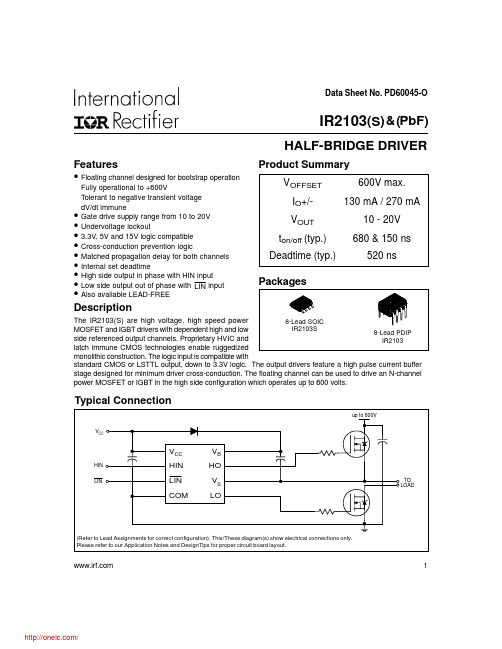
Data Sheet No. PD60045-OTypical ConnectionProduct SummaryHALF-BRIDGE DRIVERFeatures•Fully operational to +600VdV/dt immune••Undervoltage lockout••Cross-conduction prevention logic••Internal set deadtime•••Also available LEAD-FREEDescriptionpower MOSFET or IGBT in the high side configuration which operates up to 600 volts. 1IR2103(S ) & (PbF)IR2103(S) & (PbF)Absolute Maximum RatingsAbsolute maximum ratings indicate sustained limits beyond which damage to the device may occur. All voltage param-eters are absolute voltages referenced to COM. The thermal resistance and power dissipation ratings are measured under board mounted and still air conditions.Note 1: Logic operational for V S of -5 to +600V. Logic state held for V S of -5V to -V BS . (Please refer to the Design Tip DT97-3 for more details).IR2103(S) & (PbF) 3Static Electrical CharacteristicsV BIAS (V CC , V BS ) = 15V and T A = 25°C unless otherwise specified. The V IN , V TH and I IN parameters are referenced to COM. The V O and I O parameters are referenced to COM and are applicable to the respective output leads: HO or LO.Dynamic Electrical CharacteristicsV BIAS (V CC , V BS ) = 15V, C L = 1000 pF and T A = 25°C unless otherwise specified.IR2103(S) & (PbF)4Functional Block DiagramLead DefinitionsSymbol DescriptionHIN Logic input for high side gate driver output (HO), in phase Logic input for low side gate driver output (LO), out of phase VB High side floating supply HO High side gate drive output V S High side floating supply return V CC Low side and logic fixed supply LO Low side gate drive output COMLow side returnLINLead Assignments8 Lead PDIP 8 Lead SOICIR2103IR2103S12348765V CC HIN LIN COMV B HO V S LO12348765V CC HIN LIN COMV B HO V S LOIR2103(S) & (PbF) 5Figure 1. Input/Output Timing DiagramLINHOLOHINFigure 4. Deadtime Waveform DefinitionsFigure 2. Switching Time Waveform DefinitionsLOIR2103(S) & (PbF)6IR2103(S) & (PbF) 7IR2103(S) & (PbF)8IR2103(S) & (PbF)9IR2103(S) & (PbF)10vs Temperaturevs Voltage分销商库存信息:IRIR2103SPBF IR2103PBF IR2103STRPBF IR2103IR2103S IR2103STR。
IRL3103资料
ISD ≤ 34A, di/dt ≤ 120A/µs, VDD ≤ V(BR)DSS,
TJ ≤ 175°C
2
元器件交易网
IRL3103
1000
VGS 15V 10V 4.5V 3.7V 3.5V 3.3V 3.0V BOTTOM 2.7V TOP
元器件交易网
PD - 91337
IRL3103
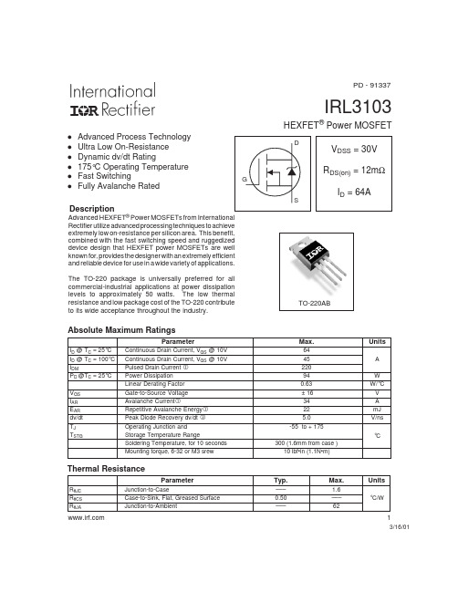
HEXFET® Power MOSFET
l l l l l l
Advanced Process Technology Ultra Low On-Resistance Dynamic dv/dt Rating 175°C Operating Temperature Fast Switching Fully Avalanche Rated
Min. Typ. Max. Units
Conditions D MOSFET symbol 64 ––– ––– showing the A G integral reverse ––– ––– 220 S p-n junction diode. ––– ––– 1.2 V TJ = 25°C, IS = 34A, VGS = 0V ––– 57 86 ns TJ = 25°C, IF = 34A ––– 110 170 nC di/dt = 100A/µs Intrinsic turn-on time is negligible (turn-on is dominated by LS+LD)
RDS(on) VGS(th) gfs IDSS IGSS Qg Qgs Qgd td(on) tr td(off) tf LD LS Ciss Coss Crss EAS
Min. 30 ––– ––– ––– 1.0 22 ––– ––– ––– ––– ––– ––– ––– ––– ––– ––– ––– ––– ––– ––– ––– ––– –––
TPS380XXXX(电源监控芯片)
TPS380x...DCK PACKAGE(TOP VIEW)RESETGNDMRV DDGNDTPS3801−01...DCK PACKAGE(TOP VIEW)RESETGNDSENSEV DDGNDTPS3800-xxTPS3801-xxTPS3802-xx SLVS219E–AUGUST1999–REVISED OCTOBER2010 ULTRA-SMALL SUPPLY VOLTAGE SUPERVISORSCheck for Samples:TPS3800-xx,TPS3801-xx,TPS3802-xxFEATURESDESCRIPTION•Small,5-Pin SC-70(SOT-323)Package•Supply Current of9m A The TPS380x family of supervisory circuits monitorsupply voltages to provide circuit initialization and •Power-On Reset Generator With Fixed Delaytiming supervision,primarily for DSPs and other Timeprocessor-based systems.–TPS3800=100msThese devices assert a push-pull RESET signal when –TPS3801=200msthe SENSE(adjustable version)or V DD(fixed version)–TPS3802=400ms drops below a preset threshold.The RESET outputremains asserted for the factory programmed delay •Precision Supply Voltage Monitor1.8V,2.5V,time after the SENSE or V DD return above its2.7V,3V,3.3V,5V,and Adjustablethreshold.•Manual Reset Input(Except TPS3801-01)The TPS380x devices,except the TPS3801-01,•Temperature Range:–40°C to+85°Cincorporate a manual reset input(MR).A low level atMR causes RESET to become active. APPLICATIONSThe TPS380x uses a precision reference to achieve •Applications Using DSPs,Microcontrollers,oran overall threshold accuracy of2%—2.5%.These Microprocessorsdevices are available in a5-pin SC-70package,•Wireless Communication Systemswhich is only about half the size of a5-pin SOT-23•Portable/Battery-Powered Equipment package.•Programmable ControlsThe TPS380x devices are fully specified over a •Intelligent Instrumentstemperature range of–40°C to+85°C.•Industrial Equipment•Notebook/Desktop Computers•Automotive SystemsPlease be aware that an important notice concerning availability,standard warranty,and use in critical applications of TexasInstruments semiconductor products and disclaimers thereto appears at the end of this data sheet.All trademarks are the property of their respective owners.PRODUCTION DATA information is current as of publication date.Copyright©1999–2010,Texas Instruments Incorporated Products conform to specifications per the terms of the TexasTPS3800-xxTPS3801-xxTPS3802-xxSLVS219E–AUGUST1999–REVISED These devices have limited built-in ESD protection.The leads should be shorted together or the device placed in conductive foam during storage or handling to prevent electrostatic damage to the MOS gates.AVAILABLE OPTIONS(1)T A DEVICE NAME THRESHOLD VOLTAGE TYP DELAY TIME MARKINGTPS3801-01DCK Adjustable(V ref=1.14V)200ms ARFTPS3801E18DCK 1.71V200ms ARETPS3801J25DCK 2.25V200ms NJATPS3800G27DCK 2.5V95ms ARITPS3801L30DCK 2.64V200ms NPA –40°C to85°CTPS3801K33DCK 2.93V200ms NWATPS3802L30DCK 2.64V380ms ASATPS3802K33DCK 2.93V380ms ARKTPS3801T50DCK 4.00V25ms AVITPS3801I50DCK 4.55V200ms NSA(1)For the most current package and ordering information,see the Package Option Addendum at the end of this data sheet,or refer to ourweb site at .ABSOLUTE MAXIMUM RATINGS(1)(2)Over operating free-air temperature range(unless otherwise noted).UNITSupply voltage,V DD7VSENSE–0.3V to5VAll other pins–0.3V to7VMR–0.3V to V DD+0.3VRESET–0.3V to V DD+0.3VMaximum low-output current,I OL5mAMaximum high-output current,I OH–5mAInput-clamp current,I IK(V I<0or V I>V DD)±20mAOutput-clamp current,I OK(V O<0or V O>V DD)±20mAOperating junction temperature range,T J(3)–40°C to+85°CStorage temperature range,T stg–65°C to+150°C(1)Stresses beyond those listed under absolute maximum ratings may cause permanent damage to the device.These are stress ratingsonly,and functional operation of the device at these or any other conditions beyond those indicated under recommended operating conditions is not implied.Exposure to absolute-maximum-rated conditions for extended periods may affect device reliability.(2)All voltage values are with respect to GND.For reliable operation,the device should not be operated at7V for more than t=1000hcontinuously.(3)Due to the low dissipation power of this device,it is assumed that T J=T A.RECOMMENDED OPERATING CONDITIONSMIN MAX UNIT TPS3801J25,TPS3801L30,TPS3801K33,TPS3801I50,TPS3801T5026Supply voltage,V DD VAll other devices 1.64SENSE0See(1)VInput voltage,V I0V DD+0.3VHigh-level input voltage,V IH0.7×V DD V DD+0.3VLow-level input voltage,V IL0.3×V DD VInput transition rise and fall rate at MR,Δt/ΔV100ns/VV Pull-upPull-up resistor value,RESETΩ50µAOperating free-air temperature range,T A–40+85°C(1)Maximum=V DD+0.3or4.5V,whichever is greater.2Submit Documentation Feedback Copyright©1999–2010,Texas Instruments IncorporatedTPS3800-xxTPS3801-xxTPS3802-xx SLVS219E–AUGUST1999–REVISED OCTOBER2010 ELECTRICAL CHARACTERISTICSOver–40°C to+85°C free-air temperature range(unless otherwise noted).TPS3800-xx,TPS3801-xx,TPS3802-xxPARAMETER TEST CONDITIONSMIN TYP MAX UNITV DD=1.6V to6V I OH=–500m A V DD–0.2V OH High-level output voltage(RESET)V DD=3.3V I OH=–2mA V DD–0.4VV DD=6V I OH=–4mA(1)V DD–0.4V DD=1.6V to6V,I OL=500m A0.2V OL Low-level output voltage(RESET)V DD=3.3V,I OL=2mA0.4VV DD=6V,I OL=4mA(1)0.4 Power-up reset voltage(2)V DD≥1.1V,I OL=50m A0.2VTPS380x-01 1.117 1.14 1.163TPS380xE18 1.67 1.71 1.75TPS380xJ25 2.2 2.25 2.3TPS380xG27 2.45 2.5 2.55 Negative-going inputV IT–T A=–40°C to85°C V threshold voltage(3)TPS380xL30 2.58 2.64 2.7TPS380xK33 2.87 2.93 2.99TPS380xI50 4.45 4.55 4.65TPS380xT50 3.924 4.08TPS380x-0115TPS380xx1825TPS380xx2530V hys Threshold hysteresis TPS380xx2735mVTPS380xx3035TPS380xx3340TPS380xx5060I IH High-level input current(MR)MR=0.7×V DD,V DD=6V–40–60–100m AI IL Low-level input current(MR)MR=0V,V DD=6V–130–200–340I I Input current(SENSE)–2525nATPS3801J25,V DD=2V,MR and output912TPS3801L30,unconnectedTPS3801K33,V DD=6V,MR and outputTPS3801I50,2025unconnectedTPS3801T50V DD=1.6V,SENSE=0V to V DD,710output unconnectedI DD Supply current m ATPS3801-01V DD=4V,SENSE=0V to V DD,912output unconnectedV DD=1.6V,MR and outputTPS3801E18,811unconnectedTPS3800G27,TPS3802K33,VDD =4V,MR and output1318TPS3802L30unconnectedC i Input capacitance V I=0V to V DD5pF(1)Only valid for the TPS3801J25,TPS3801L30,TPS3801K33,TPS3801I50,and TPS3801T50.(2)The lowest supply voltage at which RESET becomes active.t r,VDD≥15m s/V.(3)To ensure the best stability of the threshold voltage,a bypass capacitor(0.1-m F ceramic)should be placed near the supply terminals. Copyright©1999–2010,Texas Instruments Incorporated Submit Documentation Feedback3t dtV DDV (NOM)V IT1.1 VMR 101ttUndefined Behavior of RESET Output For V DD < 1.1 VRESETt dt dTPS3800-xx TPS3801-xx TPS3802-xxSLVS219E –AUGUST 1999–REVISED OCTOBER 2010TIMING REQUIREMENTSat R L =1M Ω,C L =50pF,T A =+25°CPARAMETERTEST CONDITIONSMINTYPMAXUNIT at SENSEV DD =1.6V,V IH =1.1×V IT–,V IL =0.9×V IT–1m s t wPulse widthat V DD V DD =V IT–+0.2V,V DD =V IT––0.2V3at MRV DD ≥V IT–+0.2V,V IL =0.3×V DD ,V IH =0.7×V DD100nsSWITCHING CHARACTERISTICSat R L =1M Ω,C L =50pF,T A =+25°CPARAMETERTEST CONDITIONSMINTYPMAXUNITTPS3801T50152535V DD ≥V IT–+0.2V,TPS38006095140t dRESET recovery delay timeMR ≥0.7×V DD ms TPS3801120200280See timing diagram TPS3802240380560V DD ≥V IT–+0.2V,MR to RESET delayV IL =0.3×V DD ,15ns Propagation (delay)time,high-to-low-level V IH =0.7×V DD t PHLoutputV DD to RESET delay V IL =V IT––0.2V,1m sV IH =V IT–+0.2V SENSE to RESETTIMING DIAGRAMNOTE:RESET should not be forced high during the power-up sequence (until V DD >1.1V).4Submit Documentation Feedback Copyright ©1999–2010,Texas Instruments IncorporatedV DDGNDRESETMRSENSEV DDTPS3800-xx TPS3801-xx TPS3802-xxSLVS219E –AUGUST 1999–REVISED OCTOBER 2010FUNCTIONAL BLOCK DIAGRAMSFigure 1.Figure 2.Copyright ©1999–2010,Texas Instruments Incorporated Submit Documentation Feedback 5−50−40−30−20−1001020304050−2246V DD − Supply Voltage − VD D I S u p p l y C u r r e n t − −Aµ0.000.250.500.751.001.251.501.752.002.252.502.75I OL − Low-Level Output Current − mA O L V − L o w -L e v e l O u t p u t V o l t a g e − VI OH − High-Level Output Current − mA−10−20−30−40−50V O H − H i g h -L e v e l O u t p u t V o l t a g e − V0.000.250.500.751.001.251.501.752.002.252.502.753.00I OH − High-Level Output Current − mA−2−4−6−8−10V O H − H i g h -L e v e l O u t p u t V o l t a g e − VTPS3800-xx TPS3801-xx TPS3802-xxSLVS219E –AUGUST 1999–REVISED OCTOBER 2010TYPICAL CHARACTERISTICSLOW-LEVEL OUTPUT VOLTAGESUPPLY CURRENTvsvsLOW-LEVEL OUTPUT CURRENTSUPPLY VOLTAGEFigure 3.Figure 4.HIGH-LEVEL OUTPUT VOLTAGEHIGH-LEVEL OUTPUT VOLTAGEvsvsHIGH-LEVEL OUTPUT CURRENTHIGH-LEVEL OUTPUT CURRENTFigure 5.Figure 6.6Submit Documentation Feedback Copyright ©1999–2010,Texas Instruments Incorporated1.510.5000.20.40.6233.50.812.5V DD Threshold Overdrive Voltage − V− M i n i m u m P u l s e D u r a t i o n a t µsV D D −t w −500−400−300−200−100100−20246V I − Input Voltage at MR − V− I n p u t C u r r e n t − A I Iµ0.9880.9900.9920.9940.9960.99811.0021.0041.006− N o r m a l i z e d I n p u t T h r e s h o l d V o l t a g e − VV I T T A − Free-Air Temperature at V DD − °C0.9950.9960.9970.9980.9991.0001.001T A − Free-Air Temperature at V DD − °C−40−2002040N o r m a l i z e d I n p u t T h r e s h o l d V o l t a g e 6085C °V I T (T A )/V I T (25)TPS3800-xx TPS3801-xx TPS3802-xxSLVS219E –AUGUST 1999–REVISED OCTOBER 2010TYPICAL CHARACTERISTICS (continued)INPUT CURRENTMINIMUM PULSE DURATION AT V DDvsvsINPUT VOLTAGE AT MRV DD THRESHOLD OVERDRIVE VOLTAGEFigure 7.Figure 8.NORMALIZED INPUT THRESHOLD VOLTAGENORMALIZED INPUT THRESHOLD VOLTAGEvsvsFREE-AIR TEMPERATURE AT V DDFREE-AIR TEMPERATURE AT V DDFigure 9.Figure 10.Copyright ©1999–2010,Texas Instruments Incorporated Submit Documentation Feedback 7TPS3800-xxTPS3801-xxTPS3802-xxSLVS219E–AUGUST1999–REVISED Changes from Revision D(December2006)to Revision E Page •Added Pull-up resistor value,RESET to the Recommended Operating Conditions Table (2)8Submit Documentation Feedback Copyright©1999–2010,Texas Instruments IncorporatedPACKAGING INFORMATIONOrderable Device Status (1)Package Type PackageDrawing Pins Package Qty Eco Plan (2)Lead/Ball FinishMSL Peak Temp (3)Samples(Requires Login)TPS3800G27DCKR ACTIVE SC70DCK53000Green (RoHS& no Sb/Br)CU NIPDAU Level-1-260C-UNLIM Request Free SamplesTPS3800G27DCKRG4ACTIVE SC70DCK53000Green (RoHS& no Sb/Br)CU NIPDAU Level-1-260C-UNLIM Request Free SamplesTPS3801-01DCKR ACTIVE SC70DCK53000Green (RoHS& no Sb/Br)CU NIPDAU Level-1-260C-UNLIM Request Free SamplesTPS3801-01DCKRG4ACTIVE SC70DCK53000Green (RoHS& no Sb/Br)CU NIPDAU Level-1-260C-UNLIM Request Free SamplesTPS3801E18DCKR ACTIVE SC70DCK53000Green (RoHS& no Sb/Br)CU NIPDAU Level-1-260C-UNLIM Request Free SamplesTPS3801E18DCKRG4ACTIVE SC70DCK53000Green (RoHS& no Sb/Br)CU NIPDAU Level-1-260C-UNLIM Request Free SamplesTPS3801I50DCKR ACTIVE SC70DCK53000Green (RoHS& no Sb/Br)CU NIPDAU Level-1-260C-UNLIM Request Free SamplesTPS3801I50DCKRG4ACTIVE SC70DCK53000Green (RoHS& no Sb/Br)CU NIPDAU Level-1-260C-UNLIM Request Free SamplesTPS3801J25DCKR ACTIVE SC70DCK53000Green (RoHS& no Sb/Br)CU NIPDAU Level-1-260C-UNLIM Request Free SamplesTPS3801J25DCKRG4ACTIVE SC70DCK53000Green (RoHS& no Sb/Br)CU NIPDAU Level-1-260C-UNLIM Request Free SamplesTPS3801K33DCKR ACTIVE SC70DCK53000Green (RoHS& no Sb/Br)CU NIPDAU Level-1-260C-UNLIM Request Free SamplesTPS3801K33DCKRG4ACTIVE SC70DCK53000Green (RoHS& no Sb/Br)CU NIPDAU Level-1-260C-UNLIM Request Free SamplesTPS3801L30DCKR ACTIVE SC70DCK53000Green (RoHS& no Sb/Br)CU NIPDAU Level-1-260C-UNLIM Request Free SamplesTPS3801L30DCKRG4ACTIVE SC70DCK53000Green (RoHS& no Sb/Br)CU NIPDAU Level-1-260C-UNLIM Request Free SamplesTPS3801T50DCKR ACTIVE SC70DCK53000Green (RoHS& no Sb/Br)CU NIPDAU Level-1-260C-UNLIM Request Free SamplesTPS3801T50DCKRG4ACTIVE SC70DCK53000Green (RoHS& no Sb/Br)CU NIPDAU Level-1-260C-UNLIM Request Free Samples TPS3801T50DCKT OBSOLETE SC70DCK5TBD Call TI Call TI Samples Not AvailableAddendum-Page 1Orderable Device Status (1)Package Type PackageDrawing Pins Package Qty Eco Plan (2)Lead/Ball FinishMSL Peak Temp (3)Samples(Requires Login)TPS3802K33DCKR ACTIVE SC70DCK53000Green (RoHS& no Sb/Br)CU NIPDAU Level-1-260C-UNLIM Request Free SamplesTPS3802K33DCKRG4ACTIVE SC70DCK53000Green (RoHS& no Sb/Br)CU NIPDAU Level-1-260C-UNLIM Request Free SamplesTPS3802L30DCKR ACTIVE SC70DCK53000Green (RoHS& no Sb/Br)CU NIPDAU Level-1-260C-UNLIM Request Free SamplesTPS3802L30DCKRG4ACTIVE SC70DCK53000Green (RoHS& no Sb/Br)CU NIPDAU Level-1-260C-UNLIM Request Free Samples(1) The marketing status values are defined as follows:ACTIVE: Product device recommended for new designs.LIFEBUY: TI has announced that the device will be discontinued, and a lifetime-buy period is in effect.NRND: Not recommended for new designs. Device is in production to support existing customers, but TI does not recommend using this part in a new design.PREVIEW: Device has been announced but is not in production. Samples may or may not be available.OBSOLETE: TI has discontinued the production of the device.(2) Eco Plan - The planned eco-friendly classification: Pb-Free (RoHS), Pb-Free (RoHS Exempt), or Green (RoHS & no Sb/Br) - please check /productcontent for the latest availability information and additional product content details.TBD: The Pb-Free/Green conversion plan has not been defined.Pb-Free (RoHS): TI's terms "Lead-Free" or "Pb-Free" mean semiconductor products that are compatible with the current RoHS requirements for all 6 substances, including the requirement that lead not exceed 0.1% by weight in homogeneous materials. Where designed to be soldered at high temperatures, TI Pb-Free products are suitable for use in specified lead-free processes.Pb-Free (RoHS Exempt): This component has a RoHS exemption for either 1) lead-based flip-chip solder bumps used between the die and package, or 2) lead-based die adhesive used between the die and leadframe. The component is otherwise considered Pb-Free (RoHS compatible) as defined above.Green (RoHS & no Sb/Br): TI defines "Green" to mean Pb-Free (RoHS compatible), and free of Bromine (Br) and Antimony (Sb) based flame retardants (Br or Sb do not exceed 0.1% by weight in homogeneous material)(3) MSL, Peak Temp. -- The Moisture Sensitivity Level rating according to the JEDEC industry standard classifications, and peak solder temperature.Important Information and Disclaimer:The information provided on this page represents TI's knowledge and belief as of the date that it is provided. TI bases its knowledge and belief on information provided by third parties, and makes no representation or warranty as to the accuracy of such information. Efforts are underway to better integrate information from third parties. TI has taken and continues to take reasonable steps to provide representative and accurate information but may not have conducted destructive testing or chemical analysis on incoming materials and chemicals. TI and TI suppliers consider certain information to be proprietary, and thus CAS numbers and other limited information may not be available for release.In no event shall TI's liability arising out of such information exceed the total purchase price of the TI part(s) at issue in this document sold by TI to Customer on an annual basis.Addendum-Page 2TAPE AND REEL INFORMATION*All dimensions are nominal Device Package Type Package DrawingPinsSPQ Reel Diameter (mm)Reel Width W1(mm)A0(mm)B0(mm)K0(mm)P1(mm)W (mm)Pin1Quadrant TPS3800G27DCKR SC70DCK 53000180.08.4 2.25 2.4 1.22 4.08.0Q3TPS3801-01DCKR SC70DCK 53000180.08.4 2.25 2.4 1.22 4.08.0Q3TPS3801E18DCKR SC70DCK 53000180.08.4 2.25 2.4 1.22 4.08.0Q3TPS3801I50DCKR SC70DCK 53000180.08.4 2.25 2.4 1.22 4.08.0Q3TPS3801J25DCKR SC70DCK 53000180.08.4 2.25 2.4 1.22 4.08.0Q3TPS3801K33DCKR SC70DCK 53000180.08.4 2.25 2.4 1.22 4.08.0Q3TPS3801L30DCKR SC70DCK 53000180.08.4 2.25 2.4 1.22 4.08.0Q3TPS3801T50DCKR SC70DCK 53000180.08.4 2.25 2.4 1.22 4.08.0Q3TPS3802K33DCKR SC70DCK 53000180.08.4 2.25 2.4 1.22 4.08.0Q3TPS3802L30DCKR SC70DCK 53000180.08.4 2.25 2.4 1.22 4.08.0Q3*All dimensions are nominalDevice Package Type Package Drawing Pins SPQ Length(mm)Width(mm)Height(mm) TPS3800G27DCKR SC70DCK53000202.0201.028.0 TPS3801-01DCKR SC70DCK53000202.0201.028.0 TPS3801E18DCKR SC70DCK53000202.0201.028.0 TPS3801I50DCKR SC70DCK53000202.0201.028.0 TPS3801J25DCKR SC70DCK53000202.0201.028.0 TPS3801K33DCKR SC70DCK53000202.0201.028.0 TPS3801L30DCKR SC70DCK53000202.0201.028.0 TPS3801T50DCKR SC70DCK53000202.0201.028.0 TPS3802K33DCKR SC70DCK53000202.0201.028.0TPS3802L30DCKR SC70DCK53000202.0201.028.0IMPORTANT NOTICETexas Instruments Incorporated and its subsidiaries(TI)reserve the right to make corrections,modifications,enhancements,improvements, and other changes to its products and services at any time and to discontinue any product or service without notice.Customers should obtain the latest relevant information before placing orders and should verify that such information is current and complete.All products are sold subject to TI’s terms and conditions of sale supplied at the time of order acknowledgment.TI warrants performance of its hardware products to the specifications applicable at the time of sale in accordance with TI’s standard warranty.Testing and other quality control techniques are used to the extent TI deems necessary to support this warranty.Except where mandated by government requirements,testing of all parameters of each product is not necessarily performed.TI assumes no liability for applications assistance or customer product design.Customers are responsible for their products and applications using TI components.To minimize the risks associated with customer products and applications,customers should provide adequate design and operating safeguards.TI does not warrant or represent that any license,either express or implied,is granted under any TI patent right,copyright,mask work right, or other TI intellectual property right relating to any combination,machine,or process in which TI products or services are rmation published by TI regarding third-party products or services does not constitute a license from TI to use such products or services or a warranty or endorsement e of such information may require a license from a third party under the patents or other intellectual property of the third party,or a license from TI under the patents or other intellectual property of TI.Reproduction of TI information in TI data books or data sheets is permissible only if reproduction is without alteration and is accompanied by all associated warranties,conditions,limitations,and notices.Reproduction of this information with alteration is an unfair and deceptive business practice.TI is not responsible or liable for such altered rmation of third parties may be subject to additional restrictions.Resale of TI products or services with statements different from or beyond the parameters stated by TI for that product or service voids all express and any implied warranties for the associated TI product or service and is an unfair and deceptive business practice.TI is not responsible or liable for any such statements.TI products are not authorized for use in safety-critical applications(such as life support)where a failure of the TI product would reasonably be expected to cause severe personal injury or death,unless officers of the parties have executed an agreement specifically governing such use.Buyers represent that they have all necessary expertise in the safety and regulatory ramifications of their applications,and acknowledge and agree that they are solely responsible for all legal,regulatory and safety-related requirements concerning their products and any use of TI products in such safety-critical applications,notwithstanding any applications-related information or support that may be provided by TI.Further,Buyers must fully indemnify TI and its representatives against any damages arising out of the use of TI products in such safety-critical applications.TI products are neither designed nor intended for use in military/aerospace applications or environments unless the TI products are specifically designated by TI as military-grade or"enhanced plastic."Only products designated by TI as military-grade meet military specifications.Buyers acknowledge and agree that any such use of TI products which TI has not designated as military-grade is solely at the Buyer's risk,and that they are solely responsible for compliance with all legal and regulatory requirements in connection with such use. TI products are neither designed nor intended for use in automotive applications or environments unless the specific TI products are designated by TI as compliant with ISO/TS16949requirements.Buyers acknowledge and agree that,if they use any non-designated products in automotive applications,TI will not be responsible for any failure to meet such requirements.Following are URLs where you can obtain information on other Texas Instruments products and application solutions:Products ApplicationsAudio /audio Communications and Telecom /communicationsAmplifiers Computers and Peripherals /computersData Converters Consumer Electronics /consumer-appsDLP®Products Energy and Lighting /energyDSP Industrial /industrialClocks and Timers /clocks Medical /medicalInterface Security /securityLogic Space,Avionics and Defense /space-avionics-defense Power Mgmt Transportation and /automotiveAutomotiveMicrocontrollers Video and Imaging /videoRFID Wireless /wireless-appsRF/IF and ZigBee®Solutions /lprfTI E2E Community Home Page Mailing Address:Texas Instruments,Post Office Box655303,Dallas,Texas75265Copyright©2011,Texas Instruments Incorporated。
TPS3803中文资料
PACKAGING INFORMATIONOrderable Device Status (1)Package Type Package Drawing Pins Package Qty Eco Plan (2)Lead/Ball FinishMSL Peak Temp (3)TPS3803-01QDCKRQ1ACTIVE SC70DCK 53000None CU Level-1-260C-UNLIM TPS3803G15QDCKRQ1ACTIVE SC70DCK 53000None CU Level-1-260C-UNLIM TPS3805H33QDCKRQ1ACTIVESC70DCK53000NoneCULevel-1-260C-UNLIM(1)The marketing status values are defined as follows:ACTIVE:Product device recommended for new designs.LIFEBUY:TI has announced that the device will be discontinued,and a lifetime-buy period is in effect.NRND:Not recommended for new designs.Device is in production to support existing customers,but TI does not recommend using this part in a new design.PREVIEW:Device has been announced but is not in production.Samples may or may not be available.OBSOLETE:TI has discontinued the production of the device.(2)Eco Plan -May not be currently available -please check /productcontent for the latest availability information and additional product content details.None:Not yet available Lead (Pb-Free).Pb-Free (RoHS):TI's terms "Lead-Free"or "Pb-Free"mean semiconductor products that are compatible with the current RoHS requirements for all 6substances,including the requirement that lead not exceed 0.1%by weight in homogeneous materials.Where designed to be soldered at high temperatures,TI Pb-Free products are suitable for use in specified lead-free processes.Green (RoHS &no Sb/Br):TI defines "Green"to mean "Pb-Free"and in addition,uses package materials that do not contain halogens,including bromine (Br)or antimony (Sb)above 0.1%of total product weight.(3)MSL,Peak Temp.--The Moisture Sensitivity Level rating according to the JEDECindustry standard classifications,and peak solder temperature.Important Information and Disclaimer:The information provided on this page represents TI's knowledge and belief as of the date that it is provided.TI bases its knowledge and belief on information provided by third parties,and makes no representation or warranty as to the accuracy of such information.Efforts are underway to better integrate information from third parties.TI has taken and continues to take reasonablesteps to provide representative and accurate information but may not have conducted destructive testing or chemical analysis on incoming materials and chemicals.TI and TI suppliers consider certain information to be proprietary,and thus CAS numbers and other limited information may not be available for release.In no event shall TI's liability arising out of such information exceed the total purchase price of the TI part(s)at issue in this document sold by TI to Customer on an annual basis.PACKAGE OPTION ADDENDUM25-Feb-2005Addendum-Page 1元器件交易网元器件交易网IMPORTANT NOTICETexas Instruments Incorporated and its subsidiaries (TI) reserve the right to make corrections, modifications,enhancements, improvements, and other changes to its products and services at any time and to discontinueany product or service without notice. Customers should obtain the latest relevant information before placingorders and should verify that such information is current and complete. All products are sold subject to TI’s termsand conditions of sale supplied at the time of order acknowledgment.TI warrants performance of its hardware products to the specifications applicable at the time of sale inaccordance with TI’s standard warranty. T esting and other quality control techniques are used to the extent TIdeems necessary to support this warranty. Except where mandated by government requirements, testing of allparameters of each product is not necessarily performed.TI assumes no liability for applications assistance or customer product design. Customers are responsible fortheir products and applications using TI components. T o minimize the risks associated with customer productsand applications, customers should provide adequate design and operating safeguards.TI does not warrant or represent that any license, either express or implied, is granted under any TI patent right,copyright, mask work right, or other TI intellectual property right relating to any combination, machine, or processin which TI products or services are used. Information published by TI regarding third-party products or servicesdoes not constitute a license from TI to use such products or services or a warranty or endorsement thereof.Use of such information may require a license from a third party under the patents or other intellectual propertyof the third party, or a license from TI under the patents or other intellectual property of TI.Reproduction of information in TI data books or data sheets is permissible only if reproduction is withoutalteration and is accompanied by all associated warranties, conditions, limitations, and notices. Reproductionof this information with alteration is an unfair and deceptive business practice. TI is not responsible or liable forsuch altered documentation.Resale of TI products or services with statements different from or beyond the parameters stated by TI for thatproduct or service voids all express and any implied warranties for the associated TI product or service andis an unfair and deceptive business practice. TI is not responsible or liable for any such statements.Following are URLs where you can obtain information on other Texas Instruments products and applicationsolutions:Products ApplicationsAmplifiers Audio /audioData Converters Automotive /automotiveDSP Broadband /broadbandInterface Digital Control /digitalcontrolLogic Military /militaryPower Mgmt Optical Networking /opticalnetworkMicrocontrollers Security /securityTelephony /telephonyVideo & Imaging /videoWireless /wirelessMailing Address:Texas InstrumentsPost Office Box 655303 Dallas, Texas 75265Copyright 2005, Texas Instruments Incorporated。
什么是同步整流
同步整流技术是采用通态电阻极低的功率MOSFET来取代整流二极管,因此能大大降低整流器的损耗,提高DC/DC变换器的效率,满足低压、大电流整流的需要。
首先介绍了同步整流的基本原理,然后重点阐述同步整流式DC/DC电源变换器的设计。
字串5关键词:同步整流;磁复位;箝位电路;DC/DC变换器1 同步整流技术概述字串7近年来随着电源技术的发展,同步整流技术正在向低电压、大电流输出的DC/DC变换器中迅速推广应用。
DC/DC变换器的损耗主要由3部分组成:功率开关管的损耗,高频变压器的损耗,输出端整流管的损耗。
在低电压、大电流输出的情况下,整流二极管的导通压降较高,输出端整流管的损耗尤为突出。
快恢复二极管(FRD)或超快恢复二极管(SRD)可达1.0~1.2V,即使采用低压降的肖特基二极管(SBD),也会产生大约0.6V的压降,这就导致整流损耗增大,电源效率降低。
举例说明,目前笔记本电脑普遍采用3.3V甚至1.8V或1.5V的供电电压,所消耗的电流可达20A。
此时超快恢复二极管的整流损耗已接近甚至超过电源输出功率的50%。
即使采用肖特基二极管,整流管上的损耗也会达到(18%~40%)PO,占电源总损耗的60%以上。
因此,传统的二极管整流电路已无法满足实现低电压、大电流开关电源高效率及小体积的需要,成为制约DC/DC变换器提高效率的瓶颈。
同步整流是采用通态电阻极低的专用功率MOSFET,来取代整流二极管以降低整流损耗的一项新技术。
它能大大提高DC/DC 变换器的效率并且不存在由肖特基势垒电压而造成的死区电压。
功率MOSFET属于电压控制型器件,它在导通时的伏安特性呈线性关系。
用功率MOSFET做整流器时,要求栅极电压必须与被整流电压的相位保持同步才能完成整流功能,故称之为同步整流。
为满足高频、大容量同步整流电路的需要,近年来一些专用功率MOSFET不断问世,典型产品有FAIRCHILD公司生产的NDS8410型N沟道功率MOSFET,其通态电阻为0.015Ω。