IR2175数据手册中文版
SPMC65P2204A_2202A_数据手册_V1.1

SPMC65P2204A/2202A
目录
頁次
1. 总述.............................................................................................................................................................................................................. 4 2. 特性.............................................................................................................................................................................................................. 4 3. 芯片结构概览 ............................................................................................................................................................................................... 5 4. 信号描述....................................................................................................................................................................................................... 6
517操作说明书
KirC3a-ZHope.book Page 1 Wednesday, March 3, 2010 3:05 PM
根据 IEC 60417 要求,本机使用以下主电源开关符号: a 表示电源打开。 c 表示待机。
Copyright © 2009,2010
KirC3a-ZHope.book Page i Wednesday, March 3, 2010 3:05 PM
PandaC4cpyZH_Cover1.fm Page 1 Sunday, April 25, 2010 8:43 AM
操作说明书
1 入门 2 放置原稿 3 复印 4 用户工具 5 故障排除 6 其它功能 7 附注 8 安全性 9 规格
使用本机前,请仔细阅读本手册并将其放在便于查阅的地方以备将来参考。为了安全和正确地使用本机,请在使用前 仔细阅读本手册中的安全信息。
简介 本手册包含有关如何操作和使用本机的详细说明。为了您的安全和利益,请在使用本机前仔细阅读本 手册。请将本手册放在便于查阅的地方以便快速参考。 重要信息 本手册的内容如有变动恕不另行通知。对于在使用或操作本机时 , 由于操作不当而导致的直接、间接、 特殊、偶然或必然的损失,本公司概不负责。
注: 手册中的某些图例可能与本机稍有不同。 有些选购件在某些国家可能没有销售。如需详细信息,请与当地的经销商联系。
目录
版权和商标 ................................................................................................... 1 商标 ......................................................................................................................... 1
科索拉产品规格手册

最大系统电压1000V 最大系统电压1001V
MC 4号点击式连接器 MC 4号点击式连接器
环保工艺Spraytek79® 环保工艺Spraytek80®
产品规格参数手册
QLX 系列
电气规格 输出功率 正容差 最大输出功率 最小输出功率 最低转化效率 最大电压 最大电流 开路电压 短路电流 机械规格 电池材质 电池规格(英寸) 电池数目 组件尺寸 电缆(无卤素) 连接器 重量 抗风能力 框架 封装 温度系数 峰值功率 工作电压 工作电流 开路电压 短路电压 质量保证 光伏组件 80%效能 最短使用期限 测试认证 CE IEC 61730 IEC 61215 WILLIS保险 * * * * * * * * * * * * * * * * * * * * 10年 25年 30年 10年 25年 30年 10年 25年 30年 10年 25年 30年 10年 25年 30年 -0.45%/摄氏度 -0.43%/摄氏度 -0.02%/摄氏度 -0.32%/摄氏度 -0.03%/摄氏度 -0.45%/摄氏度 -0.43%/摄氏度 -0.02%/摄氏度 -0.32%/摄氏度 -0.03%/摄氏度 -0.45%/摄氏度 -0.43%/摄氏度 -0.02%/摄氏度 -0.32%/摄氏度 -0.03%/摄氏度 -0.45%/摄氏度 -0.43%/摄氏度 -0.02%/摄氏度 -0.32%/摄氏度 -0.03%/摄氏度 -0.45%/摄氏度 -0.43%/摄氏度 -0.02%/摄氏度 -0.32%/摄氏度 -0.03%/摄氏度 QS 240W 240W -0/+4.99 258W 240W 14.3% 30.5V 7.87A 33.2V 8.525A 多晶 6"*6" 60 1070mm 13.0kg 34m/s 无框 QS 250W 250W -0/+4.99 268W 250W 15.4% 30.5V 8.19A 33.5V 8.76A 多晶 6"*6" 60 1070mm 13.0kg 34m/s 无框 QS 270W 270W -0/+4.99 290W 270W 15.2% 33.5V 8.05A 36.7V 8.72A 最大系统电压1000V 多晶 6"*6" 66 1805mm*998mm*12mm 1070mm 14.3kg 34m/s 无框 QS 300W 300W -0/+4.99 321W 300W 14.4% 39.5V 8.05A 44.6V 8.85A 最大系统电压1000V 多晶 6"*6" 78 2121mm*988mm*12mm 1070mm 16.7kg 34m/s 无框 QS 350W 350W -0/+4.99 376W 350W 16.8% 44.5V 8.08A 48.9V 8.81A 最大系统电压1000V 多晶 6"*6" 90 2237mm*988mm*12mm 1070mm MC 4号点击式连接器 19.2kg 34m/s 无框
Richtek技术公司的RT5705数据手册说明书
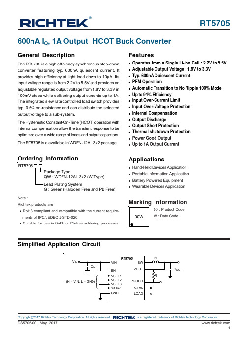
RT5705®DS5705-00 May 20171©Copyright 2017 Richtek Technology Corporation. All rights reserved. is a registered trademark of Richtek Technology Corporation.Simplified Application Circuit600nA I Q , 1A Output HCOT Buck ConverterGeneral DescriptionThe RT5705 is a high efficiency synchronous step-down converter featuring typ. 600nA quiescent current. It provides high efficiency at light load down to 10μA. Its input voltage range is from 2.2V to 5.5V and provides an adjustable regulated output voltage from 1.8V to 3.3V in 100mV steps while delivering output currents up to 1A.The integrated slew rate controlled load switch provides typ. 0.6Ω on-resistance and can distribute the selected output voltage to a sub-system.The Hysterestic Constant-On-Time (HCOT) operation with internal compensation allow the transient response to be optimized over a wide range of loads and output capacitors.The RT5705 is a available in WDFN-12AL 3x2 package.Features●Operates from a Single Li-ion Cell : 2.2V to 5.5V ●Adjustable Output Voltage : 1.8V to 3.3V ●Typ. 600nA Quiescent Current ●PFM Operation●Automatic Transition to No Ripple 100% Mode ●Up to 94% Efficiency●Input Over-Current Limit●Input Over-Voltage Protection ●Internal Compensation ●Output Discharge●Output Short Protection●Thermal shutdown Protection ●Power Good Output ●Up to 1A Output CurrentApplications●Hand-Held Devices Application ●Portable Information Application ●Battery Powered Equipment ●Wearable Devices ApplicationOrdering InformationNote :Richtek products are :❝ RoHS compliant and compatible with the current require-ments of IPC/JEDEC J-STD-020.❝ Suitable for use in SnPb or Pb-free soldering processes.Marking InformationRT5705G : Green (Halogen Free and Pb Free)00 : Product CodeW : Date CodeVRT57052DS5705-00 May 2017©Copyright 2017 Richtek Technology Corporation. All rights reserved. is a registered trademark of Richtek Technology Corporation.Functional Pin DescriptionPin Configuration(TOP VIEW)WDFN-12AL 3x2SW GND VSEL1VSEL2VIN EN VOUT VSEL3VSEL4CTRL PGOODLOADRT57053DS5705-00 May 2017©Copyright 2017 Richtek Technology Corporation. All rights reserved. is a registered trademark of Richtek Technology Corporation.Functional Block DiagramOperationThe RT5705 is a hysteretic constant on/off time (HCOT)switching buck converter, designed to an adjustable output voltage from an input supply voltage. The inductor current is regulated by a fast current regulator which is controlled by a voltage control loop. The voltage error amplifier getsits feedback input from the FB pin. The output voltage of the RT5705 is adjustable via SEL1 to SEL4 pins. When VIN is closed to VOUT , the device entering bypass mode with seamless technique and keep a minimum current ripple in the inductor to guarantee good performance.Absolute Maximum Ratings (Note 1)●Supply Input Voltage----------------------------------------------------------------------------------------------------0.3V to 5.5V●Power Dissipation, P D @ T A= 25°CWDFN-12AL 3x2--------------------------------------------------------------------------------------------------------- 3.17W●Package Thermal Resistance (Note 2)WDFN-12AL 3x2, θJA--------------------------------------------------------------------------------------------------- 31.5°C/W WDFN-12AL 3x2, θJC--------------------------------------------------------------------------------------------------- 6°C/W●Lead Temperature (Soldering, 10 sec.)----------------------------------------------------------------------------- 260°C●Junction T emperature Range------------------------------------------------------------------------------------------ 150°C●Storage T emperature Range------------------------------------------------------------------------------------------- −65°C to 150°C ●ESD Susceptibility (Note 3)HBM (Human Body Model)-------------------------------------------------------------------------------------------- 2kVRecommended Operating Conditions (Note 4)●Supply Input Voltage---------------------------------------------------------------------------------------------------- 2.7V to 4.5V●Junction T emperature Range------------------------------------------------------------------------------------------ −40°C to 125°C ●Ambient T emperature Range------------------------------------------------------------------------------------------ −40°C to 85°CElectrical Characteristics(V IN= 3.6V, C IN= 10μF, C OUT = 10μF, T A= 25°C unless otherwise specified)Note 1. Stresses beyond those listed “Absolute Maximum Ratings” may cause permanent damage to the device. These are stress ratings only, and functional operation of the device at these or any other conditions beyond those indicated in the operational sections of the specifications is not implied. Exposure to absolute maximum rating conditions may affect device reliability.Note 2.θJA is measured under natural convection (still air) at T A= 25°C with the component mounted on a high effective-thermal-conductivity four-layer test board on a JEDEC 51-7 thermal measurement standard. θJC is measured at the exposed pad of the package.Note 3. Devices are ESD sensitive. Handling precaution is recommended.Note 4. The device is not guaranteed to function outside its operating conditions.RT57056DS5705-00 May 2017 ©Copyright 2017 Richtek Technology Corporation. All rights reserved. is a registered trademark of Richtek Technology Corporation.Typical Application CircuitTable 1. Output Voltage SettingRT57057DS5705-00 May 2017©Copyright 2017 Richtek Technology Corporation. All rights reserved. is a registered trademark of Richtek Technology Corporation.Non-Switch Quiescent Current0.00.10.20.30.40.50.60.70.80.91.02.02.53.03.54.04.55.05.5Input Voltage (V)Q u i e s c e n t C u r r e n t ( A )Output Ripple Voltage010203040506070800.00.20.40.60.81.0Input Voltage (V)V O U T P P P e a k t o P e a k O u t p u t R i p p l e (m V )Output Ripple Voltage 051015202530354045500.00.20.40.60.81.0Input Voltage(V)V O U T P P P e a k t o P e a k O u t p u t R i p p l e (m V )Switch Frequency0.00.20.40.60.81.01.21.41.61.82.00.00.20.40.60.81.0Output Current (A)F r e q u e n c y (M H Z )Switch Frequency0.00.20.40.60.81.01.21.41.61.82.00.00.20.40.60.81.0Output Current (A)F r e q u e n c y (M H Z )Typical Operating CharacteristicsShutdown Current0.000.050.100.150.202.02.53.03.54.04.55.05.5Input Voltage (V)Q u i e s c e n t C u r r e n t ( A )μμRT57058DS5705-00 May 2017 ©Copyright 2017 Richtek Technology Corporation. All rights reserved. is a registered trademark of Richtek Technology Corporation.Line Regulation3.203.253.303.353.403.453.33.84.34.85.35.8Input Voltage (V)O u t p u t V o l t a g e (V )Line Regulation1.771.791.811.831.851.872.22.73.23.74.24.75.2 5.76.2Input Voltage (V)O u t p u t V o l t a g e (V )Line Reg Pass Through2.002.052.102.152.202.252.302.352.402.202.252.302.352.402.452.50Input Voltage (V)O u t p u t V o l t a g e (V )Efficiency1020304050607080901000.0000010.00010.011I OUT (A)E f f i c i e n c y (%)Line Reg Pass Through2.42.52.62.72.82.93.02.42.52.62.72.82.9Input Voltage (V)O u t p u t V o l t a g e (V )Line Reg Pass Through3.23.33.43.53.63.73.8Input Voltage (V)O u t p u t V o l t a g e (V )RT57059DS5705-00 May 2017©Copyright 2017 Richtek Technology Corporation. All rights reserved. is a registered trademark of Richtek Technology Corporation.V OUT Ripple VoltageTime (4ms/Div)V IN = 3.6V, V OUT = 1.8V, I OUT = 10μA, Ctrl = LV OUT(20mV/Div)LX (2V/Div)Time (40μs/Div)V IN = 4.5V, V OUT = 3.5V,I OUT = 0A to 2ATime (1μs/Div)I LX(200mA/Div)V OUT (20mV/Div)LX (2V/Div)I LX(200mA/Div)V IN = 3.6V, V OUT = 1.8V, I OUT = 10mA, Ctrl = LV OUT(20mV/Div)LX (2V/Div)I LX(200mA/Div)V IN = 3.6V , V OUT = 1.8V, I OUT = 500mA, Ctrl = LEfficiency0.0000010.00010.011I OUT (A)Load Regulation1.701.751.801.851.901.950.0000010.00010.011I OUT (A)O u t p u t V o l t a g e (V )Load Regulation0.0000010.00010.011I OUT (A)RT570510DS5705-00 May 2017 ©Copyright 2017 Richtek Technology Corporation. All rights reserved. is a registered trademark of Richtek Technology Corporation.V OUT Ripple VoltageTime (1μs/Div)V OUT(20mV/Div)LX (2V/Div)I LX(200mA/Div)V IN = 3.6V, V OUT = 1.8V, I OUT= 1A, Ctrl = LTime (5ms/Div)V OUT (20mV/Div)LX (4V/Div)I LX(500mA/Div)V IN = 3.6V, V OUT = 1.8V ,I OUT = 0A to 2A, Ctrl = LLoad TransientTime (50μs/Div)V OUT(50mV/Div)I OUT(100mA/Div)Load TransientTime (50μs/Div)Time (50μs/Div)Time (50μs/Div)Load_V (50mV/Div)Load_I (50mA/Div)I OUT(200mA/D iv)V IN = 3.6V, V OUT = 1.8V, t R = t F = 1μs,I OUT = 0mA to 150mA, Ctrl = LV OUT (50mV/Div)I OUT(200mA/Div)V IN = 3.6V , V OUT = 1.8V , t R = t F = 1μs,I OUT = 0mA to 300mA, Ctrl = LV OUT(100mV/Div)I OUT(500mA/Div)V IN = 3.6V, V OUT = 1.8V , t R = t F = 1μs,I OUT = 0A to 1A, Ctrl = LV OUT (50mV/Div)V IN = 3.6V , V OUT = 1.8V , t R = t F = 1μs,I OUT = 0mA to 100mA, Ctrl = HDS5705-00 May 2017©Copyright 2017 Richtek Technology Corporation. All rights reserved. is a registered trademark of Richtek Technology Corporation.Time (400μs/Div)V OUT(500mV/Div)PG (2V/Div)I LX(200mA/Div)V IN = 3.6V , V OUT = 1.8V ,I OUT= 0A, Ctrl = LTime (400μs/Div)Power Off ENTime (100μs/Div)V IN = 3.6V, V OUT = 1.8V,I OUT = 0A, Ctrl = LPower Off ENTime (20μs/Div)V IN = 3.6V, V OUT = 1.8V ,I OUT= 1A, Ctrl = LTime (500μs/Div)Load (500mV/Div)I LX(200mA/Div)V IN = 3.6V , V OUT = 1.8V ,I OUT = 0A, I OUT_LSW = 0A,Ctrl = HTime (500μs/Div)V EN (2V/Div)V OUT(500mV/Div)PG (2V/Div)I LX(500mA/Div)V EN (2V/Div)V IN = 3.6V, V OUT = 1.8V,I OUT = 1A, Ctrl = LV OUT(500mV/Div)PG (2V/Div)I LX(200mA/Div)V EN (2V/Div)V OUT(500mV/Div)PG (2V/Div)I LX(500mA/Div)V EN (2V/Div)V OUT(500mV/Div)PG (2V/Div)V IN = 3.6V, V OUT = 1.8V,I OUT = 1A, I OUT_LSW = 0A,Ctrl = HLoad (500mV/Div)I LX(500mA/Div)V OUT(500mV/Div)PG (2V/Div)©Copyright 2017 Richtek Technology Corporation. All rights reserved. is a registered trademark of Richtek Technology Corporation.Time (100μs/Div)Time (10μs/Div)Dynamic VSELTime (600μs/Div)VSEL (2V/Div)I LX (1A/Div)V IN = 3.6V, V OUT = 1.8V to 3.3V ,I OUT = 5mA, Ctrl = LInput Voltage Ramp Up/DownTime (20ms/Div)I LX(200mA/Div)V IN = 0V to 5V,V OUT = 1.8V,I OUT = 5mA, Ctrl = LTime (20ms/Div)Load (500mV/Div)I LX(100mA/Div)V OUT(500mV/Div)PG (2V/Div)V IN = 3.6V, V OUT = 1.8V ,I OUT = 0A, I OUT_LSW = 0A,Ctrl = HLoad (500mV/Div)I LX(100mA/Div)V OUT(500mV/Div)PG (2V/Div)V IN = 3.6V, V OUT = 1.8V ,I OUT = 1A, I OUT_LSW = 0A,Ctrl = HPG (1V/Div)V OUT(500mV/Div)V EN (1V/Div)V IN = 0V to 5V,V OUT = 3.3V,I OUT = 5mA, Ctrl = LV OUT (1V/Div)I LX(200mA/Div)V EN (1V/Div)V OUT(500mV/Div)DS5705-00 May 2017©Copyright 2017 Richtek Technology Corporation. All rights reserved. is a registered trademark of Richtek Technology Corporation.Application InformationThe RT5705 is a synchronous low voltage step-down converter that can support the input voltage range from 2.2V to 5.5V and the output current can be up to 1A.Internal compensation are integrated to minimize external component count. Protection features include over current protection, under voltage protection and over temperature protection.UVLO ProtectionTo protect the chip from operating at insufficient supply voltage, the UVLO is needed. When the input voltage of VIN is lower than the UVLO falling threshold voltage, the device will be lockout.EnableThe device can be enabled or disenabled by the EN pin.When the EN pin is higher than the threshold of logic high, the device starts operation with soft-start. Once the EN pin is set at low, the device will be shut down. In shutdown mode, the converter stops switching, internal control circuitry is turned off, and the load is disconnected from the input. This also means that the output voltage can drop below the input voltage during shutdown.Output Voltage SettingThe RT5705 doesn’t require an external resistor divider to program the output voltage. The device by the pins VSEL 1-4. The RT5705 supports an output voltage range of 1.8V to 3.3V in 100mV steps. The output voltage can be changed during operation and supports a simple dynamic output voltage scaling, shown .The output voltage is programmed according to table Table 1.Power GoodWhen the output voltage is higher than PG rising threshold,the PG flag is High.CTRL with Load SwitchThe CTRL pin set to high, the LOAD pin is connected to the VOUT pin via an load switch and can power up an additional, provide sub-system used .If CTRL pin is pulled to GND, the LOAD pin is disconnected from the VOUT pin and internally connected to GND by an internal discharge switch.Inductor SelectionThe recommended power inductor is 2.2μH with over 1.6A saturation current rating. In applications, need to select an inductor with the low DCR to provide good performance and efficiency.C IN and C OUT SelectionThe input capacitance, C IN , is needed to filter the trapezoidal current at the source of the top MOSFET . To prevent large ripple voltage, a low ESR input capacitor sized for the maximum RMS current should be used. RMS current is given by :This formula has a maximum at V IN = 2V OUT , where I RMS =I OUT /2. This simple worst-case condition is commonly used for design because even significant deviations do not offer much relief. Choose a capacitor rated at a higher temperature than required.Several capacitors may also be paralleled to meet size or height requirements in the design.The selection of C OUT is determined by the Effective Series Resistance (ESR) that is required to minimize voltage ripple and load step transients, as well as the amount of bulk capacitance that is necessary to ensure that the control loop is stable. Loop stability can be checked by viewing the load transient response as described in a later section.The output ripple, ΔV OUT, is determined by :⨯OUT RMS OUT(MAX)IN V I = I 1V ⎡⎤∆≤∆⎢⎥⨯⨯⎣⎦OUT L OUT 1V I ESR + 8f C©Copyright 2017 Richtek Technology Corporation. All rights reserved. is a registered trademark of Richtek Technology Corporation.Thermal ConsiderationsThe junction temperature should never exceed the absolute maximum junction temperature T J(MAX), listed under Absolute Maximum Ratings, to avoid permanent damage to the device. The maximum allowable power dissipation depends on the thermal resistance of the IC package, the PCB layout, the rate of surrounding airflow,and the difference between the junction and ambient temperatures. The maximum power dissipation can be calculated using the following formula :P D(MAX) = (T J(MAX) − T A ) / θJAwhere T J(MAX) is the maximum junction temperature, T A is the ambient temperature, and θJA is the junction-to-ambient thermal resistance.For continuous operation, the maximum operating junction temperature indicated under Recommended Operating Conditions is 125°C. The junction-to-ambient thermal resistance, θJA , is highly package dependent. For a WDFN-12AL 3x2 package, the thermal resistance, θJA , is 31.5°C/W on a standard JEDEC 51-7 high effective-thermal-conductivity four-layer test board. The maximum power dissipation at T A = 25°C can be calculated as below :P D(MAX) = (125°C − 25°C) / (31.5°C/W) = 3.17W for a WDFN-12AL 3x2 package.The maximum power dissipation depends on the operating ambient temperature for the fixed T J(MAX) and the thermal resistance, θJA . The derating curves in Figure 1 allows the designer to see the effect of rising ambient temperature on the maximum power dissipation.Figure 1. Derating Curve of Maximum Power Dissipation0.00.40.81.21.62.02.42.83.23.64.0255075100125Ambient Temperature (°C)M a x i m u m P o w e r D i s s i p a t i o n (W )Layout ConsiderationsSome PCB layout guidelines for optimal performance of the RT5705 list as following.Following figure shows the real PCB layout considerations and it is based on the real component size whose unit is millimeter (mm).❝The input capacitor should be placed as closed as possible to PVIN pin for good filtering.❝The high current path should be made as short and wide as possible.❝The inductor should be placed as close to LX1 and LX2pin for reducing EMI.❝The output capacitor should be placed as closed as PGND pin to ground plane to reduce noise coupling.DS5705-00 May 2017©Copyright 2017 Richtek Technology Corporation. All rights reserved. is a registered trademark of Richtek Technology Corporation.Figure 2. PCB Layout GuideW-Type 12AL DF N 3x2 PackageRichtek Technology Corporation14F, No. 8, Tai Yuen 1st Street, Chupei CityHsinchu, Taiwan, R.O.C.Tel: (8863)5526789Richtek products are sold by description only. Richtek reserves the right to change the circuitry and/or specifications without notice at any time. Customers should obtain the latest relevant information and data sheets before placing orders and should verify that such information is current and complete. Richtek cannot assume responsibility for use of any circuitry other than circuitry entirely embodied in a Richtek product. Information furnished by Richtek is believed to be accurate and reliable. However, no responsibility is assumed by Richtek or its subsidiaries for its use; nor for any infringements of patents or other rights of third parties which may result from its use. No license is granted by implication or otherwise under any patent or patent rights of Richtek or its subsidiaries.。
Everlight IR15 -21C TR8 红外LED数据手册说明书

1 1206 Package Chip Infrared LED IR15-21C/TR8Features․Small double-end package ․High reliability․Low forward voltage․Good spectral matching to Si photodetector ․Pb free․The product itself will remain within RoHS compliant version. ․Compliance with EU REACHDescriptions․IR15-21C/TR8 is an infrared emitting diode in miniature SMD package which is molded in a water clear plastic With flat top view lens.․The device is spectrally matched with silicon photodiode and phototransistor.Applications․PCB mounted infrared sensor․Infrared emitting for miniature light barrier ․Floppy disk drive․Optoelectronic switch ․Smoke detector2Package DimensionsNotes: 1.All dimensions are in millimeters2.Tolerances unless dimensions ±0.1mm3.Suggested pad dimension is just for reference onlyPlease modify the pad dimension based on individual need3Notes: *1: Soldering time ≦5 seconds.45Typical Electro-Optical Characteristics Curves6 Precautions For Use1. Over-current-proofCustomer must apply resistors for protection, otherwise slight voltage shift will cause big current change (Burn out will happen). 2. Storage2.1 Do not open moisture proof bag before the products are ready to use.2.2 Before opening the package, the LEDs should be kept at 10℃~30℃ and 90%RH or less. 2.3 The LEDs suggested be used within one year.2.4 After opening the package, the devices must be stored at 10°C~30°C and 60%RH, and usedwithin 168 hours (floor life). If unused LEDs remain, it should be stored in moisture proof packages.2.5 If the moisture absorbent material (desiccant material) has faded or unopened bag hasexceeded the shelf life or devices (out of bag) have exceeded the floor life, baking treatment is required.2.6 If baking is required, refer to IPC/JEDEC J-STD-033 for bake procedure or recommend the following conditions:96 hours at 60°C ± 5°C and < 5 % RH (reeled/tubed/loose units) 3. Soldering Condition3.1 Pb-free solder temperature profile3.2 Reflow soldering should not be done more than two times. 3.3 When soldering, do not put stress on the LEDs during heating. 3.4 After soldering, do not warp the circuit board.7 4.Soldering IronEach terminal is to go to the tip of soldering iron temperature less than 350℃ for 3 seconds within once in less than the soldering iron capacity 25W. Leave two seconds and more intervals, and do soldering of each terminal. Be careful because the damage of the product is often started at the time of the hand solder. 5.RepairingRepair should not be done after the LEDs have been soldered. When repairing isunavoidable, a double-head soldering iron should be used (as below figure). It should be confirmed8Note : The tolerances unless mentioned are ±0.1mm, Unit: mm9 Label Form SpecificationCPN: Customer’s Production Number P/N : Production Number LOT No: Lot Number QTY: Packing Quantity HUE: Peak Wavelength CAT: RanksREF: Reference MSL-X: MSL LevelMade In: Manufacture placeNotes1. Above specification may be changed without notice. EVERLIGHT will reserve authority on material change for above specification.2. The graphs shown in this datasheet are representing typical data only and do not show guaranteed values.3. When using this product, please observe the absolute maximum ratings and the instructionsforuse outlined in these specification sheets. EVERLIGHT assumes no responsibility for any damage resulting from use of the product which does not comply with the absolute maximum ratings and the instructions included in these specification sheets.4. These specification sheets include materials protected under copyright of EVERLIGHT. Reproduction in any form is prohibited without the specific consent of EVERLIGHT.5. This product is not intended to be used for military, aircraft, automotive, medical, life sustaining or life saving applications or any other application which can result in human injury or death.Please contact authorized Everlight sales agent for special application request.。
APT7L05电容式触摸传感器数据手册说明书

APT7L05电容式触摸传感器数据手册1概述1.1APT7L05电容触摸传感器简述APT7L05是一款5通道多用途的电容触摸传感器,适合任何形式的触摸按键控制。
APT7L05采用直通形式,可以方便快捷地取替传统机械按键。
1.2特征◆电容触摸按键:5通道(每一通道独立工作);◆抗干扰能力强:可抵抗5W大功率对讲机测试,有效防止水滴;◆灵敏度:适合面板厚度在5mm以内的应用。
灵敏度调节详见参考电路(本手册第10页);◆输出模式:直通模式或锁存翻转模式可选(详见OM端口说明);◆上电后默认输出电平高低可选(详见OL端口说明);◆低功耗:工作电流为45uA@5V◆内置LDO:提高抗噪性能,并减少系统成本;◆工作温度:–40︒C到+85︒C;◆工作电压:2.2V到5.5V;◆封装及型号:QFN16(APT7L05NF)、SOP16(APT7L05SF)、SSOP16(APT7L05VF)。
1.3管脚分配图1-3-2APT7L05管脚分配(SOP16/SSOP16)图1-3-1APT7L05管脚分配(QFN16)1.4管脚功能说明表1-4APT7L05管脚说明管脚名称说明QFN16管脚位SOP16/ SSOP16管脚位C0外部电容:10nF(103)13K<4:0>触摸按键输入(不使用时必须悬空)2-64-8 O<4:0>对应触摸按键K<4:0>的输出7-119-13SS全局灵敏度输入控制脚,默认上拉;当接地时,灵敏度提高。
1214OL 接地时,O<4:0>默认输出高电平,当K<4:0>按下时输出低电平;悬空或接VDD时,O<4:0>默认输出低电平,当K<4:0>按下时输出高电平;1315OM 接地时为锁存翻转模式:当K<4:0>按下时,对应O<4:0>输出电平改变并保持(即使松开按键),当下一次按下时,对应O<4:0>输出电平翻转并保持(即使松开按键);悬空接VDD时为直通模式:当K<4:0>按下时,对应O<4:0>输出电平改变,松开K<4:0>时,对应O<4:0>输出电平恢复默认状态;162V DD芯片电源脚1416 V SS芯片地1512电气特性2.1极限参数表2-1极限参数(TA=25︒C)参数标号对象范围单位电源供电电压VDD––0.3to+6.5V端口输入电压VI所有端口–0.3to VDD+0.3V端口输出电压VO所有端口–0.3to VDD+0.3V高电平输出电流IOH单个口–10mA所有口–40mA低电平输出电流IOL单个口+20(峰值)mA所有口+60(峰值)mA工作温度TA––40to+85°C储藏温度TSTG––65to+150°C 2.2直流电气特性表2-2直流电器特性(TA=–40︒C~85︒C,VDD=2.2V~5.5V)参数标号条件最小典型最大单位工作电压VDD-- 2.2 5.5V 输出高电平VOH IOH=–10mA VDD=2.2to5.5V VDD-1.0-VDD V 输出低电平VOL IOL=20mA VDD=2.2to5.5V–- 1.0V输出高电平漏电流ILOH-VOUT=VDD––1uA输出低电平漏电流ILOL-VOUT=0V–––1uA供电电流IDD1工作模式VDD=2.2to5.5V–4560uA2.3交流电气特性表2-3交流电气特性(TA=–40︒C~85︒C,VDD=2.2V~5.5V)参数符号条件最小值典型值最大值单位输入电容CIN f=1MHz;不测试的管脚接地10pF输出电容COUT I/O口电容CIO3封装尺寸APT7L05采用QFN16,SOP16及SSOP16封装。
LPA2171-00中文版和8871通用

5.5
Supply Voltage ( V )
Supply Voltage ( V )
OUTPUT POWER vs SUPPLY VOLTAGE
6.0 5.4 4.8
OUTPUT POWER vs SUPPLY VOLTAGE 3.5 RL=4Ω+33μH f=1kHz THD+N=10%
RL=2Ω+33μH f=1kHz THD+N=10%
VDD=3.6V
VDD=3.6V
VDD=5V -90 20 100 1K FREQUENCY ( Hz ) 10K 20K -75 20 100
VDD=5V 1K FREQUENCY ( Hz ) 10K 20K
Copyright@LOWPOWER Semiconductor
10 0 0 0.4 0.8
RL=4Ω+33μH 1.2 1.6 2.0 2.4 Output Power ( W ) 2.8 3.2
THD+N vs OUTPUT POWER 100 RL=2Ω+33μH f=1kHz 10 VDD=2.5V VDD=3.6V 10 100
THD+N vs OUTPUT POWER
5
5.5
Supply Voltage ( V )
Copyright@LOWPOWER Semiconductor
page7
Nov,2012 Rev.1.0
LPA2171
、 AB LPA2171 FM D , 。 5V 5.2W 2Ω 5.5 W , 90% 。 LPA2171 AERC (( Adaptive Edge Rate , Control ) EMI , 60 cm , FCC 20 dB 。 P WM LPA2171 D , PCB , 。 , , , , , LPA2171 。
IRPT 红外测温仪 数据手册说明书

输出模拟输出数字输出 0-20mA,4-20mA,0-5V RS485可调参数发射率激光器控制工作模式响应时间工作电源±0% 500mA24VDC 2防护等级 IP65工作温度 风冷 水冷110 无冷却0-65165℃℃ ℃存储温度 -20-70℃相对湿度10 - 95%, 无结露抗冲击 GB/T2423.1,GB/t2423.2抗扰标准 JB/T9233.11-1999重量 478g外形尺寸L:max138mm; 50mm Φ 重复性精度± 0.2% 温度分辨力 ℃ 0.5 响应时间 ≤5ms发射率调整 0.10 to 1.00 (0.01)IRPT IRPT LED IRPT 0.8~1510m IRPT 是一款通用型红外测温仪。
体积小巧,测量速度快,环境适应能力强。
可以应用于环境恶劣的、粉尘、高温环境热工温度检测。
红外测温仪是工业温度测量的又一理想选择。
通过仪表显示及人工交互面板,实现瞄准激光控制,测量误差校正,测量模式选择,测量速度调整等操作。
高亮显示当前测量值。
调试简单,安装方便。
可以实现远距离测量,当测量距离在米之间变化,测量值不变,所以对于测量距离大于以上的温度测量场合,尤其适用。
该产品在轧钢行业实现对高速移动目标温度准确测量,并组网,配合DIKAI V30 .数据采集软件实现测量及数据记录分析等功能。
适用领域:轧钢、高速线材等高速移动目标;铸造、粉末冶金,化工,玻璃、陶瓷生产,热处理,焦化,热压烧结,焊接等行业,以及无法近距离测量的高危场合。
IRPTL1 45:1 3mm@210mm IRPTL2 45:1 3mm@210mm IRPTL3 120:1 3mm@360mm IRPTH1 200:1 3mm@600mm IRPTH2 200:1 3mm@600mm测量精度IRPTL1,IRPTL2,IRPTL31%(FS)IRPTH1,IRPTH20.5%(FS)±±探测器IRPTL1, IRPTL2 Thermopile 8-14µmIRPTL3 InGaAs 2-2.5µm IRPTH1, IRPTH2 InGaAs 0.7-1.7µm量程范围IRPTL1 -30-650IRPTL2-25-800IRPTL3100-600IRPTH1 500-1400IRPTH2 650-1650℃℃℃℃℃可测最小目标和测量距离参数型号:可测最小目标DS安装支架外形尺寸距离:传感器距目标距离()in 距离:传感器距目标距离()mm 距离:传感器距目标距离()in 距离:传感器距目标距离()mm 距离:传感器距目标距离()in 距离:传感器距目标距离()mm 有偿服务选项可选配件RS232/485转换链接器风冷套/水冷套镜头防尘空气吹扫器耐高温电缆线(并注明长度)显示变送仪表上位机软件用户在购买之前确定以下选项显示变送仪表中国国家计量主管部门出具的校准证书中国国家计量主管部门出具的标定证书。
- 1、下载文档前请自行甄别文档内容的完整性,平台不提供额外的编辑、内容补充、找答案等附加服务。
- 2、"仅部分预览"的文档,不可在线预览部分如存在完整性等问题,可反馈申请退款(可完整预览的文档不适用该条件!)。
- 3、如文档侵犯您的权益,请联系客服反馈,我们会尽快为您处理(人工客服工作时间:9:00-18:30)。
IR2175(S)&(PbF) 线性电流感应IC 数据手册
NO. PD60208 Rev.E
特点
Floating 通道最大电压+600V 单片集成
通过分流电阻进行线性电流反馈 直接数字输出、接口简单 低IQBS ,允许自举电路供电 独立过流保护信号 高共模抗噪音
输入过压保护(IGBT 短路电流) 漏极开路输出 无铅制程
描述
IR2175是专为电机驱动设计的单片电流感应IC 。
它通过外接分流电阻测量电机相电流,把模拟信号转换为数字信号,并把该信号输送到低边。
IR 的高压隔离专利技术可以处理高带宽的信号。
输出离散PWM 而不需A/D 输入接口。
过流信号可以使IGBT 短路保护。
漏极开路输出适应3.3V 到15V 电压。
模块图
封装
极限额定值
超过极限额定值可能发生错误或者损坏,所有的电压参数是以COM为参考的绝对数值。
所有电流值定义为正值。
热阻和功耗是在空气静止的环境下在电路板上测得的。
推荐操作条件
图一为输出逻辑时序。
设备需工作在推荐操作条件下。
直流电气特性
注释2:Gain=最大占空比/最大输入电压交流电气特性
图一输出波形时序
提示:
同时测量PWM周期和PWM有效时间可以消除输出载波频率的温漂。
因为他们是同向波动的。
在每一个周期计算它们的比值可以获得消除温漂的测量值。
引脚定义
引脚分布
外形尺寸
IR2175应用指南AN-1052
1 基本功能
本段说明IR2175的基本操作.该IC把高边的电机驱动电流转换到低边。
模拟输入的电压信号实际上是外接感应电阻的压降。
这个电阻感应电机相电流并产生一个很小的交流电压信号。
最大输入信号为260mV。
所以电阻应选择使电压在260mV以内的值,使过流信号电压达到260mV(如10A过流信号选择26mΩ电阻)。
交流输入信号通过IC转换为PWM信号,高边载波频率为130KHz,然后降低PWM电平到低边的参考电平。
PO输出是漏极开路输出,操作电压3.3V到15V。
PO脚需上拉电阻接电源,该上拉电阻典型值为1~10K。
有两种方式处理IR2175的输出信号:
1、用滤波器滤掉载波频率输出模拟信号
2、直接输出数字信号,通过软件算法计算电流
第3、4段会详细说明
Vb和Vs之间的高边浮动电压由自举电路产生,下一段详细说明。
Vbs电压最小8V,推荐Vbs和Vcc电压都在10V以上。
2 自举电路
Vbs电压是建立在Vs电压之上(大部分是高频方波)。
有几种发法可以产生Vbs,一种是自举电路,这个方法简单廉价,但是有一些限制。
占空比和开通时间限制自举电路的充电(长开通时间和高占空比需要充电泵电路,参考AN978)自举电路由二极管和电容组成,见数据手册的模块图。
电路工作方式如下。
当Vs被拉到地,自举电容通过自举二极管从15V Vcc充电。
当Vs被高边拉高时,自举二极管反偏。
略
4 输出信号的数字接口
连接到DSP或者MCU的硬件电路简单得多,大
部分工作都由软件算法来完成。
而且,这种方法不会
带来滤波电路产生的错误信号。
IR2175主要就是为这
种数字应用设计的。
4.1 硬件接口
PO为漏极开路输出,可以从DSP和MCU的3.3V
或者5V电源接上拉电阻。
见右图。
4.2 PWM信号的软件解码
与DSP的典型应用见DT99-8,这是一个TI TM320C240和IR2171/IR2172的硬件电路和软件解决方案
5 Vs引脚瞬态反向的处理
注意:和门极驱动信号不同步,电流感应IC需要自己的瞬态反向保护电路。
和门极驱动信号不同,电流感应IC是持续工作的,必须确保Vs引脚不产生反向。
更多细节可以参考
DT97-3。
注意典型连接里面有一个com 到Vs 的二极管和一个在Vs 和半桥中点之间的电阻,这两个元件使Vs 最多跌落com 一个二极管压降。
这个二极管必须是快速恢复的,最好是小于100ns 的1A 二极管,电阻范围10~20Ohms 。
尽管这个Vs 和半桥中点之间的电阻在电流感应回路中,但是不会影响电流感应信号,因为这个电阻没有电流流过。
只有在transition 发生时,才有持续时间很短的电流。
由于有限的slew rate ,IR2175的输入端放大器会忽略这个短暂的信号。
6 布局建议
功率器件需减少寄生效应。
图九为典型的半桥电路和杂散电感。
每个杂散电感的连线需尽可能宽且短。
IR2175的注意事项和那些门极驱动IC 一样,如图10,退耦电容需尽可能贴近IC 。
V-和Vs 得连线也要尽可能贴近IC 以消除压差。
感应电阻和V+连线尽可能短以减小噪音。
图11给出一个IR2175的布局实例。
注意感测电阻和IC 连接越短越有利于消除电流感应信号的噪音。
大电流走线尽量宽以消除电感。
R2和D2组成的瞬态反向保护电路贴近IC 以产生最大的效果。
注意退耦电容需尽可能贴近IC 的引脚。
7 DV/DT 和对占空比的作用
这也被叫做CMRR (共模抑制比)。
高边是浮动的但是没有开关状态(如Vs 引脚电压固定),将不会产生占空比抖动。
然而在使用两个IC 测量三相电流中的两相这个应用中,Vs 脚在地、近地、直流母线之间转换,每次转换会产生一个dV/dt ,对PO 脚的输出占空比会产生轻微抖动。
直流母线300V 时IR2175的抖动为2%,表一给出不同的母线电压下,IR2171/2和IR2175的dV/dt 。
这个结果是从一个IR 的伺服系统测得的。
电机驱动电路中,这个dV/dt 会转化为转矩波动,因此需要考虑到其影响。