Freescale S19文件格式
Freescale 半导体用户指南说明书
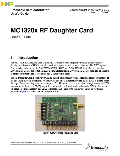
Freescale Semiconductor User’s GuideDocument Number: MC1320xRFCUGRev. 1.2, 03/20101IntroductionThe MC1320x RF Daughter Card (1320xRFD-A00) is used in conjunction with a microcontroller development board for RFIC evaluation, code development, and system evaluation. The RF Daughter Card interfaces directly to the M68EVB908GB60, RG60 and QG60 HCS08 family Microcontroller Development Boards and to the M52235 EVB Microcontroller Development Board, but it can be adapted to other boards that offer access to the MCU input/output ports.The RF Daughter Card is configured with all the off-chip circuitry required for functional performance of the MC1320x RF data modem except the MCU. The MCU interface required by the RFIC is pinned out at the edge of the card using standard header pins. The RF interface is accomplished through an onboard PCB antenna. Also, there is an SMT jumper that can be relocated, which will redirect the RF interface to an on-board 50 ohm connector. The SMA connector can be used with standard coax cables for testing purposes. Figure 1-1 shows the RF Daughter Card.Figure1-1. MC1320x RF Daughter CardMC1320x RF Daughter CardUser’s GuideIntroductionFigure1-2 shows the RF Daughter Card installed in a GB60 development board.Figure1-2. MC1320xRF Daughter Card In GB60 Development Board Figure1-3 shows the M52235 EVB development board.Figure1-3. M52235 EVB Development BoardSafety Information 2Safety InformationAny modifications to this product may violate the rules of the Federal Communications Commission and make operation of the product unlawful.47 C.F.R. Sec. 15.21This equipment has been tested and found to comply with the limits for a Class B digital device, pursuant to part 15 of the FCC Rules. These limits are designed to provide reasonable protection against harmful interference in a residential installation. This equipment generates uses and can radiate radio frequency energy and, if not installed and used in accordance with the instructions, may cause harmful interference to radio communications. However, there is no guarantee that interference will not occur in a particular installation. If this equipment does cause harmful interference to radio or television reception, which can be determined by turning the equipment off and on, the user is encouraged to try to correct the interference by one or more of the following measures:•Reorient or relocate the receiving antenna.•Increase the separation between the equipment and receiver.•Connect the equipment into an outlet on a circuit different from that to which the receiver is connected.•Consult the dealer or an experienced radio/TV technician for help.47 C.F.R. Sec.15.105(b)This equipment complies with FCC radiation exposure limits set forth for an uncontrolled environment. The antenna(s) used for this equipment must be installed to provide a separation distance of at least 8 inches (20cm) from all persons.This device complies with Part 15 of the FCC Rules. Operation is subject to the following two conditions:•This device may not cause harmful interference.•This device must accept any interference received, including interference that may cause undesired operation.3Revision HistoryThe following table summarizes revisions to this document since the previous release (Rev 1.1).Revision HistoryLocation RevisionSection 6Updated document cross reference.MC1320x MCU Interface4MC1320x MCU InterfaceFigure4-1 shows the typical connections between the MC1320x transceiver and a microcontroller unit (MCU). See the MC13202/203 Reference Manual, document MC13202RM, for interface considerations. Details about the interconnects for both the GB60 and M52235 Development boards are described in Section5.1, “Development Board Interconnects”. ArrayFigure4-1. MCU Interface PinoutDaughter Card Description 5Daughter Card DescriptionAs shown in Figure5-1 and Figure8-1, connector J101 is the main interface to the GB60 Development Board. The interface connections described in Section5.1, “Development Board Interconnects”, fall under the following three broad categories:1.Serial Peripheral Interface (SPI)2.Control3.PowerFigure1-2 shows how the RF Daughter Card is mounted on the GB60 Development Board.NOTEEnsure that zero ohm resistor R104 is in place on the MC1320x DaughterCard. As of this release, previous versions of the MC1320x Daughter Cardmay not have R104 inserted.NOTEJ101 Pin 1 of the MC1320x must to be connected to GB_PORT Pin 1 of theGB60 Development Board.As shown in Figure5-1 and Figure8-1, connector J102 is the main interface to the M52235 Development Board. Figure1-3 shows how the RF Daughter Card is mounted on the M52235 Development Board.NOTEJ102 Pin 1 of the MC1320x must be connected to MCU_PORT Pin 1 on theM52235 Development Board.Figure5-1 shows the top side of the RF Daughter Card PCB with component placement.Figure5-1. MC1320x Daughter Card (Top View)Daughter Card DescriptionFigure5-2 shows the shows the bottom side of the RF Daughter Card PCB.Figure5-2. MC1320x Daughter Card (Bottom View)5.1Development Board InterconnectsThe following sections describe the interconnects for both the GB60 and M52235 Development boards. Table5-1 lists the pin connections for J101 and Table5-2 lists the pin connections for J102.Table5-1. J101 Pin ConnectionsPin Number Pin Name Description Functionality1,2,3,4, 6,7,8,9, 10,11,12,15,16,17 18,21,23,25,26,28, 29, 30,33N/C No connection.5PTA2Connects to PTA2 on GB60.Provides a wakeup function to the MCU via Pin22 when jumper is installed between J103 pins1 and 2.13GPIO1Connects to General PurposeInput/Output 1 of MC1320X.When gpio_alt_en, Register 9, Bit 7 = 1, GPIO1 functions as an “Out of Idle” Indicator.14GPOI2Connects to General PurposeInput/Output 2 of MC1320X.When gpio_alt_en, Register 9, Bit 7 = 1, GPIO2 functions as a “CRC Valid” Indicator.Daughter Card Description19IRQConnects to IRQ pin of MC1320X.Allows the MC1320X to issue an IRQ to theMCU.20RESETOptionally connects to RESET of MC1320X when R101 or R102 are installed.Allows the MCU to reset the MC1320X.22PTE1/RXD1Connects to PTE1/RXD1 of GB60.Provides a wakeup function to the MCU via Pin5 when jumper is installed between J103 pins 1 and 2.24XCLK/16MHz Connects to CLKO of MC1320Xwhen jumper is installed between J103 pins 3 and 4.Provides reference based on MC1320X 16 MHz reference oscillator to the MCU.27PTC2/BAUD SEL Connect to PTC2/BAUD SEL ofGB60.31RXTXENConnect to RXTXEN of MC1320X.Allows the MCU to control the RXTXEN line ofthe MC1320X.32RESETConnects to RESET of MC1320X.Allows the MCU to reset the MC1320X.34PTD5/CESI/A TTN Connects to PTD5/CESI of GB60when R104 is installed. Connectdirectly to Pin 15 of J102.Allows the MCU to wake up the MC1320X from Doze or Hibernate.35MOSIConnect to MOSI of MC1320x.SPI36SPSCKConnect to SPICLK of the MC13201.SPI37CE Connect to CE of MC1320X.SPI38MISO Connects to MISO of MC1320X.SPI39V_INConnects the Daughter Card to the supply voltage output of the GB60 board.Provides supply voltage to the Daughter Card. Voltage must not exceed 16 Vdc. See Section 5.1.0.3, “Power Connections”.40GNDConnect ground on GB60 board to ground on Daughter Card.Table 5-1. J101 Pin Connections (continued)Pin NumberPin Name DescriptionFunctionalityDaughter Card DescriptionTable5-2. J102 Pin ConnectionsPin Number Pin Names Description Functionality 4, 5, 6, 7, 8, 11, 12, 14,16, 18, 22N/C No connection1V_IN Connects the Daughter Card to thesupply voltage output on theM52235EVB.Provides supply voltage to the Daughter Card. Voltage must not exceed 16 Vdc. See Section5.1.0.3, “Power Connections”.2IRQ Connects to IRQ pin of MC1320X.Allows the MC1320X to issue an IRQ to theMCU.3GND Connects the ground of the RFDaughter Card to the ground of theM52235EVB9GPIO1Connects to General PurposeInput/Output 1 of MC1320X.When gpio_alt_en, Register 9, Bit 7 = 1, GPIO1 functions as an “Out of Idle” Indicator.10GPOI2Connects to General PurposeInput/Output 2 of MC1320X.When gpio_alt_en, Register 9, Bit 7 =1, GPIO2 functions as a “CRC Valid” Indicator.13RESET Connects to RESET of MC1320Xand Pin 32 of J101.Allows the MCU to reset the MC1320X.15PTD5/CESI Connects to ATTN of MC1320Xand Pin 34 of J101.Allows the MCU to wake up the MC1320X from Doze or Hibernate.17MOSI Connects to MOSI of MC1320X.SPI19MISO Connects to MISO of MC1320X.SPI20RXTXEN Connect to RXTXEN of MC1320X.Allows the MCUntrol the RXTXEN line of theMC1320X.21SPICLK Connect to SPICLK of theMC1320XSPI23PTE2/CE-QSPI-CSO Connects to Pin 1 of J104Allows Chip Enable (CE) selection.See Section5.1.0.1, “SPI Connections”.24PTE2/CE-AN7Connects to Pin 3 of J104Allows Chip Enable (CE) selection.See Section5.1.0.1, “SPI Connections”.Daughter Card DescriptionNOTEIn the following sections, pin numbers not in parenthesis reference theGB60 Development Board. Pin numbers in parenthesis reference theM52235 Development Board.5.1.0.1SPI ConnectionsJ101 pins 35 through 38 (J102 pin 17, 19, 21 and 23) provide the following four wire SPI interface:•MOSI•SPICLK•CE•MISOThe MC1320x always functions as a slave device. SPI operation is described in detail in the appropriate MC1320x Data Sheet and/or MC1320x Reference Manual.NOTEAs it applies to the M52235 Development Board, the CE signal on (J102 Pin23 and Pin 24) are hard wired to header J104. These pins control thefunctionality of CE.When Pin 2 and Pin 3 of J104 are shorted, CE is wired to (J102 Pin 24)(PTE2/CE-AN7).When Pin 1 and Pin 2 of J104 are shorted, CE is wired to (J102 Pin 23)(PTE2/CE-QSPI_CS0).5.1.0.2Control Connections•J101 Pin 19 (J102 Pin 2) is the IRQ line from the MC1320x. Connection to the MCU depends on how the MCU services interrupts.•J101 Pin 31 (J102 Pin 20), RXTXEN, allows the MCU to initiate transceiver functions.•J101 Pin 34 (J102 Pin 15), ATTN, allows the MCU to wake up the MC1320x from Doze or Hibernate low power modes.NOTERXTXEN and ATTN are also available at header J105 for manual control.•J101 Pin 24 provides the MC1320x CLKO to the MCU when a jumper is installed at J103.•J101 Pin 32 (J102 Pin13) interfaces with the MCU to provide a Reset to the MC1320x.•J101 Pin 5 and Pin 22 provide a wake up function to the MCU when a jumper is installed at J103.•J101 Pin 13 and Pin 14 (J102 Pin 9 and Pin 11) provide access to the MC1320x GPIO1 and GPIO2 ports.RF Circuit5.1.0.3Power ConnectionsJ101 Pin 39 (J102 pin 1) provides the supply voltage to the RF Daughter Card. V oltage on this line should never exceed 16.0 VDC and the nominal voltage supply should not exceed 16.0 VDC. J101 Pin 40 (J102 pin 3) is ground.NOTEMCU connection signals are dependent on the on-board voltage regulator.If R105, D101, and C101 are mounted and R115 is removed, J101 Pin 39will provide the interface supply voltage which must never exceed 3.6 V.Nominal supply voltage should never exceed 3.4 V.5.1.0.4Non-MCU ConnectionsHeader J105 provides connections to a number of MC1320x contacts for non-MCU connections. As already stated, the RXTXEN and ATTN lines are available at J105 for external control using switches or other hardware. The MC1320x GPIO is also available for connection to external hardware.6RF CircuitThe MC1320x has an internal TX/RX switch. This feature allows for an external RF circuit that has a very low component count. The MC1320x requires only a few passive components and a balun to provide an interface to an antenna or a 50 ohm circuit. Figure6-1 shows a schematic for only the RF portion of the MC1320x Daughter Card.Figure6-1. RF Portion of 20x Daughter CardSoftware Configuration To provide a design that is of the lowest possible cost to produce, this reference design was built on a printed circuit board consisting of only two layers and with a printed circuit board antenna. The antenna is an Inverted F design widely used in the 2.4 GHz band. This antenna provides good performance while minimizing Bill of Material (BOM) cost.For more information on a low cost design approach, see the ZigBee Hardware Design Considerations Reference Manual (ZHDCRM)7Software ConfigurationAs shown in Figure8-1, the legend in the schematic shows the recommended jumper settings for Wake, ClkOut, and Chip Enable.NOTEThe Wake and ClkOut signals are only for interface to the GB60Development Board. The Chip Enable signal is only for interface to theM52235 Development Board.For software development, Freescale recommends users obtain the most recent software development tools and documentation from the following web pages:•For ZigBee related software and documentation go to /zigbee•For microcontroller software and documentation go to Bill of Materials (BOM) and Schematic8Bill of Materials (BOM) and Schematic This section contains the RF Daughter Card BOM and schematic.Table8-1. Bill of MaterialsQty Part Number ValueRatingToleranceManufacturer Part Number Reference196000310100Label 21*6mmTest BarCode96000310100BARCODE101350610710001100nF16V±10% X7R Murata GRM155R71C104KA88D C103, C104,C105050610710001100nF16V±10% X7R Murata GRM155R71C104KA88D C101 (NotMounted)2506208100011µF 6.3V±10% X5RMurata GRM188R60J105KA01D C102, C1060506208100011µF 6.3V±10% X5R Murata GRM188R60J105KA01D C108 (NotMounted)05061061000010nF16V±10% X7R Murata GRM155R71E103KZ01E C107(NotMounted)153300833001 3.3µF10V20%Vishay Sprague293D335X0010A2TE3C109250210268000 6.8pF50V±0.25pF NP0/C0GMurata GRM1555C1H6R8DZ01J C110, C11115021031000010pF50V±5% NP0/C0GMurata GRM1555C1H100JZ01D C112150210210000 1.0pF50V±0.25pF NP0/C0GMurata GRM1555C1H1R0CZ01D C113040110003303MM3Z3V3T1G 3.3V/200mW5%ONSemiconductorMM3Z3V3T1G D101 (NotMounted)141100017001Green_LED Citizen CL-170G-CD-T D102135501320200MC13202FreescaleSemiconductorMC13202IC101 134000298109LP2981IM5-3.3-40 to +125°C National LP2981IM5-3.3 NOPB IC1021200304040012*20p PinHeader - RightAnglemot/molex70216-4010-89-4402J1011200304024012*12p PinHeader - RightAnglemot/molex70216-2410-89-4242J1021200304004002*2p PinHeaderAMP0-826632-2J103 120030400300jumper_1x3AMP826629-3J104Bill of Materials (BOM) and Schematic200304020082*10 Pin HeaderAMP1-826632-0J105 (Not Mounted)120150700202SMA_edge_Re ceptacle_Fema lemot/sma-end_launch 142-0701-831J106220030000100ProbeLoop TobyElectronics TP-107-02-5-T J107, J108254710518001 1.8nH 300mA ±0.3nH TOKO LL1005-FHL1N8S L101, L102254710539002 3.9nH ±0.3nHTOKO LL1005-FHL3N9S L103, L104171000566010fsl566-1FreescaleSemiconductor FSL566-1 FR4 0.76mm PCB1014611000000010R 62.5mW/25V 5%YAGEO RC0402JRE070RL R103, R112, R115,R1040611000000010R62.5mW/25V 5%YAGEORC0402JRE070RLR101, R102 (NotMounted)061100410001100R 62.5mW/25V 5%YAGEO RC0402JRE07100RL R105 (Not Mounted)06110061000110K62.5mW/25V 5%YAGEORC0402JRE0710KLR106, R107, R108, R110 (NotMounted)161100747000470K 62.5mW/25V 5%YAGEO RC0402JRE07470KL R109161100422000220R 62.5mW/25V 5%YAGEO RC0402JRE07220RL R1111611200000010R 125mW/150V 5%YAGEO RC0805JRE070RL R1130611200000010R 125mW/150V 5%YAGEO RC0805JRE070RL R114 (Not Mounted)15813091600416.000MHz ±20ppm ±20ppmKDS ZD00882X101156360240001LDB212G4005C-001MurataLDB212G4005C-001Z101Table 8-1. Bill of MaterialsQty Part Number Value Rating ToleranceManufacturer Part Number ReferenceNOTESHow to Reach Us:Home Page:E-mail:*********************USA/Europe or Locations Not Listed:Freescale SemiconductorTechnical Information Center, CH3701300 N. Alma School RoadChandler, Arizona 85224+1-800-521-6274 or +1-480-768-2130*********************Europe, Middle East, and Africa:Freescale Halbleiter Deutschland GmbHTechnical Information CenterSchatzbogen 781829 Muenchen, Germany+44 1296 380 456 (English)+46 8 52200080 (English)+49 89 92103 559 (German)+33 1 69 35 48 48 (French)*********************Japan:Freescale Semiconductor Japan Ltd.HeadquartersARCO Tower 15F1-8-1, Shimo-Meguro, Meguro-ku,Tokyo 153-0064, Japan0120 191014 or +81 3 5437 9125***************************Asia/Pacific:Freescale Semiconductor Hong Kong Ltd.Technical Information Center2 Dai King StreetTai Po Industrial EstateTai Po, N.T., Hong Kong+800 2666 8080**************************For Literature Requests Only:Freescale Semiconductor Literature Distribution Center P.O. Box 5405Denver, Colorado 802171-800-521-6274 or 303-675-2140Fax: 303-675-2150*********************************************Information in this document is provided solely to enable system and software implementers to use Freescale Semiconductor products. There are no express or implied copyright licenses granted hereunder to design or fabricate any integrated circuits or integrated circuits based on the information in this document.Freescale Semiconductor reserves the right to make changes without further notice to any products herein. Freescale Semiconductor makes no warranty, representation or guarantee regarding the suitability of its products for any particular purpose, nor does Freescale Semiconductor assume any liability arising out of the application or use of any product or circuit, and specifically disclaims any and all liability, including without limitation consequential or incidental damages. “Typical” parameters that may be provided in Freescale Semiconductor data sheets and/or specifications can and do vary in different applications and actual performance may vary over time. All operating parameters, including “Typicals”, must be validated for each customer application by customer’s technical experts. Freescale Semiconductor does not convey any license under its patent rights nor the rights of others. Freescale Semiconductor products are not designed, intended, or authorized for use as components in systems intended for surgical implant into the body, or other applications intended to support or sustain life, or for any other application in which the failure of the Freescale Semiconductor product could create a situation where personal injury or death may occur. Should Buyer purchase or use Freescale Semiconductor products for any such unintended or unauthorized application, Buyer shall indemnify and hold Freescale Semiconductor and its officers, employees, subsidiaries, affiliates, and distributors harmless against all claims, costs, damages, and expenses, and reasonable attorney fees arising out of, directly or indirectly, any claim of personal injury or death associated with such unintended or unauthorized use, even if such claim alleges that Freescale Semiconductor was negligent regarding the design or manufacture of the part.Freescale™ and the Freescale logo are trademarks of Freescale Semiconductor, Inc. All other product or service names are the property of their respective owners.© Freescale Semiconductor, Inc. 2006, 2007, 2008, 2009, 2010. All rights reserved.。
飞思卡尔 使用监控程序经行程序烧写、调试的方法说明―C语言编概要
本文由pknew贡献pdf文档可能在WAP端浏览体验不佳。
建议您优先选择TXT,或下载源文件到本机查看。
使用监控程序经行程序烧写、调试的方法说明C语言编程版对MC9S12DG128进行调试、程序烧写可以有两种方式:用BDM工具通过专门接口进行和利用监控程序通过串口进行。
BDM方式是芯片厂商提供的调试、烧写方式,在DG128芯片上留有管脚,通过仿真器将目标板和PC机相连,PC机通过Hiwave程序将程序通过仿真器烧写至单片机中。
BDM的一大特点是需要专门的仿真器和开发环境,在没有仿真器或者Hiwave程序时就无法进行程序的烧写。
另外一种方式,也就是利用监控程序通过串口进行程序烧写的方式,不用专门的调试器,不用专门的程序就可进行程序的烧写。
一、简单原理简单的说,通过串口烧写程序就是用已经烧写在单片机内部的一小段程序,通过异步串行接口与PC机通信,把得到的程序数据写在单片机的Flash中。
已烧写进单片机的程序称为监控程序,由Freescale公司提供,在发单片机开发板或提供的硬件平台之前已用BDM烧写至单片机内。
由于监控程序的存在,单片机的一些存储空间被占用,中断向量表的位置也要改变。
已有监控程序的单片机在运行时,首先运行的程序就是监控程序,监控程序首先会等待3秒,同时查询串口是否接收到任何数据,若接收到数据,就进入调试状态,通过指令进行程序烧写、调试;若3秒之内没有从串口上接收到数据,就去执行用户烧写到单片机内的程序。
二、使用CodeWarrior进行程序编写时的注意事项由于使用了监控程序,在进行程序编写时就要比平常多注意两个方面的东西,一是对整个程序存储空间的定义,一是中断向量的偏移。
1.程序存储空间的定义监控程序占用了¥F000-¥FEFF的存储空间,并且通过串口烧写程序时对此存储空间进行了写保护,故用户在写程序时要注意必要将程序编译连接至此存储空间中,为了解决此问题,要在Full_Chip_Simulation_linker.prm进行改动,如下:将改为2.中断向量表偏移的处理监控程序将中断向量表从¥FF00-¥FFFF偏移至¥EF00-¥EFFF,即用户的程序入口和中断程序的向量号需要改变。
s19文件格式详解

S19文件格式详解S-record格式文件是Freescale CodeWarrior编译器生成的后缀名为.S19的程序文件,是一段直接烧写进MCU的ASCII码,英文全称问Motorola format for EEPROM programming。
【注意:编者】:上面“是一段直接烧写进MCU的ASCII码”,这样说可能会误导初学者,因为并不是直接将ASCII码写进MCU,写进MCU前还要对S19文件进行一个解析,把有用的机器代码分解出来,然后再进行写入,写入的也不是ASCII而是二进制码。
网上有关S-record格式文件的资料很少,经过我的收集和实验,整理出以下文档,方便大家对Freescale单片机做深入了解。
1、格式定义及含义S-record每行最大是78个字节,156个字符S-record formattype(类型):2个字符。
用来描述记录的类型 (S0,S1,S2,S3,S5,S7,S8,S9)。
count(计数):2个字符。
用来组成和说明了一个16进制的值,显示了在记录中剩余成对字符的计数。
address(地址):4或6或8个字节。
用来组成和说明了一个16进制的值,显示了数据应该装载的地址,这部分的长度取决于载入地址的字节数。
2个字节的地址占用4个字符,3个字节的地址占用6个字符,4个字节的地址占用8个字符。
data(数据):0—64字符。
用来组成和说明一个代表了内存载入数据或者描述信息的16进制的值。
checksum(校验和):2个字符。
这些字符当被配对并换算成16进制数据的时候形成了一个最低有效字符节,该字符节用来表达作为补充数据,地址和数据库的字符对所代表的(字节的)补码的byte总和。
即计数值、地址场和数据场的若干字符以两个字符为一对,将它们相加求和,和的溢出部分不计,只保留最低两位字符NN,checksum =0xFF-0xNN。
S0 Record:记录类型是“S0” (0x5330)。
52233使用心得

这是freescale的coldfire V2系列的一款32位微处理器,使用心得颇多,略记点点。
1、基本配置MCF52233 CPU, 112 pins? 256 Byte Flash? 32K Byte Ram //比起经常使用的单片机,超级爽? DMA Controller w/ Timers? Programmable Interrupt Timer? 8ch, 12b ADC? QSPI, IIC, and CAN Serial Ports? Fast Ethernet Controller (FEC) and EthernetPhy (ePHY)? 3 x UART Serial Ports with DMA capability? 4 GPT Timers? BDM / JTAG Port? 3.3V operation? 60 MHz Internal Bus //速度相当快? 40 pin I/O port? Ethernet port? Integrated USB BDM port? BDM / JTAG Port (not installed)2、使用调试编译软件codewarrior,建立一个新项目后,support files文件夹中自动如下文件:mcf52233_vectors.s(向量表配置文件)、mcf5xxx_lo.s、mcf52233_lo.s(启动代码)等等。
在mcf52233_vectors.s文件中,move.w #0x2700,srjmp _asm_startmeup.end此条语句必须改为move.w #0x2000,sr 才能使用所有中断,初学者常常会忽略此点。
3、启动代码中if (__VECTOR_RAM != VECTOR_TABLE){for (n = 0; n < 256; n++)__VECTOR_RAM[n] = VECTOR_TABLE[n];}mcf5xxx_wr_vbr((uint32)__VECTOR_RAM);VECTOR_TABLE在mcf52235_vectors.s里定义,为中断向量表,保存着各个中断服务函数的地址,长度为256 x 4字节。
S19文件格式详解

S19文件格式详解S-record格式文件是Freescale CodeWarrior编译器生成的后缀名为.S19的程序文件,是一段直接烧写进MCU的ASCII码,英文全称问Motorola format for EEPROM programming。
【注意:编者】:上面“是一段直接烧写进MCU的ASCII码”,这样说可能会误导初学者,因为并不是直接将ASCII码写进MCU,写进MCU前还要对S19文件进行一个解析,把有用的机器代码分解出来,然后再进行写入,写入的也不是ASCII而是二进制码。
网上有关S-record格式文件的资料很少,经过我的收集和实验,整理出以下文档,方便大家对Freescale单片机做深入了解。
1、格式定义及含义S-record每行最大是78个字节,156个字符S-record formattype(类型):2个字符。
用来描述记录的类型 (S0,S1,S2,S3,S5,S7,S8,S9)。
count(计数):2个字符。
用来组成和说明了一个16进制的值,显示了在记录中剩余成对字符的计数。
address(地址):4或6或8个字节。
用来组成和说明了一个16进制的值,显示了数据应该装载的地址,这部分的长度取决于载入地址的字节数。
2个字节的地址占用4个字符,3个字节的地址占用6个字符,4个字节的地址占用8个字符。
data(数据):0—64字符。
用来组成和说明一个代表了内存载入数据或者描述信息的16进制的值。
checksum(校验和):2个字符。
这些字符当被配对并换算成16进制数据的时候形成了一个最低有效字符节,该字符节用来表达作为补充数据,地址和数据库的字符对所代表的(字节的)补码的byte总和。
即计数值、地址场和数据场的若干字符以两个字符为一对,将它们相加求和,和的溢出部分不计,只保留最低两位字符NN,checksum =0xFF-0xNN。
S0 Record:记录类型是“S0” (0x5330)。
S19 服务器使用说明书

S19服务器使用说明本教程包含以下内容一、S19服务器使用前检查二、S19服务器基本说明三、S19服务器的使用和设置一、S19服务器使用前检查1、新机签收检查a、在新机签收时,请检查包裹外观是否有破损,如有损坏请先拍照,联系微信客服处理;b、拆箱后,请检查服务器机壳是否有变形、风扇及连接线是否损坏、排线是否有破损,如有损坏请先拍照,联系微信客服处理;c、检查服务器是否有异响,如有异响,请联系微信客服处理;d、检查排线是否有松动、风扇插头是否有松动,如果松动请重新插好;2、使用注意事项a、服务器请连接非POE功能的路由器或交换机;b、服务器只能通过有线方式连接到路由器或交换机;c、建议使用环境温度为25~30℃;d、建议使用环境湿度低于65%RH;e、注意防尘和防异物,以免腐蚀运算板或影响服务器的散热;f、推荐使用谷歌浏览器或火狐浏览器浏览服务器后台;注意:严禁带电插拔电源线和信号线。
服务器电源交流侧必须有可靠的接地。
二、S19服务器基本说明1、服务器外观注意:1、本产品的器具耦合器需接地。
插座应安装产品附近,而且应当便于触及到。
2、本产品有两路电源输入且需同时接入才能使产品正常工作,产品断电时,需同时切断两路电源。
3、在运行服务器的过程中,请按照上图的放置方式摆放,以免对服务器造成任何损坏。
4、为了您的安全,禁止拆卸产品上的任何螺丝,固定带。
5、禁止按压机壳上的金属按钮。
1.1、S19的主要组件:1.2、APW12 电源:注意:服务器使用时,需要自备两条电源线。
2、服务器参数产品版本:S19产品型号:240-Ca注意事项:1.机箱变形或者散热片脱落,请不要通电,联系售后处理。
2.建议使用蚂蚁矿池( )和矿池(https://)。
3.为防止病毒固件传播对产品造成损害,S19系列服务器开启secure boot功能,关闭root权限。
3、服务器进风口位置接口说明SD card SD卡插口IP Report 利用IP Report 软件,将这台服务器的IP反馈到电脑上ETH 网线接口Reset 服务器恢复出厂设置按键Fault 故障报警灯,大多数情况下,闪烁时表明有故障发生Normal 运行指示灯,大多数情况下,闪灯说明机器工作正常三、S19服务器的使用和设置1、服务器接线及检查a、网线连接:服务器接口面板上标识ETH的为网线接口,插线时注意方向,水晶头请插到位,在插到位后,一般会听到"咔"的一声轻响;b、电源线连接:S19的电源有两个C14的插头,需要同时连接220V AC电源后服务器才能正常工作;2、进入服务器A、查找服务器IP :在给电源供电后,服务器开始启动,待服务器的绿灯开始闪灯后,就可以查找服务器的IP 了。
WizPlus6000E通用型烧录器使用说明说明书

WizPlus6000烧写器使用手册V1.3目录WizPlus6000E通用型MCU编程器使用手册 (3)1.支持的芯片品牌及系列: (3)2.特点: (3)3.WizPlus6000E编程器外观尺寸及接口图: (4)4.指示灯: (5)5.按键和接口说明: (5)6.编程器数据线引脚名称和接线说明(12Pin接口): (6)7.自动化控制接口说明: (7)8.编程说明: (8)9.自动编程说明: (8)10.包装清单: (9)11.电气参数; (9)MaxWizMgs PC应用程序使用手册 (10)1.脱机烧录一般操作: (10)2.在线连电脑编程一般操作: (12)3.附加功能说明: (13)版本修改日期修改内容V1.02020.12.10创建文档V1.12020.12.25修改了R32C&UPD70F3613M烧录接口定义V1.22020.12.29修改了20PIN控制接口定义V1.32021.01.05增加软件界面介绍及操作流程WizPlus6000E通用型MCU编程器使用手册1.支持的芯片品牌及系列:支持品牌和型号不断升级完善;支持序列号功能。
序列号为4个字节长度,其在Flash中存放的地址可由用户通过PC应用程序随意设定,同时序列号的初始值和累加量也由用户自己随意设定;●Renesas:Super H、32位RX、H8Sxx系列、R7Fxx、78KXX;●ST:STM8xxx、STM32xx,BlueNRG系列Flash MCU;●MicroChip:PIC10xxx,PIC12xx,PIC16xx,PIC18xx,PIC24xx,dsPIC3xxx;●Cypress:PSoCX,USB TypeC系列,True Touch,Multi-Touch系列;●Atmel:ATTiny,ATMega,AVR,XMEGA,ARM SAM系列;●NXP/Freescale:PCF79xx,Kinetis ARM-Cortex系列,LPC ARM-Cortex系列;2.特点:2.1.支持1.8V、3.3V和5.0V接口电平;2.2.支持裸片烧写或在板烧写(In-Circuit-Program、On-Board-Program);2.3.支持脱机烧写,烧写时无需连接电脑,方便生产线使用;B通讯接口,方便连接电脑的连接;2.5.自动编程优化,编程速度快;2.6.支持序列号的设定,地址任意选择;2.7.操作简单,单键触发,LED提示烧写的结果;2.8.支持USB在线升级Firmware,便于器件的更新和扩展;2.9.支持烧写数量控制功能(针对方案开发公司该功能可以控制客户烧写的芯片数量,从而保证方案公司利益;3.WizPlus6000E编程器外观尺寸及接口图:外观尺寸(长宽高约:275mm*155mm*49mm)OK/NG指示灯自动化机台通讯接口提供OK、NG、START、BUSY等信号总启动按键USB通讯端口:连接PC软件烧录接口编程器供电输入:DC7.5~12V4A4.指示灯:4.1.电源指示灯:编程器接通电源后指示灯点亮,表示电源正常;4.2.烧录结果状态指示灯(红色和蓝色LED灯):4.2.1.编程器下载程序后接上电源时:●红色和蓝色指示灯交替闪烁:表示系统正进行内部数据校验;●系统内部数据校验失败红色灯长亮:须连接电脑重新下载程序才可正常烧写;●系统内部数据校验成功蓝色灯长亮;可以开始烧写芯片;4.2.2.编程器完成校验后开始编程时:(启动按钮或提供触发信号)●蓝色红色指示灯交替闪烁,表示编程器正在对目标芯片进行编程器;●编程数秒后红色灯亮:表示对目标芯片编程器失败,请作相应检查;●编程数秒后蓝色灯亮:表示对目标芯片编程成功;5.按键和接口说明:5.1.白色按键:编程器按键,按一下按键系统就开始对所有目标芯片(n通道)编程;5.2.电源接口:接7.5~12V DC Adapter,4A即可,随机配有一个DC电源适配器;B接口:用于进行下载程序或在线编程以及编程器内部数据的更新和设定;5.4.编程接口:用于对MCU进行编程,排线中箭头指向的一端的为第一脚,注意排线的插入方向(有防呆设计)6.编程器数据线引脚名称和接线说明(12Pin接口):126.1.SWD接口For ARM系列芯片:如STM32、NRF52810、NRF51822、CY8C4014信号说明GND NIL NIL VOUT NIL NIL 引脚1357911引脚24681012信号说明SWDIO(PA13)SWDCLK(PA14)RESET NIL NIL NIL6.2.ICSP接口For PIC系列芯片:如PIC16F887信号说明GND NIL NIL VOUT NIL NIL 引脚1357911引脚24681012信号说明ICSPDAT ICSPCLK NIL MCLR/VPP NIL NIL6.3.BDM接口ForNXP系列芯片:如MCS908PA4信号说明GND NIL NIL VOUT NIL NIL 引脚1357911引脚24681012信号说明BKGD NIL NIL MCLR/VPP NIL NIL6.4.UART接口(10线)For R32C:如R32C/121-R5F64218JFB信号说明GND TXD RXD VOUT NIL NIL 引脚1357911引脚24681012信号说明BUSY(P64)SCLK(P65)RESET NIL NIL NIL备注:CNVSS:High(接VOUT)、CE(P50):High(接VOUT)、EPM(P55):Low(接GND)6.5.UART接口For UPD70F3613M信号说明GND TXD RXD VOUT NIL NIL 引脚1357911引脚24681012信号说明FLMD0CLK RESET FLMD1NIL NIL以上TXD为编程器信号输出,RXD为编程器信号输入Note:①编程器烧录接口信号的分配根据各个系列或特殊型号的芯片会对应相应接口说明;②芯片型号及种类后续不断升级完善;7.自动化控制接口说明:7.1.信号定义和说明:按键输入低电平有效(>100ms),OK/NG:高电平有效,烧写中OK/NG输出为低。
USBDM_JB(说明书)

USBDM仿真器说明书2013-111简介 (3)2集成开发环境Codewarrior安装 (5)3BDM软件安装驱动 (9)4拷贝GDI文件,为CW软件配置环境 (13)5用USBDM调试HCS08、HCS12、CodefireV1的方法 (14)6用codewarrior10.5调试HCS08 (24)7USBDM用作编程器的方法 (37)8USBDM用来校准内部时钟 (43)9常见故障 (45)1简介1.1USBDM简介:USBDM是一种针对飞思卡尔单片机的仿真器与编程器的组合体,可以仿真和烧写飞思卡尔的很多型号的芯片。
此版本USBDM支持HCS08、HCS12。
1.2装箱单:● USBDM仿真器………1台● USB线………1条● HCS08,HCS12/CodefireV16针BDM线……1条1.3状态指示灯:● USB---BDM的供电指示,查到USB接口上,灯亮,则表示BDM设备从USB接口获取供电正常● COM---BDM的USB接口通信指示灯,PC上装好BDM驱动后,BDM查到USB接口上,PC识别BDM后,则该LED指示灯会亮起。
反之则驱动没有装好,或者未装驱动。
● PWR---BDM的连接目标板供电指示,当目标板供电正常的时候,BDM的这个灯会亮起。
1.4接口:支持HCS08/HCS12/CodefireV16针BDM、本BDM—6P头线序如果不确认线序,在使用时尝试,插头可以旋转180度,防止插反插头线序,翻转后不会烧坏板子;BDM排线上红色边不一定全是1脚,也有可能是VDD脚,不过只要上面线序就可以180°翻转后使用。
本BDM线序为飞思卡尔原厂线序,现在有些开发板BDM接口是如下这种线序,此种接口,建议将1脚和3脚短接后使用我们的BDM。
1.5支持的codewarrior 版本CWCW5.15.1CWCW6.36.3CW CW10.10.10.55以下飞思卡尔不断升级CW 软件,最新软件不一定支持,请客户按照需要选择CW 软件版本,最新的不一定是最好的,稳定可靠的才是好版本。
- 1、下载文档前请自行甄别文档内容的完整性,平台不提供额外的编辑、内容补充、找答案等附加服务。
- 2、"仅部分预览"的文档,不可在线预览部分如存在完整性等问题,可反馈申请退款(可完整预览的文档不适用该条件!)。
- 3、如文档侵犯您的权益,请联系客服反馈,我们会尽快为您处理(人工客服工作时间:9:00-18:30)。
S19文件格式介绍
S-record格式文件是Freescale CodeWarrior编译器生成的后缀名为.S19的程序文件,是一段直接烧写进MCU的ASCII码,英文全称问Motorola format for EEPROM programming。
1、格式定义及含义
S-record每行最大是78个字节,156个字符
S-record form at
type(类型):2个字符。
用来描述记录的类型(S0,S1,S2,S3,S5,S7,S8,S9)。
count(计数):2个字符。
用来组成和说明了一个16进制的值,显示了在记录中剩余成对字符的计数。
address(地址):4或6或8个字节。
用来组成和说明了一个16进制的值,显示了数据应该装载的地址,这部分的长度取决于载入地址的字节数。
2个字节的地址占用4个字符,3个字节的地址占用6个字符,4个字节的地址占用8个字符。
data(数据):0—64字符。
用来组成和说明一个代表了内存载入数据或者描述信息的16进制的值。
checksum(校验和):2个字符。
这些字符当被配对并换算成16进制数据的时候形成了一个最低有效字符节,该字符节用来表达作为补充数据,地址和数据库的字符对所代表的(字节的)补码的byte总和。
即计数值、地址场和数据场的若干字符以两个字符为一对,将它们相加求和,和的溢出部分不计,只保留最低两位字符NN,checksum =0xFF-0xNN。
S0 Record:记录类型是“S0” (0x5330)。
地址场没有被用,用零置位(0x0000)。
数据场中的信息被划分为以下四个子域:
nam e(名称):20个字符,用来编码单元名称
ver(版本):2个字符,用来编码版本号
rev(修订版本):2个字符,用来编码修订版本号
description(描述):0-36个字符,用来编码文本注释
此行表示程序的开始,不需烧入memory。
S1 Record:记录类型是“S1” (0x5331)。
地址场由2个字节地址来说明。
数据场由可载入的数据组成。
S2 Record:记录类型是“S2” (0x5332)。
地址场由3个字节地址来说明。
数据场由可载入的数据组成。
S3 Record:记录类型是“S3” (0x5333)。
地址场由4个字节地址来说明。
数据场由可载入的数据组成。
S5 Record:记录类型是“S5” (0x5335)。
地址场由2字节的值说明,包含了先前传输的S1、S2、S3记录的计数。
没有数据场。
S7 Record:记录类型是“S7” (0x5337)。
地址场由4字节的地址说明,包含了开始执行地址。
没有数据场。
此行表示程序的结束,不需烧入memory。
S8 Record:记录类型是“S8” (0x5338)。
地址场由3字节的地址说明,包含了开始执行地址。
没有数据场。
此行表示程序的结束,不需烧入memory。
S9 Record:记录类型是“S9” (0x5339)。
地址场由2字节的地址说明,包含了开始执行地址。
没有数据场。
此行表示程序的结束,不需烧入memory。
根据不同的描述信息,在以上三种不同的结束行中选择一种使用
2、EXAMPLE
2.1 example I
S19文件首行:
S021*********B50524F4720202031314352454154454420425920 4541535936384B6D
首行翻译信息:S0 00006 8 K P R O G 11 C R E A T E D B Y E A S Y 6 8 K
色块图例:module name version number revision
number checksum
checksum的算法:
0x21+0x00+0x00+0x36+0x38+0x4B+0x50+0x52+0x4F+0x47+0x20+0x20+0x 20+0x31+0x31+0x43+0x52+0x45+0x41+0x54+0x45+0x44
+0x20+0x42+0x59+0x20+0x45+0x41+0x53+0x59+0x36+0x38+0x4B=0x792 checksum=0xFF-0x92=6D
注意:EASy68K总是用S8 record作为结束行。
2.2 example II
S123C000CF1400790011CC09395B105A124A8046304A800030000 1C01BCB73140007340027
色块图例:type count address data checksum
2.3 example III
S224308000C61E877C1516C6197B151ACE04C07E15187A153EC74 A90F9301D026A01C6017BF0
色块图例:type count address data checksum
3、一个完整工程实例的S19文件
S0350000463A5CB1EAB6A8CFB5CDB35C4675656C5F54656D5F5845503130302D325C62696E5C 536F665465635F48435331322E6162730F
S123C000CF21004A8027FE4A8000FE0001C011C10B210000150000000000000000000000A1
S123C0200000000000000000000000000000000000000000000000000000000000000000FC
S123C04000000000000000000000000000972704580430FC3D1869AD4A8082FE6B82C787A2
S123C060B74537E6E22101E3816C813352C11425EEEC80CE001418156E80E682C1A0260C7D
S123C080C6324A808CFEE6814A808CFE7100001B830BCC45236BAC6A81C6676B82C6786B82
S123C0A083CE003534198235C6044A80FCFEF621006BA24A8064FECE2101326BE472210010
S123C0C0F62100C11425037921004C37801B840B1BF1EECC01606C80C7871A821AE637E3EA
S123C0E081B746E6406B004A808CFE3352C11025E8C6FF7B0144C689873B1A8834E6F01222
S110C1004A80FCFE7100001BF0160B0000CD
S105FFB2C0D0B9
S105FFD6C05510
S105FFF0C092B9
S105FFFEC0003D
S224FE80004A8050FE4A8071FE4A8095FE4C3B80D63BC480CA795B3B4C3880CC0FFF5B025BE4 S224FE8020005A0210EF20FEFEC00DFDC00B270E35ED31EC3169700434FB310326F2FEC00F67
S224FE8040EC31270BED31180A30700434F920F10ACC13107B02C17A02C3C6E07B02C4C61079 S224FE80607B02C50A1C02C5801F02C680FBF602D00AC60D5BC94DCA104CCB204CCB084CCB8F S224FE8080040A4FCC20054CCC20D6CF0A374FCC80FC335BCF0AC6017B01401F014101FBCCC7 S224FE80A083807B01417A0142C6257B014379014B790150790154C6207B0151537B015579E9 S224FE80C00152C6FF7B01567901537B015779015879015C790159C61F7B015D79015AC6FF41
S224FE80E07B015E79015B7B015F7901401E014101FB1F014010FBC6017B01450A6BAC4A81FE S224FE81005DFE6B8304A103C72050C601A68316C04D7B014ACE01706E81EC894949496B0072 S224FE8120C620A68A126B010D0118C720148737B745C30004E38218AB88B746E6006B403395 S224FE814052E18025E8EE81E6806B0C79017DC601A68316C04D7B0146C6011B840AC6FF37D8 S224FE81601F01460104698020131F01460205506B8020091F0146040486026A80E680320A22
S9030000FC。