M7R31FAJ-R中文资料
RF3147资料

Product DescriptionOrdering InformationTypical Applications FeaturesFunctional Block DiagramRF Micro Devices, Inc.7628 Thorndike RoadGreensboro, NC 27409, USATel (336) 664 1233Fax (336) 664 0454Optimum Technology Matching® AppliedSi BJT GaAs MESFET GaAs HBTSi Bi-CMOS SiGe HBTSi CMOSInGaP/HBTGaN HEMTSiGe Bi-CMOSDCS/PCS INBAND SELECT TX ENABLE VRAMP VBATT GSM IN VBATT TRI-BAND GSM900/DCS/PCSPOWER AMP MODULE•3V Tri-Band GSM Handsets •Commercial and Consumer Systems •Portable Battery-Powered Equipment •EGSM900/DCS/PCS Products •GPRS Class 12 Compatible •Power Star TM ModuleThe RF3147 is a high-power, high-efficiency power ampli-fier module with integrated power control that provides over 50dB of control range. The device is a self-contained 7mmx7mmx0.9mm lead frame module (LFM) with 50Ωinput and output terminals. The device is designed for use as the final RF amplifier in EGSM900, DCS and PCS handheld digital cellular equipment and other applications in the 880MHz to 915MHz, 1710MHz to 1785MHz and 1850MHz to 1910MHz bands. With the integration of a V RAMP limiting circuit, the RF3147 can regulate the V RAMP voltage to ensure minimum switching transients.The V RAMP limiter function is fully integrated into the CMOS controller and requires no additional inputs from the user.•Integrated V BATT Tracking Circuit •Complete Power Control Solution •+35dBm GSM Output Power at 3.5V•+33dBm DCS/PCS Output Power at 3.5V •60% GSM and 55% DCS/PCS EFF •7mmx7mmx0.9mm Package SizeRF3147Tri-Band GSM900/DCS/PCS Power Amp Module RF3147 SB Power Amp Module 5-Piece Sample Pack RF3147PCBA-41XFully Assembled Evaluation BoardShaded lead is pin 1.0.600.24Package Style: LFM, 48-Pin, 7mm x7mmx0.9mm99Absolute Maximum RatingsParameterRatingUnitSupply Voltage-0.3 to +6.0V DC Power Control Voltage (V RAMP )-0.3 to +1.8V Input RF Power +10dBm Max Duty Cycle50%Output Load VSWR10:1Operating Case Temperature -20 to +85°C Storage Temperature-55 to +150°CParameterSpecification Unit ConditionMin.Typ.Max.Overall Power Control V RAMPPower Control “ON” 2.1V Max. P OUT , Voltage supplied to the input Power Control “OFF”0.20.25V Min. P OUT , Voltage supplied to the input V RAMP Input Capacitance 1520pF DC to 2MHz V RAMP Input Current 10µA V RAMP =2.1VT urn On/Off Time 2µs V RAMP =0.2V to 2.1VTX Enable “ON” 1.9V TX Enable “OFF”0.5V GSM Band Enable0.5V DCS/PCS Band Enable1.9V Overall Power SupplyPower Supply Voltage 3.5V SpecificationsV Nominal operating limitsPower Supply Current1µA P IN <-30dBm, TX Enable=Low, Temp=-20°C to +85°CmAV RAMP =0.2V , TX Enable=HighOverall Control SignalsBand Select “Low”000.5V Band Select “High”1.92.03.0V Band Select “High” Current 2050µA TX Enable “Low”000.5V TX Enable “High”1.92.03.0V TX Enable “High” Current12µAESD sensitive device.RF Micro Devices believes the furnished information is correct and accurate at the time of this printing. However, RF Micro Devices reserves the right to make changes to its products without notice. RF Micro Devices does not assume responsibility for the use of the described product(s).ParameterSpecificationUnit Condition Min.Typ.Max.Overall (GSM900 Mode)Temp=+25°C, V BATT=3.5V,V RAMP=2.1V, P IN=3dBm, Freq=880MHz to 915MHz,25% Duty Cycle, Pulse Width=1154µsOperating Frequency Range880 to 915MHzMaximum Output Power+34.2dBm Temp = 25°C, V BATT=3.5V,V RAMP=2.1V+32.0dBm Temp=+85°C, V BATT=3.0V,V RAMP =2.1VT otal Efficiency58%At P OUT MAX, V BATT=3.5VInput Power Range0+3+5dBm Maximum output power guaranteed at mini-mum drive levelOutput Noise Power-86dBm RBW=100kHz, 925MHz to 935MHz,P OUT > +5dBm-88dBm RBW=100kHz, 935MHz to 960MHz,P OUT > +5dBmForward Isolation 1-45-30dBm TXEnable=Low, P IN=+5dBmForward Isolation 2-30-15dBm TXEnable=High, V RAMP=0.2V, P IN=+5dBm Cross Band Isolation 2f0 -17dBm V RAMP=0.2V to V RAMP_R PSecond Harmonic-15-6dBm V RAMP=0.2V to V RAMP_R PThird Harmonic-25-9dBm V RAMP=0.2V to V RAMP_R PAll OtherNon-Harmonic Spurious-36dBm V RAMP=0.2V to 2.1VInput Impedance50ΩInput VSWR 2.5:1V RAMP=0.2V to 2.1VOutput Load VSWR Stability8:1Spurious<-36dBm, RBW=3MHzSet V RAMP where P OUT<34.2dBm into 50ΩloadOutput Load VSWR Ruggedness10:1Set V RAMP where P OUT<34.2dBm into 50Ωload. No damage or permanent degradationto part.Output Load Impedance50ΩLoad impedance presented at RF OUT pad Power Control V RAMPPower Control Range50dB V RAMP=0.2V to 2.1VNotes:V RAMP_R P=V RAMP set for 34.2dBm at nominal conditions.ParameterSpecificationUnit Condition Min.Typ.Max.Overall (DCS Mode)Temp=25°C, V BA TT=3.5V,V RAMP=2.1V, P IN=3dBm,Freq=1710MHz to 1785MHz,25% Duty Cycle, pulse width=1154µsOperating Frequency Range1710 to 1785MHzMaximum Output Power+32.0dBm Temp=25°C, V BA TT=3.5V,V RAMP =2.1V+30.0dBm Temp=+85°C, V BA TT=3.0V,V RAMP=2.1VT otal Efficiency50%At P OUT MAX, V BA TT=3.5VInput Power Range0+3+5dBm Maximum output power guaranteed at mini-mum drive levelOutput Noise Power-85dBm RBW=100kHz, 1805MHz to 1880MHz,P OUT > 0dBm,V BA TT=3.5VForward Isolation 1-50-30dBm TXEnable=Low, P IN=+5dBmForward Isolation 2-25-15dBm TXEnable=High, V RAMP=0.2V, P IN=+5dBm Second Harmonic-15-5dBm V RAMP=0.2V to V RAMP_R PThird Harmonic-20-10dBm V RAMP=0.2V to V RAMP_R PAll OtherNon-Harmonic Spurious-36dBm V RAMP=0.2V to 2.1VInput Impedance50ΩInput VSWR 2.5:1V RAMP=0.2V to 2.1VOutput Load VSWR Stability8:1Spurious<-36dBm, RBW=3MHzSet V RAMP where P OUT<32dBm into 50ΩloadOutput Load VSWR Ruggedness10:1Set V RAMP where P OUT<32dBm into 50Ωload. No damage or permanent degradationto part.Output Load Impedance50ΩLoad impedance presented at RF OUT pin Power Control V RAMPPower Control Range50dB V RAMP=0.2V to 2.1V, P IN=+5dBmNotes:V RAMP_R P=V RAMP set for 32dBm at nominal conditions.ParameterSpecificationUnit Condition Min.Typ.Max.Overall (PCS Mode)Temp=25°C, V BA TT=3.5V,V RAMP =2.1V, P IN=3dBm, Freq=1850MHz to 1910MHz,25% Duty Cycle, pulse width=1154µsOperating Frequency Range1850 to 1910MHzMaximum Output Power+32.0dBm Temp=25°C, V BA TT=3.5V,V RAMP=2.1V, 1850MHz to 1910MHz+30.0dBm Temp=+85°C, V BA TT=3.0V,V RAMP=2.1VT otal Efficiency52%At P OUT MAX, V BA TT=3.5VInput Power Range0+3+5dBm Full output power guaranteed at minimumdrive levelOutput Noise Power-85dBm RBW=100kHz, 1930MHz to 1990MHz,P OUT > 0dBm,V BA TT=3.5VForward Isolation 1-40-28dBm TX_ENABLE=Low, P IN=+5dBmForward Isolation 2-20-15dBm TXEnable=High, V RAMP=0.2V, P IN=+5dBm Second Harmonic-15-8dBm V RAMP=0.2V to V RAMP_R PThird Harmonic-20-10dBm V RAMP=0.2V to V RAMP_R PAll OtherNon-Harmonic Spurious-36dBm V RAMP=0.2V to 2.1VInput Impedance50ΩInput VSWR 2.5:1V RAMP=0.2V to 2.1VOutput Load VSWR Stability8:1Spurious<-36dBm, RBW=3MHzSet V RAMP where P OUT<32dBm into 50ΩloadOutput Load VSWR Ruggedness10:1Set V RAMP where P OUT<32dBm into 50Ωload. No damage or permanent degradationto part.Output Load Impedance50ΩLoad impedance presented at RF OUT pin Power Control V RAMPPower Control Range50dB V RAMP=0.2V to 2.1V, P IN=+5dBmNotes:V RAMP_R P=V RAMP set for 32dBm at nominal conditions.Pin Out123456789101112131415161718192021222324252627282930313233343536373839404142434445464748GSM900 OUT NC VCC2 GSM NC GND GND GND NC NC NC NC NC N CN CN CN CN CV C C 3 G S MV C C O U TV C C O U TV C C 3D C S /P C SN CN CN CNCNC NC NC NC NC GND GNDGND GND DCS/PCS OUT D C S /P C S I N VCC2 DCS/PCS G N DG N D 1 G S M B A N D S E LT X E N A B L EV B A T TV B A T TN CV R A M Pv c c 1 G S MG S M 900 I NV C C 1D C S /P C SApplication SchematicEvaluation Board SchematicEvaluation Board LayoutBoard Size 2.0” x 2.0”Board Thickness 0.032”, Board Material FR-4, Multi-LayerTheory of OperationOverviewThe RF3147 is a tri-band EGSM900, DCS1800, and PCS1900 power amplifier module that incorporates an indirect closed loop method of power control. This simplifies the phone design by eliminating the need for the complicated control loop design. The indirect closed loop appears as an open loop to the user and can be driven directly from the DAC output in the baseband circuit.Theory of OperationThe indirect closed loop is essentially a closed loop method of power control that is invisible to the user. Most power con-trol systems in GSM sense either forward power or collector/drain current. The RF3147 does not use a power detector. A high-speed control loop is incorporated to regulate the collector voltage of the amplifier while the stage are held at a con-stant bias. The V RAMP signal is multiplied by a factor of 2.75 and the collector voltage for the second and third stages are regulated to the multiplied V RAMP voltage. The basic circuit is shown in the following diagram.By regulating the power, the stages are held in saturation across all power levels. As the required output power is decreased from full power down to 0dBm, the collector voltage is also decreased. This regulation of output power is demonstrated in Equation 1 where the relationship between collector voltage and output power is shown. Although load impedance affects output power, supply fluctuations are the dominate mode of power variations. With the RF3147 regu-lating collector voltage, the dominant mode of power fluctuations is eliminated.(Eq. 1)There are several key factors to consider in the implementation of a transmitter solution for a mobile phone. Some of them are:•Current draw and system efficiency •Power variation due to Supply Voltage •Power variation due to frequency •Power variation due to temperature •Input impedance variation •Noise power •Loop stability•Loop bandwidth variations across power levels •Burst timing and transient spectrum trade offs •HarmonicsVV P dBm102V CC V SAT –⋅()28R LOAD 103–⋅⋅-------------------------------------------log ⋅=Output power does not vary due to supply voltage under normal operating conditions if V RAMP is sufficiently lower than V BA TT . By regulating the collector voltage to the PA the voltage sensitivity is essentially eliminated. This covers most cases where the PA will be operated. However, as the battery discharges and approaches its lower power range the maximum output power from the PA will also drop slightly. In this case it is important to also decrease V RAMP to prevent the power control from inducing switching transients. These transients occur as a result of the control loop slowing down and not regulating power in accordance with V RAMP .The switching transients due to low battery conditions are regulated by the V RAMP limiter circuit. The V RAMP limiter, a new feature for the RF3147, consists of a feedback loop that detects FET saturation. As the FET approaches saturation,the limiter adjusts the V RAMP voltage in order to ensure minimum switching transients. The V RAMP limiter is integrated into the CMOS controller and requires no additional input from the user.Due to reactive output matches, there are output power variations across frequency. There are a number of components that can make the effects greater or less. Power variation straight out of the RF3147 is shown in the tables below.The components following the power amplifier often have insertion loss variation with respect to frequency. Usually, there is some length of microstrip that follows the power amplifier. There is also a frequency response found in directional cou-plers due to variation in the coupling factor over frequency, as well as the sensitivity of the detector diode. Since the RF3147 does not use a directional coupler with a diode detector, these variations do not occur.Input impedance variation is found in most GSM power amplifiers. This is due to a device phenomena where C BE and C CB (C GS and C SG for a FET) vary over the bias voltage. The same principle used to make varactors is present in the power amplifiers. The junction capacitance is a function of the bias across the junction. This produces input impedance variations as the Vapc voltage is swept. Although this could present a problem with frequency pulling the transmit VCO off frequency, most synthesizer designers use very wide loop bandwidths to quickly compensate for frequency variations due to the load variations presented to the VCO.The RF3147 presents a very constant load to the VCO. This is because all stages of the RF3147 are run at constant bias. As a result, there is constant reactance at the base emitter and base collector junction of the input stage to the power amplifier.Noise power in PA's where output power is controlled by changing the bias voltage is often a problem when backing off of output power. The reason is that the gain is changed in all stages and according to the noise formula (Equation 2),(Eq. 2)the noise figure depends on noise factor and gain in all stages. Because the bias point of the RF3147 is kept constantthe gain in the first stage is always high and the overall noise power is not increased when decreasing output power.Power control loop stability often presents many challenges to transmitter design. Designing a proper power control loop involves trade-offs affecting stability, transient spectrum and burst timing.In conventional architectures the PA gain (dB/V) varies across different power levels, and as a result the loop bandwidth also varies. With some power amplifiers it is possible for the PA gain (control slope) to change from 100dB/V to as high as 1000dB/V. The challenge in this scenario is keeping the loop bandwidth wide enough to meet the burst mask at low slope regions which often causes instability at high slope regions.The RF3147 loop bandwidth is determined by internal bandwidth and the RF output load and does not change with respect to power levels. This makes it easier to maintain loop stability with a high bandwidth loop since the bias voltage and collector voltage do not vary.F TOT F 1F 21–G 1---------------F 31–G 1G 2⋅-------------------++=An often overlooked problem in PA control loops is that a delay not only decreases loop stability it also affects the burst timing when, for instance the input power from the VCO decreases (or increases) with respect to temperature or supply voltage. The burst timing then appears to shift to the right especially at low power levels. The RF3147 is insensitive to a change in input power and the burst timing is constant and requires no software compensation.Switching transients occur when the up and down ramp of the burst is not smooth enough or suddenly changes shape. If the control slope of a PA has an inflection point within the output power range or if the slope is simply too steep it is diffi-cult to prevent switching transients. Controlling the output power by changing the collector voltage is as earlier described based on the physical relationship between voltage swing and output power. Furthermore all stages are kept constantly biased so inflection points are nonexistent.Harmonics are natural products of high efficiency power amplifier design. An ideal class “E” saturated power amplifier will produce a perfect square wave. Looking at the Fourier transform of a square wave reveals high harmonic content. Although this is common to all power amplifiers, there are other factors that contribute to conducted harmonic content as well. With most power control methods a peak power diode detector is used to rectify and sense forward power. Through the rectification process there is additional squaring of the waveform resulting in higher harmonics. The RF3147 address this by eliminating the need for the detector diode. Therefore the harmonics coming out of the PA should represent the maximum power of the harmonics throughout the transmit chain. This is based upon proper harmonic termination of the transmit port. The receive port termination on the T/R switch as well as the harmonic impedance from the switch itself will have an impact on harmonics. Should a problem arise, these terminations should be explored.PCB Design RequirementsPCB Surface FinishThe PCB surface finish used for RFMD’s qualification process is electroless nickel, immersion gold. T ypical thickness is 3µinch to 8µinch gold over 180µinch nickel.PCB Land Pattern RecommendationPCB land patterns are based on IPC-SM-782 standards when possible. The pad pattern shown has been developed and tested for optimized assembly at RFMD; however, it may require some modifications to address company specific assembly processes. The PCB land pattern has been developed to accommodate lead and package tolerances.PCB Metal Land PatternA = 0.64 x 0.28 (mm) Typ.B = 0.28 x 0.64 (mm) Typ.C = 5.65 (mm) Sq.Figure 1. PCB Metal Land Pattern (Top View)PCB Solder Mask PatternLiquid Photo-Imageable (LPI) solder mask is recommended. The solder mask footprint will match what is shown for the PCB metal land pattern with a 2mil to 3mil expansion to accommodate solder mask registration clearance around all pads. The center-grounding pad shall also have a solder mask clearance. Expansion of the pads to create solder mask clearance can be provided in the master data or requested from the PCB fabrication supplier.A = 0.74 x 0.38 (mm) Typ.B = 0.38 x 0.74 (mm) Typ.C = 5.65 x 2.20 (mm)Figure 2. PCB Solder Mask Pattern (Top View)Thermal Pad and Via DesignThermal vias are required in the PCB layout to effectively conduct heat away from the package. The via pattern has been designed to address thermal, power dissipation and electrical requirements of the device as well as accommodating routing strategies.The via pattern used for the RFMD qualification is based on thru-hole vias with 0.203mm to 0.330mm finished hole size on a 0.5mm to 1.2mm grid pattern with 0.025mm plating on via walls. If micro vias are used in a design, it is suggested that the quantity of vias be increased by a 4:1 ratio to achieve similar results.。
彩电机芯与型号对照表分析

松下MX-4A
松下
TC-25GF88GS TC-25GF86RS TC-29GF86R TC-29GF88G
MN187265T9X
松下MX-6
松下
TC-29F99G
音飞
2199
机芯
品牌
机型
CPU型号
松下M16M
松下
TX-32V1M TX-TX-33V1X TX-33V1EE TC-32V2H TC-33V2H TC-33V2X TC-33V2PX TC-33V2L TX-29V1M TX-29V1Z TX-29V1X TX-29V1R TX-29V1EE TX-29V2H TX-29V2HA TX-29V2X TX-29V2PX TX-29V2L TX-26V2X TX-26V2HA TX-26V2X TX-26V2E TX-26T1M TX-26T1Z TX-26T1EE TX-26L1EE TX-26L1R TX-26L1RA
M37222M6-C84SP
S5S
东芝
2155DE 2155DH 2155D 2155SH 2155XC 2155XMJ
S6ES
东芝
2560XHC 2560 2960
M37222M6-D86
S6SS
东芝
2989XP
TMP87CS38N-3446
S7E
东芝
1470XNC 2170XNC
TMP87CK38N-3505
MN1874862T5B
E1W
松下
TC-47WG25G宽屏幕投影电视机
MN1876476T4N
东芝F2DB F3SS F3SSR F91DB S3ES
机芯
AM1301-7R中文资料
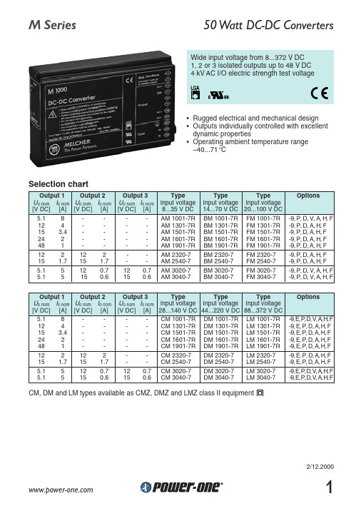
•Rugged electrical and mechanical design •Outputs individually controlled with excellent dynamic properties•Operating ambient temperature range –40...71°CWide input voltage from 8...372 V DC1, 2 or 3 isolated outputs up to 48 V DC 4 kV AC I/O electric strength test voltageSelection chartLGACM, DM and LM types available as CMZ, DMZ and LMZ class II equipment2/12.2000Input voltage 6 wide-input ranges (1:5)refer to selection chartOutputEfficiency U i nom, I o nom up to 83%i nom o nom±0.6% U o nom Output voltage switching noise IEC/EN 61204, total typ. 50 mV ppi min i max o nom o nom Load regulation U i nom, 0...I o nom, each output regulated typ. 0.15% U o nom Minimum load not required0 A Current limitation main output rectangular U/I characteristic typ. 110% I o nomo nom Operation in parallel by current limitation, only main outputsi nom o nomU i nom, I o nom, A/B/C/D/FM with ext. diode in input line up to 7 msProtectionInput reverse polarity built-in fusei min Input overvoltage lockout typ. 110% U i maxOutput no-load, overload and short circuit proofo nom Overtemperature switch-off with auto restart T C typ. 100°CControlOutput voltage adjustment single output types0...110% U o nom Status indication LEDs: OK, inhibit, overloadSafetyApprovals EN 60950, UL 1950, CSA C22.2 No. 950Class of equipment AM, BM, CM, DM, FM, LM class I Protection degree units without options IP 40class I, I/O 4 kV ACO/case 1 kV ACElectrostatic discharge IEC/EN 61000-4-2, level 4 (8/15 kV)criterion B Electromagnetic field IEC/EN 61000-4-3, level x (20 V/m)criterion A/B Electr. fast transients/bursts IEC/EN 61000-4-4, input, level 3/4 (2/4 kV)criterion A/B Surge IEC/EN 61000-4-5, input, level 3/4 (2/4 kV)criterion A Electromagnetic emissions CISPR 22/EN 55022, conducted class BEnvironmentalOperating ambient temperature U i nom, I o nom, convection cooled–25...71°C Operating case temperature C i nom, o nom–25...95°C Storage temperature non operational–40...100°C Damp heat IEC/EN 60068-2-3, 93%, 40°C56 daysn Shock IEC/EN 60068-2-27, 6 ms100 g nn Random vibration IEC/EN 60068-2-64, 20...500 Hz 4.9 g n rms MTBF MIL-HDBK-217E, G B, 40°C, single output types320'000 h OptionsExtended temperature range–40...71°C, ambient, operating-9 Electronic inrush current limitation Eo nomInput and/or output undervoltage monitoring, excludes option V D0...D9 Test sockets for check of output voltage A Enhanced electric strength test 2 kV AC H Fuse not user accessible FPin allocationMechanical data ArrayTolerances ±0.3 mm (0.012") unless otherwise indicated.AccessoriesFront panels 19” (Schroff/Intermas)Mating H11 connectors with screw, solder, fast-on or press-fit terminalsConnector retention facilities and code key system for connector codingFlexible PCB for connecting the converter via an H11 connector, if mounted on a PCB Chassis or wall mounting plates for frontal accessUniversal mounting brackets for chassis or DIN-rail mounting。
M7 VHF数据传输器说明书

The M7 VHF data transceiver is a rugged ½ - 5 wattVHF data radio modem with an RS-232 or optional422/485 serial interface, perfect for SCADA andtelemetry applications. Additional options includeIP65-rated (“weatherproof”) enclosure and/or GPS.Product O verviewLong-Range OperationOperating in the VHF 136-155MHz frequency band (other bands available), the RV-M7-VA radio modem works over 60 miles point-to-point and many miles with omni-directional antennas. All RV-M7 modems support store-and-forward repeating for wide-area coverage.Fast PollingThe M7 transceiver has a 5mS PLL in it, making it one of the fastest telemetry radios available, especially well suited for polled, DNP and MODBUS applications. Its can send up to 50 transmissions per second.High Speed and High EfficiencyThe RV-M7 operates with user-selectable over-the air data rates of 800 to 19200bps. Faster rates for higher efficiency or lower-speed for increased communication range.GPS OptionThe optional internal GPS allows the RV-M7 to be a powerful Automatic Vehicle Locating (AVL) system or Time Space Position Information (TSPI) reporting device.Fully ProgrammableIt is configured with a serial connection using industry-standard AT commands. Parameters such as network IDs, unit ID and transmission rate are easily configured. The M7 is easily configured through the included PC program “Radio Manager”. Digital Base BandData rate, modulation, and IF bandwidth are digitally programmed. Wide (25kHz) and Narrow (12.5kH) IF bandwidths may be user-configured. The over-the-air data rate may be adjusted to suit a particular application.Real-time diagnostics and statisticsChannel performance, RSSI, RF power, packet counters, and radio configuration are easily accessed via the serial port or remotely over-the-air.Very Low Power ConsumptionThe advanced VHF transceiver is integrated with a 32-bit microprocessor-based modem in one easy-to mount package. It has very low power consumption, and sleep modes that allow it to be active and consume a minimum amount of resources.Rugged and “Weatherproof”The RV-M7 is available with optional IP65-rated “weatherproof”connections and enclosure. All models include protection against damage from over-temperature, high VSWR, and reverse voltage.Flexible Addressing and Error CorrectionThe RV-M7 uses a 16 bit address with a 16 bit network mask, allowing for many devices to be co-located without receiving each other, as well as the creation of sophisticated network topologies.For More InformationFor more information about this or any other Raveon product, call in the U.S.A. 1-760-444-5995.RV-M7-V ATechnical Specifications are subject to change without notice.Raveon Technologies Corporation2461 Impala DriveCarlsbad, CA 92010Copyright Raveon Technologies Corp, 2012Phone: +1-760-444-5995All rights reservedFax: +1-760-444-5997Email:****************Version C3. Printed in the USAGeneral SpecificationsModel:RV-M7-Vx-oo (x=band) (oo=options) RV-M7-VM (MURS model) Size: 4.60” X 2.60” X .956 (11.7cm X 6.6cm X 2.43cm) Weight:6 ozInput Voltage: 10 – 16 VDC Current draw:Receiving data: <65mA (55mA typ. at 12VDC)Transmitting data: (1.8A @ 5w, 1.1A @ 2W typical) Frequency Band:Band Frequency A 136-155MHz Available Frequencies: B 150-174MHz SRS-M7-VBMURS 5 MURS chan. SRS-M7-VM Serial Port Baud Rates (programmable)1.2k,2.4k, 4.8k, 9.6k, 19.2k, 38.4k, 57.6k, 115.2k Over-the-air baud rates (programmable) Narrow IF: 800, 1200, 2000, 2400, 4.8k, 5142, 8K, 9.6kWide IF: 1200, 2000, 2400, 4.8k, 8k, 9.6k, 19.2k Operating ModeSimplex or Half-duplex Full Spec Operating Temperature range -30°C to +60°CTX-RX and RX-TX turn-around time <5mS Wake-up time<500mS from OFF <5mS from Sleep Front Panel LEDsPower , Status (Carr Det, TX, mode…) RF I/O ConnectorBNC (Female) Power CableRaveon P/N: RT-CB-H1 AddressingIndividual address: 65,536 Groups: 254Transmitter SpecificationsRF Power Output 500mW – 5.0 W programmable (2W max for MURS model)Maximum Duty Cycle 100% @ 2W to 40C, 25% @5W (100% w/ optional heatsink) Frequency Deviation± 2.2kHz (N) ± 3.3kHz (W)RF BandwidthFull-band without tuning Occupied bandwidth 11 kHz (-N) 16kHz(-W)TX Spurious outputs < -70dBc TX Harmonic outputs < -80dBc Occupied BandwidthPer FCCFCC Emissions Designator 11K0F1D (narrowband mode) 15K0F1D (wideband mode) Frequency Stability Better than ±2.5ppmReceiver SpecificationsRX sensitivity (1% PER, N) ................... 9600bps < -108dBm4800bps < -114dB 1200bps < -118dBRF No-tune bandwidth ......................... Full-band without tuning Adjacent Channel Selectivity ................ -70dB (1200bps Wide) Adjacent Channel Selectivity ................ -65dB (1200bps Narrow) Adjacent Channel Selectivity ................ -60dB (4800bps Narrow) Alternate Channel Selectivity ............... -70dB Blocking and spurious rejection ........... -80dBRX intermodulation rejection ............... -75dB (4800bps Narrow) RX intermodulation rejection ............... -80dB (1200bps Narrow)Interface SpecificationsSerial Interface PortConnector Type DB-9IO Voltage Levels RS-232, RS-485, RS-422(user selectable) Word length7 or 8 bits, N, O, or E Modem handshake signalsRTS, CTS, CDAT Commands OverviewChannel Number, Operating Frequency, IF bandwidth Modem StatisticsPower-savings modesUnit Address and Destination address Network Address Mask ARQ error correction on/off Baud Rate, parity, stop bitsSelect Packet or Streaming mode of data transmission Store-and-forward Repeating configurationHardware flow control operation LEDs operation or disabledFor a complete feature list see the technical manual here:/support.html。
法国尚飞管状电机技术参数

法国尚飞管状电机技术参数
下面将详细介绍法国尚飞管状电机的技术参数:
1.输入电源参数:
2.功率参数:
法国尚飞管状电机的功率参数包括额定功率和峰值功率。
额定功率是指电机在额定负载条件下工作的功率,峰值功率是指电机在短时间内能够承受的最大功率。
不同型号的管状电机具有不同的功率参数,可以根据具体应用需求选择合适的型号。
3.转速参数:
法国尚飞管状电机的转速参数包括空载转速和额定转速。
空载转速是指电机在无载荷情况下的转速,额定转速是指电机在额定负载条件下的转速。
不同型号的管状电机具有不同的转速范围,可以根据具体应用需求选择合适的型号。
4.扭矩参数:
法国尚飞管状电机的扭矩参数包括额定扭矩和峰值扭矩。
额定扭矩是指电机在额定负载条件下的输出扭矩,峰值扭矩是指电机在短时间内能够输出的最大扭矩。
不同型号的管状电机具有不同的扭矩参数,可以根据具体应用需求选择合适的型号。
5.效率参数:
6.控制方式:
法国尚飞管状电机支持多种控制方式,包括开环控制和闭环控制。
开环控制是指电机输出转矩和速度的控制不依赖于反馈信号,闭环控制是指电机输出转矩和速度的控制依赖于反馈信号。
闭环控制可以提高系统的稳定性和精度,常用于对转矩和速度要求较高的应用。
总结:
以上是法国尚飞管状电机的一些主要技术参数,包括输入电源参数、功率参数、转速参数、扭矩参数、效率参数和控制方式。
这些参数可以根据具体的应用需求进行选择和配置,以实现最佳的性能和效果。
法国尚飞管状电机以其先进的技术和优良的性能受到广泛的应用和认可。
RQA0008NXAQS中文资料

RQA0008NXAQSSilicon N-Channel MOS FETREJ03G1569-0100Rev.1.00Jul 04, 2007Features• High Output Power, High Gain, High EfficiencyPout = +36 dBm, Linear Gain = 18 dB, PAE = 65% (f = 520 MHz)• Compact package capable of surface mountingOutline*UPAK is a trademark of Renesas Technology Corp.Absolute Maximum Ratings(Ta = 25°C)UnitRatingsItem SymbolDrain to source voltage V DSS 16 V Gate to source voltage V GSS ±5 V Drain current I D 2.4 A Channel dissipation Pch note 10 W Channel temperature Tch 150 °CStorage temperature Tstg –55 to +150 °CNote: Value at Tc = 25°CThis device is sensitive to electro static discharge. An adequate careful handling procedure is requested.Electrical Characteristics(Ta = 25°C)Item Symbol Min. Typ Max. Unit Test ConditionsZero gate voltage drain current I DSS — — 10 µA V DS = 16 V, V GS = 0 Gate to source leak current I GSS — — ±2 µA V GS = ±5 V, V DS = 0 Gate to source cutoff voltage V GS(off) 0.15 0.4 0.8 V V DS = 6 V, I D = 1 mA Forward Transfer Admittance |yfs| — 2.4 — S V DS = 6 V, I D = 1.2 A Input capacitance Ciss — 44 — pF V GS = 5 V, V DS = 0, f = 1 MHz Output capacitance Coss — 25 — pF V DS = 6 V, V GS = 0, f = 1 MHz Reverse transfer capacitance Crss — 6.0 — pF V DG = 6 V, V GS = 0, f = 1 MHz — 36 — dBm Output Power Pout — 3.98 — WPower Added Efficiency PAE — 65 — % V DS = 6 V, I DQ = 400 mAf = 520 MHz, Pin = +20 dBmMain CharacteristicsEvaluation Circuit (f = 520 MHz)S Parameter(V DS = 6 V, I DQ = 400 mA, Zo = 50 Ω)S11 S21 S12 S22(deg.) MAG ANG(deg.)(deg.)MAG ANGf(MHz) MAG ANG(deg.) MAG ANG100 0.883 -170.0 8.48 84.9 0.021 -3.0 0.867 -175.4 150 0.904 -175.7 5.46 80.1 0.021 -5.3 0.879 -177.3 200 0.902 -178.2 4.13 72.6 0.021 -12.0 0.872 -178.5 250 0.900 179.6 3.30 67.1 0.021 -16.5 0.872 -179.7 300 0.898 177.8 2.75 61.6 0.021 -19.8 0.873 179.5 350 0.898 176.2 2.34 56.2 0.020 -24.2 0.873 178.8 400 0.897 174.8 2.04 50.9 0.020 -27.7 0.874 178.4 450 0.898 173.4 1.80 45.7 0.020 -31.3 0.873 177.8 500 0.899 172.3 1.61 40.7 0.020 -34.4 0.873 177.4 550 0.900 171.2 1.46 35.5 0.019 -38.2 0.875 176.8 600 0.900 170.1 1.33 30.5 0.019 -41.5 0.876 176.5 650 0.899 169.0 1.22 25.5 0.019 -45.0 0.876 176.0 700 0.899 167.9 1.13 20.5 0.019 -47.8 0.878 175.6 750 0.899 166.9 1.04 15.6 0.018 -51.2 0.878 175.2 800 0.898 165.8 0.97 10.6 0.018 -54.8 0.880 174.9 850 0.899 164.7 0.91 5.7 0.018 -57.4 0.878 174.4 900 0.901 163.7 0.85 0.9 0.018 -60.9 0.880 173.9 950 0.903 162.7 0.80 -3.9 0.017 -63.5 0.882 173.5 1000 0.903 161.8 0.75 -8.7 0.017 -66.5 0.883 173.1 1050 0.903 160.8 0.71 -13.4 0.017 -69.3 0.884 172.6 1100 0.905 159.8 0.68 -18.1 0.016 -71.9 0.883 172.1 1150 0.906 158.8 0.64 -22.8 0.016 -74.8 0.886 171.6 1200 0.907 157.8 0.61 -27.3 0.016 -76.8 0.888 171.2 1250 0.909 156.8 0.58 -32.0 0.015 -79.6 0.891 170.8 1300 0.911 155.8 0.55 -36.6 0.015 -81.9 0.893 170.4 1350 0.912 154.9 0.52 -41.2 0.015 -84.1 0.896 170.0 1400 0.912 154.0 0.50 -45.8 0.015 -86.2 0.897 169.5 1450 0.912 153.1 0.48 -50.3 0.014 -88.6 0.898 169.1 1500 0.913 152.1 0.46 -54.8 0.014 -90.2 0.900 168.7 1550 0.914 151.2 0.44 -59.2 0.014 -92.6 0.900 168.4 1600 0.915 150.3 0.42 -63.8 0.014 -94.1 0.902 167.8 1650 0.916 149.4 0.40 -68.3 0.013 -95.9 0.903 167.4 1700 0.915 148.5 0.39 -72.6 0.013 -97.6 0.904 167.0 1750 0.914 147.6 0.38 -76.9 0.013 -99.0 0.904 166.4 1800 0.913 146.7 0.36 -81.1 0.013 -100.8 0.906 165.8 1850 0.915 145.7 0.35 -85.3 0.013 -102.2 0.909 165.5 1900 0.920 144.5 0.34 -89.5 0.013 -103.9 0.909 165.0 1950 0.923 143.3 0.33 -93.6 0.013 -105.8 0.910 164.5 2000 0.925 142.3 0.31 -97.9 0.013 -107.2 0.911 163.9 2050 0.926 141.4 0.30 -102.1 0.013 -108.7 0.913 163.5 2100 0.928 140.5 0.29 -106.3 0.013 -109.9 0.914 163.0 2150 0.929 139.6 0.28 -110.6 0.013 -112.2 0.916 162.4 2200 0.930 138.7 0.27 -114.7 0.013 -112.8 0.917 161.8 2250 0.932 137.8 0.27 -118.9 0.013 -114.9 0.921 161.5 2300 0.931 137.1 0.26 -123.0 0.013 -116.5 0.921 161.0 2350 0.930 136.3 0.25 -127.1 0.013 -118.5 0.921 160.5 2400 0.926 135.5 0.24 -131.2 0.013 -120.2 0.924 159.9 2450 0.922 134.4 0.24 -135.4 0.014 -121.9 0.923 159.5 2500 0.920 133.3 0.23 -139.5 0.014 -123.7 0.921 159.0Package DimensionsOrdering InformationPart Name Quantity Shipping Containerφ178 mm reel, 12 mm emboss tapingRQA0008NXTL-E 1000pcs.Note: For some grades, production may be terminated. Please contact the Renesas sales office to check the state of production before ordering the product.Refer to "/en/network " for the latest and detailed information.Renesas Technology America, Inc.450 Holger Way, San Jose, CA 95134-1368, U.S.A Tel: <1> (408) 382-7500, Fax: <1> (408) 382-7501Renesas Technology Europe LimitedDukes Meadow, Millboard Road, Bourne End, Buckinghamshire, SL8 5FH, U.K.Tel: <44> (1628) 585-100, Fax: <44> (1628) 585-900Renesas Technology (Shanghai) Co., Ltd.Unit 204, 205, AZIACenter, No.1233 Lujiazui Ring Rd, Pudong District, Shanghai, China 200120Tel: <86> (21) 5877-1818, Fax: <86> (21) 6887-7898Renesas Technology Hong Kong Ltd.7th Floor, North Tower, World Finance Centre, Harbour City, 1 Canton Road, Tsimshatsui, Kowloon, Hong Kong Tel: <852> 2265-6688, Fax: <852> 2730-6071Renesas Technology Taiwan Co., Ltd.10th Floor, No.99, Fushing North Road, Taipei, Taiwan Tel: <886> (2) 2715-2888, Fax: <886> (2) 2713-2999Renesas Technology Singapore Pte. Ltd.1 Harbour Front Avenue, #06-10, Keppel Bay Tower, Singapore 098632 Tel: <65> 6213-0200, Fax: <65> 6278-8001Renesas Technology Korea Co., Ltd.Kukje Center Bldg. 18th Fl., 191, 2-ka, Hangang-ro, Yongsan-ku, Seoul 140-702, Korea Tel: <82> (2) 796-3115, Fax: <82> (2) 796-2145Renesas Technology Malaysia Sdn. BhdUnit 906, Block B, Menara Amcorp, Amcorp Trade Centre, No.18, Jalan Persiaran Barat, 46050 Petaling Jaya, Selangor Darul Ehsan, Malaysia Tel: <603> 7955-9390, Fax: <603> 7955-9510RENESAS SALES OFFICES。
VISHAY VLMF31. 数据手册

Vishay SemiconductorsVLMF31..High Intensity SMD LEDFEATURES•SMD LED with exceptional brightness •Luminous intensity categorized•Compatible with automatic placement equipment•EIA and ICE standard package•Compatible with IR Reflow, vapor phase and wave solder processes acc. to CECC 00802 and J-STD-020C•Available in 8 mm tape •Low profile package•Non-diffused lens: excellent for coupling to light pipes and backlighting •Low power consumption •Luminous intensity ratio in one packaging unit I Vmax /I Vmin ≤ 1.6•Lead (Pb)-free device-RoHS compliant •Preconditioning: acc. to JEDEC Level 2a •ESD-withstand voltage:up to 2 kV according to JESD22-A114-B19225DESCRIPTIONThis device has been designed to meet the increasing demand for AlInGaP technology.The package of the VLMF31.. is the PLCC-2.It consists of a lead frame which is embedded in a white thermoplast. The reflector inside this package is filled up with clear epoxy.APPLICATIONS •Automotive: Backlighting in dashboards and switches•Telecommunication: Indicator and backlighting in telephone and fax•Indicator and backlight for audio and video equip-ment•Indicator and backlight in office equipment •Flat backlight for LCDs, switches and symbols •General usePARTS TABLEPARTCOLOR, LUMINOUS INTENSITY ANGLE OF HALF INTENSITY (± ϕ)TECHNOLOGY VLMF31Q2T1-GS08Soft Orange, I V = (90 to 355) mcd 60°AllnGaP on GaAs VLMF31Q2T1-GS18Soft Orange, I V = (90 to 355) mcd 60°AllnGaP on GaAs VLMF31R1S2-GS08Soft Orange, I V = (112 to 280) mcd 60°AllnGaP on GaAs VLMF31R1S2-GS18Soft Orange, I V = (112 to 280) mcd 60°AllnGaP on GaAs VLMF31S1T1-GS08Soft Orange, I V = (180 to 355) mcd 60°AllnGaP on GaAs VLMF31S1T1-GS18Soft Orange, I V = (180 to 355) mcd60°AllnGaP on GaAsVishay Semiconductors VLMF31..Note:1) Tamb = 25°C unless otherwise specified2) Driving the LED in reverse direction is suitable for a short term application Note:1) Tamb = 25°C unless otherwise specified2) in one Packing Unit IVmax/I Vmin≤ 1.6Note:Luminous intensity is tested at a current pulse duration of 25 ms and an accuracy of ± 11 %.The above type numbers represent the order groups which include only a few brightness groups. Only one group will be shipped on each reel (there will be no mixing of two groups on each reel).In order to ensure availability, single brightness groups will not be or-derable.In a similar manner for colors where wavelength groups are mea-sured and binned, single wavelength groups will be shipped on any one reel. In order to ensure availability, single wavelength groups will not be orderable.Note:Wavelengths are tested at a current pulse duration of 25 ms and an accuracy of ± 1 nm.ABSOLUTE MAXIMUM RATINGS1), VLMF31..PARAMETER TEST CONDITION SYMBOL VALUE UNIT Reverse voltage2)V R5V DC Forward current T amb≤ 85°C I F30mA Surge forward current t p≤ 10 µs I FSM0.1A Power dissipation P V80mW Junction temperature T j125°C Operating temperature range T amb- 40 to + 100°C Storage temperature range T stg- 40 to + 100°CThermal resistance junction/ ambient mounted on PC board(pad size > 16 mm2)R thJA400K/WOPTICAL AND ELECTRICAL CHARACTERISTICS1), VLMF31.., SOFT ORANGEPARAMETER TEST CONDITION PART SYMBOL MIN TYP.MAX UNIT Luminous intensity2)I F = 20 mA VLMF31Q2T1I V90355mcdVLMF31R1S2I V112280mcdVLMF31S1T1I V180355mcd Dominant wavelength I F = 20 mAλd598605611nm Peak wavelength I F = 20 mAλp610nm Angle of half intensity I F = 20 mAϕ± 60deg Forward voltage I F = 20 mA V F 2.0 2.6V Reverse voltage I R = 10 µA V R5V Junction capacitance V R = 0, f = 1 MHz C j15pFLUMINOUS INTENSITY CLASSIFICATIONGROUP LIGHT INTENSITY [MCD]STANDARD OPTIONAL MIN MAXP 14556 25671Q 17190 290112R 1112140 2140180S 1180224 2224280T 12803552355450CROSSING TABLEVISHAY OSRAMVLMF31Q2T1LOT676-Q2T1VLMF31R1S2LOT676-R1S2VLMF31S1T1LOT676-S1T1COLOR CLASSIFICATIONGROUP SOFT ORANGEDOM. WAVELENGTH (NM)MIN. MAX.159860126006033602605460460756066096608611Vishay SemiconductorsVLMF31..TYPICAL CHARACTERISTICST amb = 25°C unless otherwise specifiedFigure 1. Forward Current vs. Ambient TemperatureFigure 3. Rel. Luminous Intensity vs. Angular Displacement 05101520253035400102030405060708090100T am b - Am b ient Temperat u re (°C)16615I - F o r w a r d C u r r e n t (m A )F0.40.200.20.40.695 103190.60.90.80°30°10°20°40°50°60°70°80°0.71.0I v r e l -R e l a t i v e L u m i n o u s I n t e n s i t yFigure 4. Relative Intensity vs. WavelengthFigure 5. Forward Current vs. Forward VoltageFigure6. Relative Luminous Intensity vs. Forward Current1101001.01.52.0 2.53.0V F -For w ard V oltage (V )95 10878F I -F o r w a r d C u r r e n t (m A )Vishay SemiconductorsVLMF31..PACKAGE DIMENSIONS IN MMFigure7. Rel. Luminous Intensity vs. Ambient Temperature Figure8. Forward Voltage vs. Ambient TemperatureVishay SemiconductorsVLMF31..METHOD OF TAPING/POLARITY AND TAPE AND REEL SMD LED (VLM3 - SERIES)Vishay’s LEDs in SMD packages are available in an antistatic 8 mm blister tape (in accordance with DIN IEC 40 (CO) 564) for automatic component inser-tion. The blister tape is a plastic strip with impressed component cavities, covered by a top tape.TAPING OF VLM.3..REEL PACKAGE DIMENSION IN MM FOR SMD LEDS, TAPE OPTION GS08(= 1500 PCS.)REEL PACKAGE DIMENSION IN MM FOR SMD LEDS, TAPE OPTION GS18(= 8000 PCS.) PREFEREDFigure9. Tape dimensions in mm for PLCC-2Figure 10. Reel dimensions - GS08Figure 11. Reel dimensions - GS18Vishay SemiconductorsVLMF31..SOLDERING PROFILEBARCODE-PRODUCT-LABEL EXAMPLE:A)Type of component B)Manufacturing PlantC)SEL - Selection Code (Bin):e.g.: Q2 = Code for Luminous Intensity Group 1 = Code for Color Group D)Date Code year/weekE)Day Code (e.g. 3: Wednesday)F)Batch No.G)Total quantity H)Company CodeFigure 12. Vishay Leadfree Reflow Soldering Profile(acc. to J-STD-020C)Figure 13. Double wave soldering of opto devices (all packages)V ISHAYAHBC D E F GVishay SemiconductorsVLMF31..DRY PACKINGThe reel is packed in an anti-humidity bag to protect the devices from absorbing moisture during transpor-tation and storage.FINAL PACKINGThe sealed reel is packed into a cardboard box. A sec-ondary cardboard box is used for shipping purposes.RECOMMENDED METHOD OF STORAGEDry box storage is recommended as soon as the alu-minium bag has been opened to prevent moisture absorption. The following conditions should be observed, if dry boxes are not available:• Storage temperature 10°C to 30°C • Storage humidity ≤ 60 % RH max.After more than 672 hours under these conditions moisture content will be too high for reflow soldering.In case of moisture absorption, the devices will recover to the former condition by drying under the following condition:192 hours at 40°C + 5°C/ - 0°C and < 5 % RH (dry air/nitrogen) or96 hours at 60°C + 5°C and < 5 % RH for all device containers or24 hours at 100°C + 5°C not suitable for reel or tubes.An EIA JEDEC Standard JESD22-A112 Level 2a label is included on all dry bags.Example of JESD22-A112 Level 2a labelESD PRECAUTIONProper storage and handling procedures should be fol-lowed to prevent ESD damage to the devices espe-cially when they are removed from the Antistatic Shielding Bag. Electro-Static Sensitive Devices warn-ing labels are on the packaging.VISHAY SEMICONDUCTORS STANDARD BAR-CODE LABELSThe Vishay Semiconductors standard bar-code labels are printed at final packing areas. The labels are on each packing unit and contain Vishay Semiconductors specific data.VLMF31..Vishay SemiconductorsOZONE DEPLETING SUBSTANCES POLICY STATEMENTIt is the policy of Vishay Semiconductor GmbH to1.Meet all present and future national and international statutory requirements.2.Regularly and continuously improve the performance of our products, processes, distribution and operatingsystems with respect to their impact on the health and safety of our employees and the public, as well as their impact on the environment.It is particular concern to control or eliminate releases of those substances into the atmosphere which are known as ozone depleting substances (ODSs).The Montreal Protocol (1987) and its London Amendments (1990) intend to severely restrict the use of ODSs and forbid their use within the next ten years. Various national and international initiatives are pressing for an earlier ban on these substances.Vishay Semiconductor GmbH has been able to use its policy of continuous improvements to eliminate the use of ODSs listed in the following documents.1.Annex A, B and list of transitional substances of the Montreal Protocol and the London Amendments respectively2.Class I and II ozone depleting substances in the Clean Air Act Amendments of 1990 by the EnvironmentalProtection Agency (EPA) in the USA3.Council Decision 88/540/EEC and 91/690/EEC Annex A, B and C (transitional substances) respectively. Vishay Semiconductor G mbH can certify that our semiconductors are not manufactured with ozone depleting substances and do not contain such substances.We reserve the right to make changes to improve technical designand may do so without further notice.Parameters can vary in different applications. All operating parameters must be validated for each customer application by the customer. Should the buyer use Vishay Semiconductors products for any unintended or unauthorized application, the buyer shall indemnify Vishay Semiconductors against all claims, costs, damages, and expenses, arising out of, directly or indirectly, any claim of personal damage, injury or deathassociated with such unintended or unauthorized use.Vishay Semiconductor GmbH, P.O.B. 3535, D-74025 Heilbronn, GermanyLegal Disclaimer NoticeVishayNoticeSpecifications of the products displayed herein are subject to change without notice. Vishay Intertechnology, Inc., or anyone on its behalf, assumes no responsibility or liability for any errors or inaccuracies.Information contained herein is intended to provide a product description only. No license, express or implied, by estoppel or otherwise, to any intellectual property rights is granted by this document. Except as provided in Vishay's terms and conditions of sale for such products, Vishay assumes no liability whatsoever, and disclaims any express or implied warranty, relating to sale and/or use of Vishay products including liability or warranties relating to fitness for a particular purpose, merchantability, or infringement of any patent, copyright, or other intellectual property right. The products shown herein are not designed for use in medical, life-saving, or life-sustaining applications. Customers using or selling these products for use in such applications do so at their own risk and agree to fully indemnify Vishay for any damages resulting from such improper use or sale.。
MICROMEGA 高精度过程控制器说明书

CN77000 R300和R500控制器,图片中含RHS-43孔锯, 易于钻圆孔。
有关订购信息, 请参见最后一页。
CN77333-A2 NEMA 12款方形开孔。
CN77533 NEMA 4方形开孔。
图片为实际尺寸。
1⁄16 DIN MICROMEGA ®自动调谐PID温度/过程控制器U 高精度:±0.5°C (0.9°F), 读数的0.03% U品质优秀, 还有5年保修支持 U 通用输入—过程电压/电流、热电偶、RTD U 双4位数字LED 显示屏和指示器, 用于显示输出和报警状态 U 可选RS232或RS485, OMEGA ® 协议U 继电器、SSR 、DC 脉冲、0 ~ 10 V, 以及 0 ~ 20 mA 输出类型 U 斜坡到设定值功能 U 通用电源, 90 ~ 250 Vac 或Vdc U 双输出和双报警功能U 隔离模拟输出或远程设定值可选将方形控制器放置于圆孔中!高精度、高品质MICROMEGA ®控制器在过程控制中提供无与伦比的灵活性。
每台设备均允许用户从10个热电偶类型(J 、K 、T 、E 、R 、S 、B 、C 、N 和JDIN )、Pt RTD (100、500或1000 Ω, 385或392曲线)或者模拟电压或电流输入中选择输入类型。
电压/电流输入可完全扩展到各工程单位,可选择小数点,是压力、流量或其他过程输入的理想之选。
MICROMEGA ®控制器具有大型双LED 显示屏,采用前面板配置,可选温度/过程输入,并接受90 ~ 250 Vac 或Vdc 通用电源。
提供单和双输入配置,CN77000系列适用于继电器、SSR 、DC 脉冲或模拟电压或电流输出。
单报警是标准配置。
可选项包括第二报警、 RS232、RS485、模拟输出以及远程设定值可选。
“300”系列控制器有许多特色,更大,紧凑型1⁄4 DIN 控制器,1⁄16 DIN 尺寸。