ADV7127
BPS4000产品规格说明书

at BPS4000 rev(yy/mm/dd)SupersedingDoc160-006AM040322BHTI Alternate Materials List M&P 299-947-100-690115BHTI Procurement Specification for Epoxy Adhesive, Heat Resistant M&P 299-947-320-820507BHTI Adhesive Film and Primer System, Intermediate CureTemperature (260-290º F) Service Temperature 67-225º F)M&P 68A900000G011101BAC Finish Spec: F-15M&P 74A900000E990308BAC Finish Specification for F18 Aircraft M&P 74A900004DG M051220BAC Ctrl: Fract Crit Parts, F-18M&P 74A901001F981208BAC Std Finish Codes: F-18 A\C M&P 901-947-002CA D950510BHTI Finish Specification for the V-22 Aircraft (Bell Boeing) Model901) EMD AircraftM&P A-A-208See Special Notes DL C120719FED Ink, Marking, Stencil, Opaque Use A-A-00208 in lieu of A-A-208.M&P A-A-2962Cancelled - no s/s spec A980810Cancel Notice 2FED Commercial Item Description Enamel, Alkyd, Exterior, SolventBased, Low VocOk to use canc spec.M&P A-A-3097DC-970506Notice 4FED Commercial Item Description Adhesives, Cyanoacrylate, RapidRoom Temperature-Curing, SolventlessM&P A-A-3165DE A071116FED Lacquer, Gloss, for A/C Use M&P A-A-00208See Special Notes DL D121001FED Commercial Item Description Ink, Marking, Stencil, Opaque(Porous and Non-Porous Surfaces)Use A-A-00208 in lieu of A-A-208.M&P A-A-52080B980523Notice 1FED Tape, Lacing, and Tying, Nylon M&P A-A-52081DF B980523Notice 1FED Tape, Lacing, and Tying, Polyester M&P A-A-52082DC D090817FED Tape, Lacing and Tying, TFE-Fluorocarbon M&P A-A-52083BJ C040223FED Tape, Lacing, and Tying, Glass M&P A-A-52084B980523Notice 1FED Tape, Lacing and Tying, Aramid M&P A-A-55829DC A110322DLA Acetic Acid, Glacial, Technical M&P A-A-56032CN D030521Notice 1FED Commercial Item Description (CIDS) Ink, Marking, Epoxy Base M&P A-A-59126-970926FED Terminals, Feedthru (Insulated) and Terminals, Stud (Insulatedand Noninsulated)ENG A-A-59132CR A100607Validation Notice 1DLA Amyl Acetate, Technical M&P A-A-59135CR-971028FED Commercial Item Description Packaging Material, Sheet M&P A-A-59136CR-971028FED Cushioning Material, Packaging, Closed Cell Foam Plank M&PA-A-59178DD A041012Notice 1USGOVT Nipple, Electrical Terminal ENGA-A-59503DC C110303FED Commercial Item Description Nitrogen, Technical M&PA-A-59551CP A091022USGOVT Wire, Electrical, Copper (Uninsulated) M&PA-A-59569DJ C090122Notice 1DLA Qualification Sampling and Testing of Steels for TransverseTensile PropertiesENG A-A-59588DJ B120130Notice 1FED Commercial Item Description Rubber, Silicone M&P A-A-59877CT-100909FED Commercial Item Description Insulating Compound, Electrical,EmbeddingM&P AIR4127CG - 071101SAE Steel: Chemical Composition and Hardenability M&P AISI-1010Unavailable-AISI Low Carb Stl Unavailable M&P AISI-50100Unavailable-AISI Bearing Stl Unavailable M&P AISI-52100Unavailable-AISI Bearing Stl Unavailable M&P AISI-B-1112Unavailable-AISI Low Carb Free Mach Stl Unavailable M&P AISI-C-1212Unavailable-AISI Material Spec, Stl Unavailable M&P AISI-C-1213Unavailable-AISI Low Carb Free Mach Stl Unavailable M&P AISI-C-1214Unavailable-AISI Material Spec, Stl Unavailable M&P AMS 2175CR A100601SAE Castings, Classification and Inspection of M&P AMS 2201Cancelled CN Can940901SAE Tolerances Aluminum and Aluminum Alloy Bar, Rod, Wire, andForging Stock Rolled or Cold-FinishedANSI H35.2M&P AMS 2221G060201SAE Tolerances, Copper and Copper Alloy Bars and Rods M&P AMS 2222BG J060201SAE Tolerances, Copper and Copper Alloy Sheet, Strip, and Plate M&Pat BPS4000 rev(yy/mm/dd)SupersedingDocAMS 2223BF H060201SAE Tolerances Copper and Copper Alloy Seamless Tubing M&P AMS 2224G060201SAE Tolerances Copper and Copper Alloy Wire M&P AMS 2241CN R070701SAE Tolerances, Corrosion and Heat-Resistant Steel, Iron Alloy,M&PTitanium, and Titanium Alloy Bars and WireM&P AMS 2242CC G080604SAE Tolerances Corrosion and Heat Resistant Steel, Iron Alloy,Titanium and Titanium Alloy Sheet, Strip and PlateAMS 2243DH K130601SAE Tolerances Corrosion and Heat-Resistant Steel Tubing M&PM&P AMS 2248DB G110301SAE Chemical Check Analysis Limits Corrosion and Heat-ResistantSteels and Alloys, Maraging and other Highly-Alloyed Steels,and Iron AlloysAMS 2249CN G090701SAE Chemical Check Analysis Limits Titanium and Titanium Alloys M&PM&P AMS 2259CN E071201SAE Chemical Check Analysis Limits Wrought Low-Alloy andCarbon SteelsAMS 2269CN F060501SAE Chemical Check Analysis Limits Nickel, Nickel Alloys, andM&PCobalt AlloysM&P AMS 2300CU L100801SAE Steel Cleanliness, Premium Aircraft-Quality Magnetic ParticleInspection ProcedureM&P AMS 2301CT K100801SAE Steel Cleanliness, Aircraft Quality Magnetic Particle InspectionProcedureAMS 2303CT F100801SAE Steel Cleanliness, Aircraft Quality, Martensitic CorrosionM&PResistant Steels Magnetic Particle Inspection ProcedureM&P AMS 2304CV B100801SAE Steel Cleanliness, Special Aircraft-Quality Magnetic ParticleInspection ProcedureM&P AMS 2310BE F060201SAE Qualification Sampling and Testing of Steels for TransverseTensile PropertiesAMS 2315DF G130201SAE Determination of Delta Ferrite Content M&P AMS 2350Cancelled - no s/s spec CN BA891001SAE Standards and Test Methods Ok to use canc spec.M&PM&P AMS 2355DB K110301SAE Quality Assurance Sampling and Testing Aluminum Alloys andMagnesium Alloy Wrought Products (Except Forging Stock),and Rolled, Forged, or Flash Welding RingsAMS 2360CN D070701SAE Room Temperature Tensile Properties of Castings M&PM&P AMS 2370DB K110601SAE Quality Assurance Sampling and Testing Carbon and Low-AlloySteel Wrought Products and Forging StockAMS 2371DB J110601SAE Quality Assurance Sampling and Testing Corrosion and Heat-M&PResistant Steels and Alloys Wrought Products and ForgingStockM&P AMS 2372DB F110601SAE Quality Assurance Sampling and Testing Carbon and Low-AlloySteel ForgingsAMS 2375CN D070601SAE Control of Forgings Requiring First Article Approval M&P AMS 2380CN F080601SAE Approval and Control of Premium-Quality Titanium Alloys M&P AMS 2400DG X130201SAE Plating, Cadmium M&P AMS 2401DF J130201SAE Plating, Cadmium Low Hydrogen Content Deposit M&P AMS 2403BM L041001SAE Plating, Nickel General Purpose M&P AMS 2404CH F081201SAE Plating, Electroless Nickel M&P AMS 2405DL E131001SAE Electroless Nickel Plate, Low Phosphorous M&P AMS 2406DE M121101SAE Plating, Chromium Hard Deposit M&P AMS 2408DL K130901SAE Plating, Tin M&P AMS 2410CR K100401SAE Plating, Silver Nickel Strike, High Bake M&P AMS 2411DM H131201SAE Plating, Silver for High Temperature Applications M&P AMS 2412CN J091201SAE Plating, Silver Copper Strike, Low Bake M&P AMS 2416CU L101201SAE Plating, Nickel-Cadmium Diffused M&P AMS 2417DL J130901SAE Plating, Zinc-Nickel Alloy M&P AMS 2418CU H110201SAE Plating, Copper M&P AMS 2419BM C030501SAE Plating, Cadmium-Titanium M&PM&P AMS 2420D021201SAE Plating of Aluminum for Solderability Zinc Immersion Pre-Treatment Processat BPS4000 rev(yy/mm/dd)SupersedingDocAMS 2423See Special Notes CE D020401SAE Plating, Nickel Hard Deposit Continue to use AMS-QQ-N-290 for Class 2Nickel.M&P AMS 2424CR F100401SAE NI Plate, Low Stressed Deposit M&P AMS 2426DL E130901SAE Coating, Cadmium Vacuum Deposition M&P AMS 2427DD D070701SAE Aluminum Coating Ion Vapor Deposition M&P AMS 2429CY D111001SAE Bronze Plate Masking M&P AMS 2430DB S120701SAE Shot Peening, Automatic M&P AMS 2432DF D130201SAE Shot Peening, Computer Monitored M&P AMS 2433C041001SAE Plating, Nickel-Thallium-Boron or Nickel-Boron M&P AMS 2434CY D110901SAE Plating, Tin-Zinc Alloy M&P AMS 2435Noncurrent CN G070601SAE Coating, Tungsten Carbide-Cobalt Coating, Detonation Process M&P AMS 2437BN C710111SAE Coating, Plasma Spray Deposition M&P AMS 2438CL D090701SAE Plating, Chromium Thin, Hard, Dense Deposit M&P AMS 2444BM A001201SAE Coating, Titanium Nitride Physical Vapor Deposition M&P AMS 2451CW C110701SAE Plating, Brush General Requirements M&PAMS 2460See Special Notes DF A130301SAE Plating, Chromium If dwg requires chrome plate per AMS-QQ-C-320then stress relief and embritlmnt (emb) bake reliefper BPS4620. If dwg req's chrome plate per AMS2460then stress relief and bake relief per AMS M&PAMS 2468Cancelled CN G981001SAE Hard Anodic Coating Treatment of Aluminum Alloys AMS 2469M&P AMS 2469DM J140201SAE Hard Anodic Coating Treatment of Aluminum and AluminumAlloys Processing and Performance RequirementsM&P AMS 2470DH N130701SAE Anodic Treatment of Aluminum Alloys Chromic Acid Process M&P AMS 2471DM H140201SAE Anodic Treatment of Aluminum Alloys Sulfuric Acid Process,Undyed CoatingM&P AMS 2472DD F070801SAE Anodic Treatment of Aluminum Alloys Sulfuric Acid Process,Dyed CoatingM&P AMS 2473DK H130801SAE Chemical Film Treatment for Aluminum Alloys General PurposeCoatingM&P AMS 2474Noncurrent DD D060201SAE Chemical Treatment for Aluminum Alloys Low ElectricalResistance CoatingAMS 2477M&P AMS 2477DD A100401SAE Conversion Coating for Aluminum Alloys Low Electrical Coating M&P AMS 2481CP J100201SAE Phosphate Treatment Antichafing M&P AMS 2482CN D100101SAE Hard Anodic Coating on Aluminum AlloysPolytetrafluoroethylene (PTFE)-Impregnated or CodepositedM&P AMS 2485BY K080101SAE Coating, Black Oxide M&P AMS 2486CR E100501SAE Conversion Coating of Titanium Alloys Fluoride-PhosphateTypeM&P AMS 2487CN A000301SAE Anodic Treatment of Titanium and Titanium Alloys Solution pH12.4 MaximumM&P AMS 2488D000606SAE Anodic Tr: Ti, Ti Alys M&P AMS 2515DE G130101SAE Polytetrafluoroethylene (PTFE) Resin Coating Low Build, 370 to400 °C (698 to 752 °F) FusionM&P AMS 2516DF E130301SAE Polytetrafluoroethylene (PTFE) Resin Coating High Build, 370to 400 °C (698 to 752 °F) FusionM&P AMS 2525DJ D130701SAE Graphite Coating, Thin Lubricating Film Impingement Applied M&P AMS 2526DE D130101SAE Molybdenum Disulfide Coating, Thin Lubricating FilmImpingement AppliedM&P AMS 2590DD-101201SAE Rotary Flap Peening of Metal Parts M&P AMS 2615BM F060901SAE Pressure Testing Hydraulic Pressure as Specified M&P AMS 2630CR C100101SAE Inspection, Ultrasonic Product Over 0.5 Inch (12.7 mm) Thick M&P AMS 2631CW D110701SAE Ultrasonic Inspection Titanium and Titanium Alloy Bar and Billet M&P AMS 2632BN A950301SAE Inspection, Ultrasonic, of Thin Materials 0.50 Inch (12.7 mm)and Under in Cross-Sectional ThicknessM&P AMS 2635Cancelled Can810701SAE Radiographic Insp ASTM E1742M&Pat BPS4000 rev(yy/mm/dd)SupersedingDocAMS 2640Cancelled CH Can960401SAE Magnetic Particle Inspection ASTM E1444M&P AMS 2645Cancelled CH Can950201SAE Fluorescent Penetrant Inspection ASTM E1417M&P AMS 2649DM D131201SAE Etch Inspection of High Strength Steel Parts M&P AMS 2658CN C091001SAE Hardness and Conductivity Inspection of Wrought AluminumAlloy PartsM&P AMS 2664CH F950701SAE Brazing, Silver for Use Up to 800 °F (427 °C)M&P AMS 2665DH H130501SAE Brazing, Silver for Use up to 400 °F (204 °C)M&P AMS 2666Cancelled Can840101SAE Ag Braz, High Temp AMS 2664M&P AMS 2670BK J060601SAE Brazing, Copper M&P AMS 2671Cancelled CH Can920101SAE Copper Brazing Corrosion and Heat Resistant Steels andAlloysAMS 2670M&P AMS 2672CY G120101SAE Brazing, Aluminum Torch or Furnace M&P AMS 2673DB E120101SAE Brazing, Aluminum and Aluminum Alloys Molten Flux (Dip)M&P AMS 2675DF H130201SAE Brazing, Nickel Alloy Filler Metal M&P AMS 2680C010601SAE Electron-Beam Welding for Fatigue Critical Applications M&P AMS 2681B000301SAE Electron Beam Welding M&P AMS 2685Noncurrent CP E071001SAE Welding, Tungsten Arc, Inert Gas GTAW Method M&P AMS 2689Noncurrent CH A980201SAE Fusion Welding Titanium and Titanium Alloys M&P AMS 2694DE C130101SAE In-Process Welding of Castings M&P AMS 2700DA E111101SAE Passivation of Corrosion Resistant Steels All acceptance testing shall be per Class 4except for Martensitic CRES alloy 440C,which requires no class testing.M&PAMS 2728DC C120901SAE Heat Treatment of Wrought Copper Beryllium Alloy Parts M&P AMS 2745CJ A071201SAE Induction Hardening of Steel Parts M&P AMS 2750DB E120701SAE Pyrometry M&P AMS 2753CF C080801SAE Liquid Salt Bath Ferritic Nitrocarburizing Non-Cyanide Bath M&P AMS 2755Cancelled CM Can090701SAE Nitriding, Molten Salt Bath Process not available, consider AMS 2753 asreplacement.M&P AMS 2759CE E081001SAE Heat Treatment of Steel Parts General Requirements M&PAMS 2759/1CJ E090201SAE Heat Treatment of Carbon and Low-Alloy Steel Parts MinimumTensile Strength Below 220 ksi (1517 MPa)Supersedes MIL-H-6875 for carbon & low-alloy steels below 220 ksi.M&PAMS 2759/2CR F100501SAE Heat Treatment of Low-Alloy Steel Parts Minimum TensileStrength 220 ksi (1517 MPa) and Higher Supersedes MIL-H-6875 for low-alloy steels,220 ksi & higher.M&PAMS 2759/3CE E080801SAE Heat Treatment Precipitation-Hardening Corrosion-Resistantand Maraging Steel Parts Supersedes MIL-H-6875 for precipitationhardening & maraging steel.M&PAMS 2759/4CA C080301SAE Heat Treatment Austenitic Corrosion-Resistant Steel Parts Supersedes MIL-H-6875 for austentic steels.M&P AMS 2759/5D040601SAE Heat Treatment Martensitic Corrosion Resistant Steel Parts Supersedes MIL-H-6875 for martensiticsteels.M&P AMS 2759/6BM B051101SAE Gas Nitriding and Heat Treatment of Low - Alloy Steel Parts Use Standard Drawing Notes per BDS2240.M&P AMS 2759/7CT B100501SAE Carburizing and Heat Treatment of Carburizing Grade SteelPartsM&PAMS 2759/8CG A070601See Special Notes SAE Ion Nitriding 1. Infrared pyrometry may be used to measuretemperature. 2. The nitriding temperature may beless than 50 degrees below the tempering or agingtemperature provided that the core hardness is notreduced. 3. for small loads, a minimum of twot t ti i b d i li M&PAMS 2759/9CL D090501SAE Hydrogen Embrittlement Relief (Baking of Steel Parts)Supersedes MIL-H-6875 for stress relievingsteels.M&P AMS 2759/10CN A060601SAE Automated Gaseous Nitriding Controlled by Nitriding Potential M&P AMS 2759/11BW-050401SAE Stress Relief of Steel Parts M&P AMS 2762Noncurrent CP B020101SAE Carburizing Carbon and Low-Alloy Steel Parts M&P AMS 2768CR C100701SAE Heat Treatment of Magnesium Alloy Castings M&P AMS 2769DD B091201SAE Heat Treatment of Parts in a Vacuum M&P AMS 2770DM L140501SAE Heat Treatment of Wrought Aluminum Alloy Parts M&Pat BPS4000 rev(yy/mm/dd)SupersedingDocAMS 2771DF E130201SAE Heat Treatment of Aluminum Alloy Castings M&P AMS 2772CW F110701SAE Heat Treatment of Aluminum Alloy Raw Materials M&P AMS 2774DC D121001SAE Heat Treatment Wrought Nickel Alloy and Cobalt Alloy Parts M&P AMS 2800CN D060801SAE Identification Finished Parts M&P AMS 2801B030301SAE Heat Treatment of Titanium Alloy Parts M&PM&P AMS 2807CF B080201SAE Identification Carbon and Low-Alloy Steels, Corrosion and Heat-Resistant Steels and Alloys Sheet, Strip, Plate and AircraftTubingAMS 3025CN C090901SAE Polyalkylene Glycol Heat Treat Quenchant M&P AMS 3106Cancelled Can830401SAE Primer, Adhesive, Corr Inhib AMS 3107M&P AMS 3107A910401SAE Primer, Adhesive, Corr-Inhibiting M&P AMS 3195CV F110501SAE Silicone Rubber Sponge, Closed Cell, Medium M&PM&P AMS 3216G050901SAE Fluorocarbon (FKM) Rubber High-Temperature - FluidResistant Low Compression Set 70 to 80AMS 3218C050901SAE Fluorocarbon (FKM) Rubber High-Temperature - FluidM&PResistant Low Compression Set 85 to 95M&P AMS 3276CB E080301SAE Sealing Compound, Integral Fuel Tanks and General Purpose,Intermittent Use to 360 °F (182 °C)AMS 3301DB H110601SAE Silicone Rubber, General Purpose, 40 Durometer M&P AMS 3305H900401SAE Silicone Rubber, Gen Purp, 75-85M&P AMS 3374DL D131101SAE Sealing Compound Aircraft Firewall, Silicone M&P AMS 3410J981001SAE Flux, Ag Braz M&P AMS 3411D981001SAE Flux Silver Brz, High Temp M&PM&P AMS 3644BL G060901SAE Plastic: Polyimide for Molded Rod, Bar, and Tube, Plaque, andformed PartsM&P AMS 3645CY D120101SAE Polychlorotrifluoroethylene (PCTFE), Compression MoldedHeavy Sections, UnplasticizedM&P AMS 3650CY D120101SAE Rods, Sheets, and Molded Shapes, Polychlorotrifluoroethylene(PCTFE) UnplasticizedAMS 3651Cancelled Can870401SAE PTFE AMS 3667M&P AMS 3651Cancelled Can870401PTFE AMS 3652M&P AMS 3651Cancelled Can870401PTFE AMS 3656M&P AMS 3651Cancelled Can870401PTFE AMS 3660M&P AMS 3652C930101SAE PTFE Film, Non-Crit Grade M&P AMS 3656CW H110801SAE PTFE Extrusions, Normal Strength, As Sintered M&P AMS 3657CW F110801SAE PTFE, Extrusions, Premium Strength, As Sintered M&P AMS 3658CW F110801SAE PTFE, Extrusions, Premium M&P AMS 3659CW F110801SAE Polytetrafluoroethylene (PTFE) Extrusions, Premium Strength,M&PSintered and Stress-RelievedAMS 3660CW E110801SAE Polytetrafluoroethylene Moldings M&P AMS 3666DB E120101SAE PTFE Sht, Glass Reinforced M&PM&P AMS 3667CW E110801SAE Polytetrafluoroethylene Sheet, Molded General Purpose Grade,As SinteredAMS 3668CW E110801SAE PTFE, Moldings, Premium Grade, A Sintered M&P AMS 3670/1B950401SAE Unfilled Polyamide-Imide, Bar M&P AMS 3824CN C950901SAE Cloth, Glass Finished for Resin Laminates M&P AMS 4001Cancelled CK Can070701SAE Aluminum Sheet and Plate 0.12Cu (1100-0) Annealed ASTM B209M&P AMS 4013DM G140201SAE Aluminum Sheet, Laminated Surface Bonded M&PM&P AMS 4015CN L070201SAE Aluminum Alloy, Sheet and Plate 2.5Mg - 0.25Cr (5052-0)AnnealedM&P AMS 4016DE M130101SAE Aluminum Alloy, Sheet and Plate 2.5Mg - 0.25Cr (5052-H32)Strain Hardened, Quarter Hard, and Stabilizedat BPS4000 rev(yy/mm/dd)SupersedingDocAMS 4017CN K041201SAE Aluminum Alloy Sheet and Plate 2.5Mg - 0.25Cr (5052-H34)M&PStrain-Hardened, Half Hard, and StabilizedM&P AMS 4023Noncurrent CN E840401SAE Aluminum Alloy Sheet and Plate Alclad 1.0Mg - 0.60Si - 0.28Cu- 0.20Cr (Alclad 6061; -T6 Sheet, -T651 Plate)AMS 4025CE L080701SAE Aluminum Alloy, Sheet and Plate 1.0Mg - 0.60Si-0.28Cu-AMS-QQ-A-250/11A - cancelled - 2008M&P0.20Cr(6061-0) AnnealedAMS-QQ-A-250/11A - cancelled - 2008M&P AMS 4026CE M080701SAE Aluminum Alloy, Sheet and Plate 1.0Mg -0.60Si-0.28Cu-0.20Cr(6061;-T4 Sheet, T-451 Plate) Solution Heat Treated andNaturally AgedAMS-QQ-A-250/11A - cancelled - 2008M&P AMS 4027CE N080701SAE Aluminum Alloy, Sheet and Plate 1.0Mg -0.60Si-0.28Cu-0.20Cr(6061;-T6 Sheet, T-651 Plate) Solution and Precipitation HeatTreatM&P AMS 4037CY P111201SAE Aluminum Alloy, Sheet and Plate 4.4Cu - 1.5Mg - 0.60Mn(2024; - T3 Flat Sheet, T351 Plate) Solution Heat TreatedM&P AMS 4048CW N100801SAE Aluminum Alloy Sheet and Plate, Alclad 5.6Zn - 2.5Mg - 1.6Cu -0.23Cr (Alclad 7075-O) Annealed or When Specified, "Asfabricated" (Alclad 7075-F)AMS 4049CW L101201SAE Aluminum Alloy Sheet and Plate, Alclad 5.6Zn - 2.5Mg - 1.6Cu -M&P0.23Cr (Alclad 7075; -T6 Sheet - T651 Plate) Solution andPrecipitation Heat TreatedAMS 4056DB G101001SAE Aluminum Alloy, Sheet and Plate 4.4Mg - 0.70Mn - 0.15CrM&P(5083-01)M&P AMS 4080CN N091201SAE Aluminum Alloy, Drawn Seamless Tubing 1.0Mg - 0.60Si -0.28Cu - 0.20Cr (6061-O) AnnealedM&P AMS 4081CC J080601SAE Aluminum Alloy Tubing, Hydraulic, Seamless, Drawn, Round1.0Mg - 0.60Si - 0.28Cu - 0.20Cr (6061-T4) Solution HeatTreated and Naturally AgedM&P AMS 4083DE L121101SAE Aluminum Alloy Tubing, Hydraulic, Seamless, Drawn, Round1.0Mg - 0.60Si - 0.28Cu - 0.20Cr- (6061-T6) Solution andPrecipitation Heat TreatedM&P AMS 4086BL N060901SAE Aluminum Alloy, Drawn, Round, Seamless Hydraulic Tubing4.4Cu-1.5Mg-0.60Mn (2024-T3) Solution Heat Treated, ColdWorked, and Naturally AgedAMS 4088BT K070301SAE Aluminum Alloy, Drawn, Seamless Tubing 4.4Cu-1.5Mg-M&P0.60Mn (2024-T3) Solution Heat Treated and Cold WorkedAMS 4107F051101SAE Alum Aly Die Forg, (7050-T14)M&PM&P AMS 4113CH E030701SAE Aluminum Alloy, Extruded Profiles 1.0Mg - 0.60Si - 0.28Cu -0.20Cr (6061-T6) Solution and Precipitation Heat TreatedM&P AMS 4115CU H090701SAE Aluminum Alloy, Rolled or Cold-Finished, Bars, Rods, Wire,and Flash Welded Rings Annealed 1.0Mg - 0.60Si - 0.2Cu -0.20Cr (6061-0)M&P AMS 4116CN H090701SAE Aluminum Alloy, Bars, Rods, and Wire 1.0Mg - 0.60Si - 0.3Cu -0.20Cr (6061-T4) Cold Finished, Solution Heat Treated andNaturally AgedM&P AMS 4117CM J090701SAE Aluminum Alloy, Rolled or Cold Finished Bars, Rods, and Wireand Flash Welded Rings 1.0Mg -0.60Si - 0.28Cu - 0.20Cr(6061; - T6, -T651) Solution and Precipitation Heat TreatedAMS 4120M&P AMS 4119Cancelled CN Can900101SAE Aluminum Alloy Bars, Rolled, Drawn, or Cold Finished 4.4Cu -1.5Mg - 0.60Mn (2024-T351) Stress Relief StretchedAMS 4120R020901SAE Aluminum Alloy, Rolled or Cold Finished Bars, Rods, and WireM&P4.4Cu - 1.5 Mg - 0.60Mn (2024) Solution Heat Treated andNaturally Aged (T4) Solution Heat Treated, Cold Worked, andNaturally Aged (T351)M&P AMS 4121CA H071101SAE Aluminum Alloy Bars, Rods, and Wire, Rolled or Cold Finished4.5Cu - 0.85Si - 0.80Mn - 0.50Mg (2014-T6) Solution andPrecipitation Heat TreatedM&P AMS 4123CN H060101SAE Aluminum Alloy, Rolled or Cold Finished Bars and Rods (7075-T651) Solution and Precipitation Heat TreatedM&P AMS 4124DG E120901SAE Aluminum Alloy, Rolled or Cold Finished Bars, Rods, and Wire5.6Zn-2.5Mg-1.6Cu-0.23Cr (7075-T7351) Solution HeatTreated, Stress Relieved by Stretching and OveragedM&P AMS 4128CN D071001SAE Aluminum Alloy Bars, Rolled or Cold Finished 1.0Mg - 0.60Si -0.30Cu - 0.20Cr (6061-T451) Solution Heat Treated and StressRelieved by Stretchingat BPS4000 rev(yy/mm/dd)SupersedingDocAMS 4132DF G130201SAE Aluminum Alloy, Die and Hand Forgings, Rolled Rings, andM&PForging Stock 2.3Cu-1.6Mg-1.1Fe-1.0Ni-0.18Si-0.07Ti (2618-T61) Solution and Precipitation Heat TreatedM&P AMS 4133CN E090301SAE Aluminum Alloy Forgings and Rolled Rings 4.4Cu -0.85Si -0.80Mn - 0.50Mg (2014-T6) Solution and Precipitation HeatTreatedAMS 4133M&P AMS 4135Cancelled CN Can860401SAE Aluminum Alloy Forgings 4.5Cu - 0.85Si - 0.80Mn - 0.50Mg(2014-T6) Solution and Precipitation Heat TreatedAMS 4141CE F081001SAE Aluminum Alloy Die Forgings 5.6Zn - 2.5Mg - 1.6Cu - 0.23CrM&P(7075-T73) Solution and Precipitation Heat TreatedAMS 4144BN F060501SAE Aluminum Alloy, Hand Forgings and Rolled Rings 6.3Cu -M&P0.30Mn - 0.18Zr - 0.10V - 0.06Ti (2219-T852/T851) SolutionHeat Treated, Mechanically Stress Relieved, and PrecipitationHeat-TreatedM&P AMS 4149D020901SAE Aluminum Alloy, Die and Hand Forgings 5.6n - 2.5Mg - 1.6Cu -0.23Cr (7175-T74) Solution and Precipitation Heat TreatedAMS 4150DG M130401SAE Aluminum Alloy, Extrusions and Rings 1.0Mg - 0.60Si - 0.28Cu -M&P0.20Cr - (6061-T6) Solution and Precipitation Heat TreatedM&P AMS 4162D030701SAE Aluminum Alloy, Extrusions 6.3Cu - 0.30Mn - 0.18Zr - 0.10V -0.06Ti (2219-T8511) Solution Treated, Stress Relief Stretched,Straightened, and Precipitation Heat TreatedM&P AMS 4173DG F130401SAE Aluminum Alloy, Extrusions 1.0Mg - 0.60Si - 0.30Cu - 0.20Cr(6061-T6511) Solution Heat Treated, Stress Relieved byStretching, Straightened, and Precipitation Heat TreatedM&P AMS 4181C030401SAE Aluminum Alloy, Welding Wire 7.0Si - 0.38Mg - 0.10Ti (4008)(UNS A94008)M&P AMS 4182CN G091201SAE Alum Aly Wire, Annealed 5.0Mg - 0.12Mn - 0.12Cr (5056-0)AnnealedAMS 4185DB E120201SAE Fill Mtl, Alum Braz, 12SI, (4047)M&P AMS 4188Cancelled Can861001SAE Wldg Wire AMS 4181M&P AMS 4188Cancelled Can861001SAE Wldg Wire AMS 4233M&P AMS 4188Cancelled Can861001SAE Wldg Wire AMS 4244M&P AMS 4188Cancelled Can861001SAE Wldg Wire AMS 4245M&P AMS 4188Cancelled Can861001SAE Wldg Wire AMS 4246M&PM&P AMS 4210CN K050301SAE Aluminum Alloy, Castings 5.0Si - 1.2Cu - 0.50Mg (355.0-T51)Precipitation Heat TreatedM&P AMS 4212CU K110201SAE Aluminum Alloy Castings 5.0Si - 1.2Cu - 0.50Mg (355.0-T6)Solution and Precipitation Heat TreatedM&P AMS 4214CN J080601SAE Castings, Aluminum Alloy Sand 5.0Si - 1.2Cu - 0.50Mg (355.0T71) Solution Heat Treated and OveragedM&P AMS 4215CN H080301SAE Aluminum Alloy, Castings 5.0Si - 1.2Cu - 0.50Mg (C355.0-T6)Solution and Precipitation Heat TreatedM&P AMS 4217CN H070401SAE Aluminum Alloy, Castings 7.0Si - 0.32Mg (A356.0-T6) (formerlyT6P Temper) Solution and Precipitation Heat TreatedM&P AMS 4218CN J100101SAE Aluminum Alloy Castings 7.0Si-0.35Mg (A356.0-T6) (formerlyT6P Temper) Solution and Precipitation Heat TreatedM&P AMS 4223CN D070401SAE Aluminum Alloy, Castings 4.5Cu - 0.70Ag - 0.30Mn - 0.25Mg -0.25Ti (A201.0-T4) Solution Heat Treated and Naturally AgedOk to use canc spec.M&P AMS 4224Cancelled - no s/s spec CN C100101SAE Aluminum Alloy Castings, Sand 4.0Cu - 2.1Ni - 2.0Mg - 0.30Cr -0.30Mn - 0.13T - 0.13V (243.0) StabilizedM&P AMS 4225CN D070601SAE Aluminum Alloy, Heat Resistant, Castings 5.0Cu - 1.5Ni -0.25Mn - 0.25Sb - 0.25Co - 0.20Ti - 0.20Zr (203.0-T6) SolutionHeat Treated and Precipitation Heat TreatedM&P AMS 4226Noncurrent CN A830101SAE Aluminum Alloy Castings, High Strength 5.0Cu - 0.35Mn -0.18Zr- 0.10V (224.0) Solution and Precipitation Heat Treated(Overaged)AMS 4227Cancelled - no s/s spec CN E050701SAE Aluminum Alloy, Casting, Sand, 8.0Cu 6.0Mg 0.50Mn 0.50Ni,Ok to use canc spec.M&PAs CastAMS 4229DA F120201SAE Aluminum Alloy Castings, High Strength 4.5Cu - 0.7Ag -M&P0.30Mn - 0.25Mg - 0.25Ti (A201.0-T7) Solution Heat Treatedand OveragedM&P AMS 4233C030301SAE Aluminum Alloy, Welding Wire 4.5 Cu - 0.70Ag - 0.30Mn -0.25Mg - 0.25Ti (A201.0-T7) Solution Heat Treated andOveragedat BPS4000 rev(yy/mm/dd)SupersedingDocAMS 4235CN B080301SAE Aluminum Alloy Castings 4.6Cu - 0.35Mn - 0.25Mg - 0.22Ti(A206.0-T71) Solution and Precipitation Heat TreatedM&P AMS 4236DF C130201SAE Aluminum Alloy Castings 4.6Cu - 0.35Mn - 0.25Mg - 0.22Ti(A206.0-T4) Solution Heat Treated and Naturally AgedM&P AMS 4237Cancelled - no s/s spec CN B070401SAE Aluminum Alloy Castings, Sand 4.6Cu - 0.35Mn - 0.25Mg -0.22Ti (206.0 - T71) Solution Heat Treated and Naturally AgedOk to use canc spec.M&P AMS 4241CN D091101SAE Aluminum Alloy Castings 7.0Si - 0.58Mg - 0.15Ti -0.06Be(D357.0 - T6) Solution and Precipitation Heat Treated DendriteArm Spacing (DAS) ControlledM&PAMS 4244CE B080701SAE Aluminum Alloy, Welding Wire 4.6Cu - 0.35Mn - 0.25Mg -0.22Ti for Welding A206.0 Type AlloysM&PAMS 4245CR E100401SAE Aluminum Alloy, Welding Wire 5.0Si - 1.2Cu - 0.50Mg (355)(UNS A03550)M&PAMS 4246Noncurrent CP D080201SAE Aluminum Alloy, Welding Wire 7.0Si - 0.52Mg (357) (UNSA03570)M&PAMS 4260Not Acceptable to Use atParker HannifinAerospace CL G080601SAE Alum Aly Cast, Invest (356.0-T6)BPS4829AMS 4260 rev. G unacceptable for ParkerUse. BPS4829 created as replacement.M&PAMS 4261CN F091201SAE Aluminum Alloy Castings, Investment 7.0Si - 0.32Mg (356.0 -T51) Precipitation Heat TreatedM&P AMS 4280CN J080601SAE Aluminum Alloy Castings, Permanent Mold 5.0Si - 1.2Cu -0.5Mg (355.0-T71) Solution Heat Treated and OveragedM&P AMS 4284DC J110301SAE Aluminum Alloy Castings, Permanent Mold 7.0Si - 0.30Mg(356.0-T6) Solution and Precipitation Heat TreatedM&P AMS 4289CN-011101SAE Aluminum Alloy Castings 7.0Si - 0.55Mg - 0.12Ti (F357.0-T6)Solution and Precipitation Heat TreatedM&P AMS 4291CT H101001SAE Aluminum Alloy, Die Castings 8.5Si - 3.5Cu (A380.0-F) (SeeAS1990) As CastM&P AMS 4315CK-050701SAE Aluminum Alloy Sheet and Plate 5.6Zn - 2.5Mg - 1.6Cu - 0.23Cr7075: (-T76 Sheet, -T7651 Plate) Solution and PrecipitationHeat TreatedM&PAMS 4316CY A111101SAE Aluminum Alloy, Alclad Sheet and Plate 5.6Zn - 2.5Mg M&P AMS 4437DM F140201SAE Magnesium Alloy Castings, Sand 8.7Al - 0.70Zn (AZ91C-T6)Solution Heat Treated and AgedM&P AMS 4507BW H011101SAE Copper Alloy (Brass), Sheet, Strip, and Plate 70Cu - 30Zn HalfHard (H02)M&P AMS 4510CN G010501SAE Phosphor Bronze, Sheet, Strip, and Plate 94.5Cu - 4.0Sn -0.19P Spring Temper (H08)M&P AMS 4511A040701SAE Copper Beryllium Alloy Castings 97Cu-2.1Be-0.52(Co+Ni)-0.28Si Solution and Precipitation Heat Treated (TFOO)M&P AMS 4530CY J110901SAE Copper-Beryllium Alloy Sheet, Strip, and Plate 98Cu - 1.9BeSolution Heat Treated (TB00)M&P AMS 4533DF D130201SAE Copper-Beryllium Alloy, Bars and Rods 98Cu - 1.9Be Solutionand Precipitation Heat Treated (TF00, formerly AT)-UNSC17200M&PAMS 4597CY A111201SAE Copper-Nickel-Tin Alloy, Bars and Rods 77Cu - 15Ni - 8SnSolution Annealed, Cold Finished and Spinodal Hardened (TXTS)M&PAMS 4631Noncurrent CL E880401SAE Aluminum Bronze Rods, Bars, and Forgings 90.5Cu - 7.5Al -1.95: Stress RelievedM&P AMS 4633CL A031201SAE Bronze, Aluminum Silicon, Rods, Bars, and Forgings 90Cu -7.0Al - 1.8Si Drawn and Stress Relieved (HR50)M&P AMS 4634CL B090301SAE Aluminum Bronze Bars, Rods, and Forgings 905Cu - 7.5Al -1.9Si Stress RelievedM&P AMS 4635CL F090701SAE Aluminum Bronze Bars, Rods, and Forgings 87Cu - 9Al - 3FeStress RelievedM&P AMS 4640CV H110501SAE Aluminum Bronze, Bars, Rods, Shapes, Tubes, and Forgings81.5Cu - 10.0Al - 4.8Ni - 3.0Fe Drawn and Stress Relieved(HR50) or Temper Annealed (TQ50)M&PAMS 4650DF M130201SAE Copper-Beryllium Alloy, Bars, Rods, Shapes and Forgings98Cu - 1.9Be Solution Heat Treated TB00 (A)M&P AMS 4651CN C050701SAE Copper-Beryllium Alloy, Bars and Rods 98Cu - 1.9Be (CDA172) Hard Temper (TD04)M&P AMS 4674CN G060901SAE Nickel - Copper Alloy, Corrosion-Resistant, Bars and Forgings67Ni - 30Cu - 0.04S Free MachiningM&P AMS 4701CN G091001SAE Copper Wire, Oxygen-Free 99.95 (Cu+Ag) Annealed M&P。
ADI CN-0282:USB供电的DVI HDMI至VGA转换器(HDMI2VGA) 使用手册说明
ADI 中文版数据手册是英文版数据手册的译文,敬请谅解翻译中可能存在的语言组织或翻译错误,ADI 不对翻译中存在的差异或由此产生的错误负责。
如需确认任何词语的准确性,请参考ADI 提供的最新英文版数据手册。
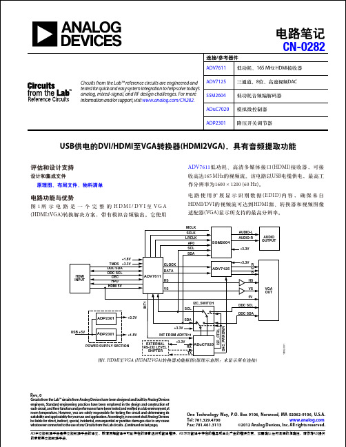
CN-0282Circuits from the Lab™ reference circuits are engineered and tested for quick and easy system integration to help solve today’s analog, mixed-signal, and RF design challenges. For more information and/or support, visit /CN282.ADV7611低功耗、165 MHz HDMI 接收器 ADV7125 三通道、8位、高速视频DACSSM2604 低功耗音频编解码器ADuC7020 模拟微控制器ADP2301降压开关调节器USB 供电的DVI/HDMI 至VGA 转换器(HDMI2VGA),具有音频提取功能Rev. 0Circuits from the Lab™ circuits from Analog Devices have been designed and built by Analog Devicesengineers. Standard engineering practices have been employed in the design and construction of each circuit, and their function and performance have been tested and veri ed in a lab environment at room temperature. However , you are solely responsible for testing the circuit and determining its suitability and applicability for your use and application. Accordingly , in no event shall Analog Devices be liable for direct, indirect, special, incidental, consequential or punitive damages due to any cause whatsoever connected to the use of any Circuits from the Lab circuits. (Continued on last page)One Technology Way, P.O. Box 9106, Norwood, MA 02062-9106, U.S.A. Tel: 781.329.4700 Fax: 781.461.3113©2012 Analog Devices, Inc. All rights reserved. HDMI INPUTTMDS DDC SDA DDC SCL CEC ADV7611CLOCK DATAHS VSADV7125R VGA OUTDDC SDADDC SCL ADuC7020SDASCLSSM2604MCLK SCLK LRCLK AP0AUDIO-L AUDIO OUTPUTAUDIO-RHPD I2C_SWITCH G BHS VS HDMI 5V5VSCL SDAI 2C _C T R LD A C _P W R D W NI N T 1INT FROM ADV7611EXTERNAL RS-232 LEVEL SHIFTERRX TXADP2301ADP2301USB +5VPOWER SUPPLY SECTION+1.8V+3.3V +3.3V+1.8V +3.3V+3.3V+3.3V+3.3V10892-001图1. HDMI 至VGA (HDMI2VGA)转换器功能框图(原理示意图:未显示所有连接)电路笔记连接/参考器件评估和设计支持设计和集成文件原理图、布局文件、物料清单电路功能与优势图1所示电路是一个完整的H D M I /D V I 至V G A (HDMI2VGA)转换解决方案,带有模拟音频输出。
2015英国国际防务展(DSEI 2015)的新装备
2015英国国际防务展(DSEI 2015)的新装备作者:陈友龙来源:《坦克装甲车辆》 2015年第23期陈友龙英国国际防务展历来被誉为全世界军工制造业最重要的盛会,也是各国展示军事实力的最好平台。
2015年9月15~18日,在英国伦敦举行的英国国际防务展(DSEI2015)上,来自世界各地的参展商展示了最新研制的设备和系统。
通过展会,我们可以直观地了解世界坦克装甲车辆发展的最新动态。
英国下一代“阿贾克斯”步兵战车据《简氏防务周刊》报道,英国陆军新一代步兵战车“Scout SV”已经被重新命名为“阿贾克斯”(“Ajax”)步兵战车,首辆原型车在此次展会上正式亮相。
“阿贾克斯”步兵战车是通用动力公司此前为西班牙和奥地利军队研制的“ASCOD” (“阿斯科德”)步兵战车的改进型,它打败了英国BAE公司的改进型CV90步兵战车,从而成为英国“未来快速奏效系统”专用车族(FRES-SV)。
英国陆军在2014年9月与通用动力公司签订了一份价值54亿美元的合同以订购589辆“阿贾克斯”系列装甲车,其中245辆为装备了CTAInternational(CTA国际公司)的CT-40 40毫米埋头弹系统的步兵战车,该新型火炮将搭载于洛克希德·马丁英国分公司生产的炮塔之上。
首批三个型号的“阿贾克斯”系列装甲车(包括装甲运兵车和指挥车)计划于2016年交付完毕。
“阿贾克斯”步兵战车乘员为3+8配置,包括驾驶员、车长、炮长和8名全副武装的步兵。
车体采用动力舱前置布局,驾驶员位于车体前部左侧,配有3个显示屏,可显示由16台摄像机采集到的车外120度的视场。
发动机位于驾驶员陈友龙英国国际防务展历来被誉为全世界军工制造业最重要的盛会,也是各国展示军事实力的最好平台。
2015年9月15~18日,在英国伦敦举行的英国国际防务展(DSEI2015)上,来自世界各地的参展商展示了最新研制的设备和系统。
通过展会,我们可以直观地了解世界坦克装甲车辆发展的最新动态。
Motorola 3.5 kHz 产品说明书
RVN4126 3.59100-386-9100-386/T DEVICERVN41772-CD2-3.5MCS/MTSRVN41821-CD2-3.5XTS3000/SABER PORTABLE YES RKN4046KHVN9085 3.51-20 R NO HLN9359 PROG. STAND RVN4057 3.532 X 8 CODEPLUG NO3080385B23 & 5880385B30 MDVN4965 3.59100-WS/T CONFIG KITRVN4053 3.5ASTRO DIGITAL INTERFACE NO3080385B23RVN41842-CD RKN4046A (Portable) 2-3.5ASTRO PORTABLE /MOBILE YES3080369B73 or0180300B10 (Mobile) RVN41831-CD3080369B732-3.5ASTRO SPECTRA MOBILE YES(Low / Mid Power)0180300B10 (High Power) RVN4185CD ASTRO SPECTRA PLUS MOBILE NO MANY OPTIONS; SEESERVICE BRIEF#SB-MO-0101RVN4186CD ASTRO SPECTRA PLUS MANY OPTIONS;MOBILE/PORTABLE COMB SEE SERVICE BRIEF#SB-MO-0101RVN4154 3.5ASTROTAC 3000 COMPAR.3080385B23RVN5003 3.5ASTROTAC COMPARATORS NO3080399E31 Adpt.5880385B34RVN4083 3.5BSC II NO FKN5836ARVN4171 3.5C200RVN4029 3.5CENTRACOM SERIES II NO VARIOUS-SEE MANUAL6881121E49RVN4112 3.5COMMAND PLUS NORVN4149 3.5COMTEGRA YES3082056X02HVN6053CD CT250, 450, 450LS YES AAPMKN4004RVN4079 3.5DESKTRAC CONVENTIONAL YES3080070N01RVN4093 3.5DESKTRAC TRUNKED YES3080070N01RVN4091 3.5DGT 9000 DESKSET YES0180358A22RVN4114 3.5GLOBAL POSITIONING SYS.NO RKN4021AHVN8177 3.5GM/GR300/GR500/GR400M10/M120/130YES3080070N01RVN4159 3.5GP60 SERIES YES PMLN4074AHVN9128 3.5GP300 & GP350RVN4152 3.5GP350 AVSRVN4150 3.5GTX YES HKN9857 (Portable)3080070N01(Mobile) HVN9025CD HT CDM/MTX/EX SERIES YES AARKN4083/AARKN4081RiblessAARKN4075RIBLESS NON-USA RKN4074RVN4098H 3.5HT1000/JT1000-VISAR YES3080371E46(VISAR CONV)RVN4151 3.5HT1000 AVSRVN4098 3.5HT1000/ VISAR CONV’L.YES RKN4035B (HT1000) HVN9084 3.5i750YES HLN-9102ARVN4156 3.5LCS/LTS 2000YES HKN9857(Portable)3080070N01(Mobile) RVN4087 3.5LORAN C LOC. RECV’R.NO RKN4021ARVN4135 3.5M100/M200,M110,M400,R100 includesHVN9173,9177,9646,9774YES3080070N01RVN4023 3.5MARATRAC YES3080070N01RVN4019 3.5MAXTRAC CONVENTIONAL YES3080070N01RVN4139 3.5MAXTRAC LS YES3080070N01RVN4043 3.5MAXTRAC TRK DUPLEX YES3080070N01RVN4178CD MC SERIES, MC2000/2500DDN6124AW/DB25 CONNECTORDDN6367AW/DB9 CONNECTOR RVN41751-CD Rib to MIC connector 1-3.5MCS2000 RKN4062BRVN41131-3.5MCS2000RVN4011 3.5MCX1000YES3000056M01RVN4063 3.5MCX1000 MARINE YES3000056M01RVN4117 3.5MDC/RDLAP DEVICESRVN4105 3.5MOBILE PROG. TOOLRVN4119 3.5MOBITEX DEVICESRVN4128 3.5MPT1327-1200 SERIES YES SEE MANUALRVN4025 3.5MSF5000/PURC/ANALOG YES0180355A30RVN4077 3.5MSF5000/10000FLD YES0180355A30RVN4017K 3.5MT 1000YES RTK4205CRVN4148 3.5MTR 2000YES3082056X02RVN4140 3.5MTRI 2000NORVN41761-CD MTS2000, MT2000*, MTX8000, MTX90001-3.5*programmed by DOS which is included in the RVN4176RVN4131 3.5MTVA CODE PLUG FIXRVN4142 3.5MTVA DOCTOR YES3080070N01RVN4131 3.5MTVA3.EXERVN4013 3.5MTX800 & MTX800S YES RTK4205CRVN4097 1-CD MTX8000/MTX9000,MTS2000,MT2000*,* programmed by DOS which is included in the RVN4176HVN9067CD MTX850/MTX8250MTX950,MTX925RVN4138 3.5MTX-LS YES RKN4035DRVN4035 3.5MX 1000YES RTK4203CRVN4073 3.5MX 800YES RKN4006BHVN9395 P100, P200 LB, P50+, P210, P500, PR3000RVN4134 3.5P100 (HVN9175)P200 LB (HVN9794)P50+ (HVN9395)P210 (HVN9763)P500 (HVN9941)PR3000 (HVN9586)YES RTK4205HVN9852 3.5P110YES HKN9755A/REX1143 HVN9262 3.5P200 UHF/VHF YES RTK4205RVN4129 3.5PDT220YVN4051 3.5PORTABLE REPEATER Portable rptr.P1820/P1821AXRVN4061C 3.5PP 1000/500NO3080385B23 & 5880385B30 RVN5002 3.5QUANTAR/QUANTRO NO3O80369E31RVN4135 3.5R100 (HVN9177)M100/M200/M110/M400YES0180358A52RVN4146 3.5RPM500/660RVN4002 3.5SABER YES RTK4203CRVN4131 3.5SETTLET.EXEHVN9007 3.5SM50 & SM120YESRVN4039 3.5SMART STATUS YES FKN5825AHVN9054 3.5SOFTWARE R03.2 P1225YES3080070N01HVN9001 3.5SOFTWARE R05.00.00 1225LS YES HLN9359AHVN9012 3.5SP50RVN4001N 3.5SPECTRA YES3080369B73 (STANDARD)0180300B10 (HIGH POWER) RVN4099 3.5SPECTRA RAILROAD YES3080369B73RVN4110 3.5STATION ACCESS MODULE NO3080369E31RVN4089A 3.5STX TRANSIT YES0180357A54RVN4051 3.5SYSTEMS SABER YES RTK4203BRVN4075 3.5T5600/T5620 SERIES NO3080385B23HVN9060CD TC3000, TS3000, TR3000RVN4123 3.5VISAR PRIVACY PLUS YES3080371E46FVN4333 3.5VRM 100 TOOLBOX FKN4486A CABLE &ADAPTORRVN4133 3.5VRM 500/600/650/850NORVN4181CD XTS 2500/5000 PORTABLES RKN4105A/RKN4106A RVN41002- 3.5XTS3000 ASTRO PORTABLE/MOBILERVN4170 3.5XTS3500YES RKN4035DRIB SET UPRLN4008E RADIO INTERFACE BOX (RIB)0180357A57RIB AC POWER PACK 120V0180358A56RIB AC POWER PACK 220V3080369B71IBM TO RIB CABLE (25 PIN) (USE WITH XT & PS2)3080369B72IBM TO RIB CABLE (9 PIN)RLN443825 PIN (F) TO 9 PIN (M) ADAPTOR (USE W/3080369B72 FOR AT APPLICATION) 5880385B308 PIN MODULAR TO 25 PIN ”D” ADAPTOR (FOR T5600 ONLY)0180359A29DUPLEX ADAPTOR (MOSTAR/TRAXAR TRNK’D ONLY)Item Disk Radio RIB Cable Number Size Product Required Number Item Disk Radio RIB Cable Number Size Product Required NumberUtilizing your personal computer, Radio Service Software (RSS)/Customer Programming Software (CPS)/CustomerConfiguration Software (CCS) enables you to add or reprogram features/parameters as your requirements change. RSS/CPS/CCS is compatible with IBM XT, AT, PS/2 models 30, 50, 60 and 80.Requires 640K RAM. DOS 3.1 or later. Consult the RSS users guide for the computer configuration and DOS requirements. (ForHT1000, MT/MTS2000, MTX838/8000/9000, Visar and some newer products —IBM model 386, 4 MEG RAM and DOS 5.0 or higher are recommended.) A Radio Interface Box (RIB) may be required as well as the appropriate cables. The RIB and cables must be ordered separately.Licensing:A license is required before a software (RVN) order is placed. The software license is site specific (customer number and ultimate destination tag). All sites/locations must purchase their own software.Be sure to place subsequent orders using the original customer number and ship-to-tag or other licensed sites; ordering software without a licensed customer number and ultimate tag may result in unnecessary delays. To obtain a no charge license agreement kit, order RPX4719. To place an order in the U.S. call 1-800-422-4210. Outside the U.S., FAX 847-576-3023.Subscription Program:The purchase of Radio ServiceSoftware/Customer Programming/Customer ConfigurationSoftware (RVN & HVN kits) entitles the buyer/subscriber to three years of free upgrades. At the end of these three years, the sub-scriber must purchase the same Radio Service Software kit to receive an additional three years of free upgrades. If the sub-scriber does not elect to purchase the same Radio Service Software kit, no upgrades will be sent. Annually a subscription status report is mailed to inform subscribers of the RSS/CPS/CCS items on our database and their expiration dates.Notes:1)A subscription service is offered on “RVN”-Radio Service Software/Customer Programming/Customer Configuration Software kits only.2)“RVN” software must only be procured through Radio Products and Services Division (RPSD). Software not procured through the RPSD will not be recorded on the subscription database; upgrades will not be mailed.3)Upgrades are mailed to the original buyer (customer number & ultimate tag).4)SP software is available through the radio product groups.The Motorola General Radio Service Software Agreement is now available on Motorola Online. If you need assistance please feel free to submit a “Contact Us” or call 800-422-4210.SMART RIB SET UPRLN1015D SMART RIB0180302E27 AC POWER PACK 120V 2580373E86 AC POWER PACK 220V3080390B49SMARTRIB CABLE (9 PIN (F) TO 9 PIN (M) (USE WITH AT)3080390B48SMARTRIB CABLE (25 PIN (F) TO 9 PIN (M) (USE WITH XT)RLN4488ASMART RIB BATTERY PACKWIRELESS DATA GROUP PRODUTS SOFTWARERVN4126 3.59100-386/9100T DEVICES MDVN4965 3.59100-WS/T CONFIG’TN RVN41173.5MDC/RDLAP DEVICESPAGING PRODUCTS MANUALS6881011B54 3.5ADVISOR6881029B90 3.5ADVISOR ELITE 6881023B20 3.5ADVISOR GOLD 6881020B35 3.5ADVISOR PRO FLX 6881032B30 3.5BR8506881032B30 3.5LS3506881032B30 3.5LS5506881032B30 3.5LS7506881033B10 3.5LS9506881035B20 3.5MINITOR III8262947A15 3.5PAGEWRITER 20008262947A15 3.5PAGEWRITER 2000X 6881028B10 3.5TALKABOUT T3406881029B35 3.5TIMEPORT P7308262947A15 3.5TIMEPORT P930NLN3548BUNIVERSAL INTERFACE KITItem Disk Radio NumberSize Product。
波音系列飞机介绍及总体参数
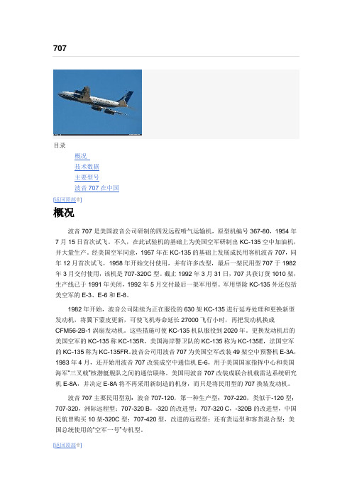
707目录概况技术数据主要型号波音707在中国[返回顶部]概况波音707是美国波音公司研制的四发远程喷气运输机,原型机编号367-80,1954年7月15日首次试飞。
不久,在此试验机的基础上为美国空军研制出KC-135空中加油机,并大量生产。
经美国空军同意,1957年在KC-135的基础上发展成民用客机波音707,同年12月首次试飞,1958年开始交付使用,并有许多改型,最后一架民用型707于1982年3月交付使用,该机是707-320C型。
截止1992年3月31日,707共获订货1010架,生产线已于1991年关闭,1992年5月交付最后一架军用型。
军用型除KC-135外还包括美空军的E-3、E-6和E-8。
1982年开始,波音公司陆续为正在服役的630架KC-135进行延寿处理和更换新型发动机,将翼下蒙皮更新,可使飞机寿命延长27000飞行小时,再把发动机换成CFM56-2B-1涡扇发动机。
这些措施可使KC-135机队服役到2020年。
更换发动机后的美国空军的KC-135称KC-135R,美国海岸警卫队的KC-135称为KC-135E,法国空军的KC-135称为KC-135FR。
波音公司用波音707为美国空军改装49架空中预警机E-3A,1983年4月,还开始用波音707改装成空中通信机E-6,用于美国国家指挥中心和美国海军“三叉戟”核潜艇舰队之间的通信联络。
美国用波音707改装成联合机载雷达系统研究机E-8A,并决定E-8A将不再采用新制造的机身,而只是将民用型的707换装发动机。
波音707主要民用型别:波音707-120,第一种生产型;707-220,类似于-120型;707-320,洲际远程型;707-320 B,-320的改进型;707-320 C,-320B的改进型,中国民航曾购买10架-320C型;707-420型,改进的远程型;还有货运型和客货混合型;美国总统使用的“空军一号”专机型。
adv7127kru140用法

adv7127kru140用法adv7127kru140用法简介adv7127kru140是一款高性能的视频数字-模拟转换器芯片,可用于图像和视频处理应用。
它支持多种输入和输出格式,并提供了丰富的配置选项。
用法一:选择输入格式•支持的输入格式有:RGB、YCrCb、YUV和YPbPr。
•用户可以通过设置相关寄存器来选择所需的输入格式。
•例如,将寄存器INP_SEL的值设置为0x01,即可选择RGB输入格式。
用法二:配置输出格式•adv7127kru140支持多种输出格式,如模拟CVBS、YPbPr和RGB。
•用户可以根据需要选择合适的输出格式,并通过相关寄存器进行配置。
•例如,将寄存器OUTP_FMT的值设置为0x02,即可选择YPbPr输出格式。
用法三:设置输出电平范围•adv7127kru140可以通过寄存器进行输出电平范围的设置。
•用户可以选择合适的范围以适应不同的使用环境。
•例如,将寄存器OUTP_ELV的值设置为0x01,即可选择1V范围的输出电平。
用法四:调整图像亮度、对比度等参数•adv7127kru140内置了图像处理功能,可实现对图像亮度、对比度等参数的调整。
•通过设置相关寄存器,用户可以根据实际需要对图像进行优化。
•例如,将寄存器CONTRAST的值设置为0x80,即可将对比度设置为中等水平。
用法五:降低功耗•adv7127kru140提供了多种功耗管理功能,可帮助用户降低系统功耗。
•例如,可以通过设置寄存器PD_DACS的值为0x01,将数模转换器的功耗降低到最低。
总结adv7127kru140是一款功能强大的视频数字-模拟转换器芯片,可应用于各种图像和视频处理场景。
通过选择合适的输入格式、配置输出格式、调整图像参数和降低功耗等用法,用户可以根据实际需求灵活使用该芯片。
用法六:配置时钟和同步信号•adv7127kru140需要外部提供时钟和同步信号以确保正常工作。
•用户可以根据实际需求,选择合适的时钟频率和同步信号类型,并通过相关寄存器进行配置。
Vaisala WMT700系列风速传感器用户指南说明书
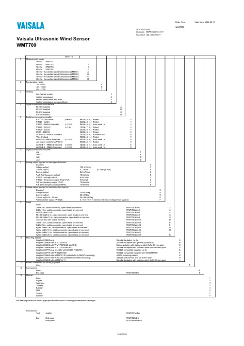
Order Form Valid from2022-02-11MASTERDOC221319-WChecked: AMPN / 2021-12-17Accepted: JGL / 2022-02-11Vaisala Ultrasonic Wind SensorWMT700WMT 7 01Measurement range40 m/s WMT701165 m/s WMT702275 m/s WMT703390 m/s WMT704440 m/s + Accredited Wind Calibration (WMT701)A65 m/s + Accredited Wind Calibration (WMT702)B75 m/s + Accredited Wind Calibration (WMT703)C90 m/s + Accredited Wind Calibration (WMT704)D2Temperature range-10...+60 C A-40...+60 C B-55...+70 C C3HeatingNon-heated version1Heated transducers2Heated transducers and arms3Heated transducers, arms and body44Digital communication interfaceRS-485 isolated ARS-422 isolated BRS-232 isolated CSDI-12 isolated D5Digital communication profileWMT70 - poll mode (default)9600b, 8, N, 1 Polled0WS425 - ASCII 2400b, 8, N, 1 Polled1WS425 - NMEA Extended(v 0183)9600b, 8, N, 1 Auto send 1/s2WS425 - SDI-12 (v 1.3)1200b, 7, E, 1 Polled3WS425 - ASOS 2400b, 8, N, 1 Polled4ROSA - MES12 9600b, 8, N, 1 Polled5US AWOS - NMEA Standard2400b, 8, N, 1 Autosend 5/s6FAA - Federal9600b, 8, N, 1 Polled7AWS520 - NMEA Extended(v 0183)4800b, 8, N, 1 Auto send 1/s8Low power mode for AWS3109600b, 8, N, 1 Polled9MARINE 1 - NMEA Extended(v 0183)4800b, 8, N, 1 Auto send 1/s AMARINE 2 - NMEA Standard(v 0183)4800b, 8, N, 1 Auto send 1/s B6Digital communication unitsm/s Aknots Bmph Ckm/h D7Analog output signals for wind speed channelDisabled0Voltage output100 mV/m/s1Current output 4...20 mA(0...Range m/s)3Current output0.2 mA/m/s4Push-Pull frequency output10 Hz/m/s6WS425 - voltage output8 mV/mph7WS425 - frequency output (Push-Pull) 5 Hz/mph8Pull up frequency output (PNP)10 Hz/m/s APull down frequency output (NPN)10 Hz/m/s B8Analog output signals for wind direction channelDisabled0Voltage output20 mV/Deg ACurrent output50 uA/Deg DCurrent output 4...20 mA44.444 uA/Deg EPotentiometer output (WS425)0...Vref (Vref = external reference voltage from system)F9CableNone1Cable 2 m, cable connector, open leads on one end WMT70Cable12Cable 10 m, cable connector, open leads on one end WMT70Cable23MAWS cable 10 m WMT70Cable34RS485 Cable 2 m, cable connector, open leads on one end WMT70Cable88RS485 Cable 10 m, cable connector, open leads on one end WMT70Cable99Junction Box with Cable 2meters WMT70Cable12DCable 15 m, cable connector, open leads on one end WMT70Cable13ECable 26 m, cable connector, open leads on one end WMT70Cable14FHybrid cable 2 m, cable connector, open leads on one end WMT70Cable15GHybrid cable 10 m, cable connector, open leads on one end WMT70Cable16HHybrid cable 15 m, cable connector, open leads on one end WMT70Cable17JHybrid cable 26 m, cable connector, open leads on one end WMT70Cable18K 10Mounting adapterAdapter 228869 only Standard adapter, no fix AAdapter 228869 with WMT70FIX70Standard adapter with general purpose fix BAdapter 228869 with WMT700FIX60-MARINE Marine adapter with stainless steel fix for 60 mm pole CAdapter 228869 with WMT700FIX60-RST Standard adapter with stainless steel fix for 60 mm pole DAdapter 228777 only (used for old WS425 FIX30/60)WS425 compatible adapter, no fix EAdapter 228777 with WS425FIX60WS425 compatible adapter with WS425FIX60FAdapter 228869 with ASM212140 (suitable for 4258057 mounting)ASOS mounting adapter GAdapter 228777 with WAC425 (suitable for inverted mounting)Adapter with sensor arm for 60mm pole HAdapter 228869 with ASM214411Standard adapter with stainless steel fix for 50 mm pole J 11Power - Reserved for furture purposesNone1 12AccessoriesNone ABird cage WMT70BirdKit B 13ManualNone1English2Japanese3Chinese4Russian5DEIF6French7Spanish8For freezing conditions select appropriate combination of heating and temperature ranges.AccessoriesTool Verifier WMT70VerifierBird Bird cage WMT70BirdKitBird perch WS425BirdPerchCable Cable 2 m, cable connector, open leads on one end227567SP Cable 10 m, cable connector, open leads on one end227568SPCable 15 m, cable connector, open leads on one end237890SPCable 26 m, cable connector, open leads on one end237889SPRS485 Cable 2 m, cable connector, open leads on one end228259SPRS485 Cable 10 m, cable connector, open leads on one end228260SPMAWS cable 10 m227565SPROSA analog cable 10 m, cable connector, open leads on one end231425SPAdapter cable for WS425 serial227569SPAdapter cable for WS425 analog frequency output227570SPJunction Box with Cable 2meters ASM210719SPWMT700 USB service cable240855Universal USB service cable with screw terminal for RS485 or RS232240884Hybrid cable 2 m, cable connector, open leads on one end CBL210706-2MSPHybrid cable 10 m, cable connector, open leads on one end CBL210706-10MSPHybrid cable 15 m, cable connector, open leads on one end CBL210706-15MSPHybrid cable 26 m, cable connector, open leads on one end CBL210706-26MSP Mounting WMT700 Mounting Accessories:Adapter for FIX70228869Fix70 (suitable also for inverted mounting)WMT70FixSPMounting adapter 60mm POM WMT700FIX60-POMSP Mounting adapter 60mm RST WMT700FIX60-RSTSP Cross-arm (40x40x850mm)WMT70CROSSARMMounting adapter between 228869 and 4258057ASM212140Mounting adapter 50mm RST ASM214411WS425 Mounting Accessories:Adapter for old WS425 FIX30/60228777FIX30WS425Fix30FIX60WS425Fix60Sensor support arm for 60mm pole (655mm with integrated fix for item 228777)WAC425Power Outdoor AC (mains) power supply for arm heated and fully heated WMT700PJB480Display Wind display XDi-N 144 (5’’ display) for ship navigation252307 Wind display XDi-N 192 (7’ display) for ship navigation252321。
扫特龙和曼维尔产品数据表705、706、710和726个人攻击发射器说明书

705, 706, 710 & 726 Personal attack transmittersWhy settle for less when your staffneed help most?Hopefully, your staff will never need to find out whyour personal attack transmitters are so highly regarded.But should they ever be attacked, they’ll quickly realisewhy over 750,000 people worldwide trust them withtheir lives. The 705, 706, 710 and 726 models all comewith 10mW transmitting power compared to the usual0.25mW. And, to ensure your transmitter is alwaysworking, the long-life lithium battery sends a signalwhen less than one month’s operation remains.All models are designed to prevent accidental activationand a variety of wearing options – hand-held, neckpendant or clip-on – means there’s a style to suiteveryone.With many other state-of-the-art features (see overleaf),no other range of personal attack transmitters is betterequipped to draw attention to a member of staff whenthey are under attack.• Reliable, secure Scantronic 868 MHz narrow-bandradio operation• Dual button operation• 2-channel version for alert (pre-warning) + alarmsignals• Extended and standard range options• Lithium battery-powered (supplied)At a glance...Tel: +44 (0)1594 545 400Fax: +44 (0)1594 545 401Email:***********************Web: EatonElectrical Sector EMEA Route de la Longeraie 71110 Morges, Switzerland EatonSecurity House,Vantage Point Business Village, Mitcheldean, Gloucestershire GL17 0SXScantronic and Menvier product datasheetCompatible productsProduct specification705rEUR-00706rEUR-00710rEUR-00726rEUR-50726rEUR-60Part number 710rEUR-00705rEUR-00706rEUR-00726rEUR-50726rEUR-60Description2 channel personal attack transmitter2 channel personal attack transmitter Double push lock, beltmounted, secondary tilit sensor “man down” channel Extended range, dualoperation personal attack transmitter Standard, dual operationpersonal attack transmitter Channels12 (alert + alarm)211Operating frequency868.6625MHz @ 20KHz bandwidth.CE tested to I-ETS 300 220868.6625MHz @ 20KHz bandwidth.CE tested to I-ETS 300 220868.6625MHz at 20kHz bandwidth. I-ETS 300 220868.6625MHz @ 20KHz bandwidth.CE tested to I-ETS 300 220868.6625MHz @ 20KHz bandwidth.CE tested to I-ETS 300 220T ransmission power 10mW 10mW 10mW 10mW 10mW Free space radio range >1000m >600m>900m> 1000m>600mPower supply (battery)3v CR2 Li 3.6v Li 1/2 AA Not user replaceble 3.6v Li 1/2 AA Not user replaceable 3.6v Li 1/2 AA Not user replaceble 3.6v Li 1/2 AA Not user replaceble T ypical battery life 3-5 years 3-5 years 3-5 years 3-5 years 3-5 years T emperature range -10 to +55 ˚C -10 to +55 ˚C -10 to +55 ˚C -10 to +55 ˚C -10 to +55 ˚C Dimensions 58 x 40 x 16mm 104 x 46 x 30mm 170 x 45 x 30mm (including aerial)163 x 46 x 30mm 104 x 46 x 30mm Weight 34gm 60gm 68gm 65gm 65gm Colour Dark GreyDark GreyDark GreyDark GreyDark GreyComplianceEN50131-2 Grade 2, EN61000-6-3:2001, environmental class ll PD6662:2004EN50131-2 Grade 2, EN61000-6-3:2001, environmental class ll PD6662:2004EN50131-2 Grade 2EN61000-6-3:2001environmental class II PD6662:2004EN50131-2 Grade 2, EN61000-6-3:2001, environmental class ll PD6662:2004EN50131-2 Grade 2, EN61000-6-3:2001, environmental class ll PD6662:2004Scantronic 9960rEUR-08 & 16 RFX receiver interfaces (not 705rEUR-00)i-on4040 zone control panel Scantronic Homelink 55 24zone radio alarm panel (not 705rEUR-00)i-on50EX 50 zone control panel Scantronic Homelink 75 32zone radio alarm system (not 705rEUR-00)i-on160EX 160 zone control panel Scantronic 762rEUR-00 2 channel receiver Menvier3030 zone control panel Scantronic 768rEUR-008 - 32 channel receiver Menvier4040 zone control panel Scantronic EXP-R1010 zone radio expander Menvier100100 zone control panel Scantronic EXP-R3030 zone radio expander Menvier300300 zone control paneli-on1616 zone control panel Menvier MRNODE receiver interface (not 705rEUR-00)i-on30EX16 zone control panelMultibus1000 zone control panel。
- 1、下载文档前请自行甄别文档内容的完整性,平台不提供额外的编辑、内容补充、找答案等附加服务。
- 2、"仅部分预览"的文档,不可在线预览部分如存在完整性等问题,可反馈申请退款(可完整预览的文档不适用该条件!)。
- 3、如文档侵犯您的权益,请联系客服反馈,我们会尽快为您处理(人工客服工作时间:9:00-18:30)。
REV.0Information furnished by Analog Devices is believed to be accurate and reliable. However, no responsibility is assumed by Analog Devices for its use, nor for any infringements of patents or other rights of third parties which may result from its use. No license is granted by implication or otherwise under any patent or patent rights of Analog Devices.aADV7127One Technology Way, P.O. Box 9106, Norwood, MA 02062-9106, U.S.A.Tel: 781/329-4700World Wide Web Site: Fax: 781/326-8703© Analog Devices, Inc., 1998CMOS, 240 MHz10-Bit High Speed Video DACFUNCTIONAL BLOCK DIAGRAMD9–D0SETPDOWN CLOCKPSAVE *ON TSSOP VERSION ONLYFEATURES240 MSPS Throughput Rate 10-Bit D/A Converters SFDR–70 dB typ: f CLK = 50 MHz; f OUT = 1 MHz –53 dB typ: f CLK = 140 MHz; f OUT = 40 MHz RS-343A/RS-170 Compatible Output Complementary OutputsDAC Output Current Range: 2 mA to 26 mA TTL Compatible InputsInternal Voltage Reference (1.23 V) on TSSOP Package Single Supply +5 V/+3.3 V Operation28-Lead SOIC Package and 24-Lead TSSOP Package Low Power Dissipation (30 mW min @ 3 V)Low Power Standby Mode (10 mW min @ 3 V)Power-Down Mode (60 mW min @ 3 V)Power-Down Mode Available on TSSOP Package Industrial Temperature Range (–40؇C to +85؇C)APPLICATIONSDigital Video Systems (1600 ؋ 1200 @ 100 Hz)High Resolution Color Graphics Digital Radio Modulation Image Processing InstrumentationVideo Signal Reconstruction Direct Digital Synthesis (DDS)Wireless LANGENERAL DESCRIPTIONThe ADV7127 (ADV ®) is a high speed, digital-to-analog con-vertor on a single monolithic chip. It consists of a 10-bit,video D/A converter with on-board voltage reference, comple-mentary outputs, a standard TTL input interface and high impedance analog output current sources.The ADV7127 has a 10-bit wide input port. A single +5 V/+3.3 V power supply and clock are all that are required to make the part functional.The ADV7127 is fabricated in a CMOS process. Its monolithic CMOS construction ensures greater functionality with lower power dissipation. The ADV7127 is available in a small outline 28-lead SOIC or 24-lead TSSOP package.The ADV7127 TSSOP package also has a power-down mode.Both ADV7127 packages have a power standby mode.The ADV7127 TSSOP package has an on-board voltage refer-ence circuit. The ADV7127 SOIC package requires an external reference.PRODUCT HIGHLIGHTS1.240 MSPS Throughput.2.Guaranteed monotonic to 10 bits.patible with a wide variety of high resolution color graphics systems including RS-343A and RS-170A.ADV is a registered trademark of Analog Devices, Inc.–2–REV. 0ADV7127–SPECIFICATIONS5 V SOIC SPECIFICATIONSParameterMin TypMaxUnits Test ConditionsSTATIC PERFORMANCE Resolution (Each DAC)10Bits Integral Nonlinearity (BSL)–10.4+1LSB Differential Nonlinearity–10.25+1LSB Guaranteed MonotonicDIGITAL AND CONTROL INPUTS Input High Voltage, V IH 2V Input Low Voltage, V IL 0.8V Input Current, I IN–1+1µA V IN = 0.0 V or V AAPSAVE Pull-Up Current 20µA Input Capacitance, C IN 10pF ANALOG OUTPUTS Output Current2.018.5mA Output Compliance Range, V OC 0+1.4V Output Impedance, R OUT 100k ΩOutput Capacitance, C OUT 10pF I OUT = 0 mAOffset Error –0.025+0.025% FSR Tested with DAC Output = 0 V Gain Error 2–5.0+5.0% FSR FSR = 17.62 mAVOLTAGE REFERENCE (Ext.)Reference Range, V REF 1.121.235 1.35V POWER DISSIPATION Digital Supply Current 3 3.49mA f CLK = 50 MHz Digital Supply Current 310.515mA f CLK = 140 MHz Digital Supply Current 31825mA f CLK = 240 MHz Analog Supply Current 3337mA R SET = 560 ΩAnalog Supply Current 5mA R SET = 4933 ΩStandby Supply Current 4 2.1 5.0mA PSAVE = Low, Digital and Control Inputs at V AA Power Supply Rejection Ratio0.10.5%/%NOTES 1Temperature range T MIN to T MAX : –40°C to +85°C at 50 MHz and 140 MHz, 0°C to +70°C at 240 MHz.2Gain error = ((Measured (FSC)/Ideal (FSC) –1) × 100), where Ideal = V REF /R SET × K × (3FFH) and K = 7.9896.3Digital supply is measured with continuous clock with data input corresponding to a ramp pattern and with an input level at 0 V and V DD .4These max/min specifications are guaranteed by characterization to be over 4.75 V to 5.25 V range.Specifications subject to change without notice.(V AA = +5 V ؎ 5%, V REF = 1.235 V, R SET = 560 ⍀, C L = 10 pF. All specifications T MIN to T MAX 1 unless otherwise noted, T J MAX = 110؇C)–3–REV. 0ADV71275 V TSSOP SPECIFICATIONSParameterMin TypMaxUnits Test ConditionsSTATIC PERFORMANCE Resolution (Each DAC)10Bits Integral Nonlinearity (BSL)–10.4+1LSB Differential Nonlinearity–10.25+1LSB Guaranteed MonotonicDIGITAL AND CONTROL INPUTS Input High Voltage, V IH 2V Input Low Voltage, V IL0.8V PDOWN Input High Voltage 23V PDOWN Input Low Voltage 21V Input Current, I IN–1+1µA V IN = 0.0 V or V AAPSAVE Pull-Up Current 20µA PDOWN Pull-Up Current 20µA Input Capacitance, C IN 10pF ANALOG OUTPUTS Output Current2.018.5mA Output Compliance Range, V OC 0+1.4V Output Impedance, R OUT 100k ΩOutput Capacitance, C OUT 10pF I OUT = 0 mAOffset Error –0.025+0.025% FSR Tested with DAC Output = 0 V Gain Error 3–5.0+5.0% FSR FSR = 17.62 mAVOLTAGE REFERENCE (Ext. and Int.)4Reference Range, V REF 1.121.235 1.35V POWER DISSIPATION Digital Supply Current 5 1.53mA f CLK = 50 MHz Digital Supply Current 546mA f CLK = 140 MHz Digital Supply Current 5 6.510mA f CLK = 240 MHz Analog Supply Current 2327mA R SET = 560 ΩAnalog Supply Current 5mA R SET = 4933 ΩStandby Supply Current 6 3.86mA PSAVE = Low, Digital and Control Inputs at V AA PDOWN Supply Current 21mA Power Supply Rejection Ratio0.10.5%/%NOTES 1Temperature range T MIN to T MAX : –40°C to +85°C at 50 MHz and 140 MHz, 0°C to +70°C at 240 MHz.2This power-down feature is only available on the ADV7127 in the TSSOP package.3Gain error = ((Measured (FSC)/Ideal (FSC) –1) × 100), where Ideal = V REF /R SET × K × (3FFH ) and K = 7.9896.4Internal voltage reference is available only on the ADV7127 TSSOP package.5Digital supply is measured with continuous clock with data input corresponding to a ramp pattern and with an input level at 0 V and V DD .6These max/min specifications are guaranteed by characterization to be over 4.75 V to 5.25 V range.Specifications subject to change without notice.(V AA = +5 V ؎ 5%, V REF = 1.235 V, R SET = 560 ⍀, C L = 10 pF. All specifications T MIN to T MAX 1 unless otherwise noted, T J MAX = 110؇C)–4–REV. 0ADV7127–SPECIFICATIONS3.3 V SOIC SPECIFICATIONS1ParameterMinTypMax Units Test Conditions STATIC PERFORMANCE Resolution (Each DAC)10Bits R SET = 680 ΩIntegral Nonlinearity (BSL)–10.5+1LSB R SET = 680 ΩDifferential Nonlinearity–10.25+1LSB R SET = 680 ΩDIGITAL AND CONTROL INPUTS Input High Voltage, V IH 2.0V Input Low Voltage, V IL 0.8V Input Current, I IN–1+1µA V IN = 0.0 V or V DDPSAVE Pull-Up Current 20µA Input Capacitance, C IN 10pF ANALOG OUTPUTS Output Current2.018.5mA Output Compliance Range, V OC 0+1.4V Output Impedance, R OUT 70k ΩOutput Capacitance, C OUT 10pF Offset Error 00% FSR Tested with DAC Output = 0 V Gain Error 30% FSR FSR = 17.62 mAVOLTAGE REFERENCE (Ext.)Reference Range, V REF 1.121.235 1.35V POWER DISSIPATION Digital Supply Current 42.2 5.0mA f CLK = 50 MHz Digital Supply Current 4 6.512.0mA f CLK = 140 MHz Digital Supply Current 41115mA f CLK = 240 MHz Analog Supply Current 3235mA R SET = 560 ΩAnalog Supply Current 5mA R SET = 4933 ΩStandby Supply Current 2.4 5.0mA PSAVE = Low, Digital and Control Inputs at V DDPower Supply Rejection Ratio0.10.5%/%NOTES 1These max/min specifications are guaranteed by characterization to be over 3.0 V to 3.6 V range.2Temperature range T MIN to T MAX : –40°C to +85°C at 50 MHz and 140 MHz, 0°C to +70°C at 240 MHz.3Gain error = ((Measured (FSC)/Ideal (FSC) –1) × 100) , where Ideal = V REF /R SET × K × (3FFH) and K = 7.9896.4Digital supply is measured with continuous clock with data input corresponding to a ramp pattern and with an input level at 0 V and V DD .Specifications subject to change without notice.(V AA = +3.0 V–3.6 V, V REF = 1.235 V, R SET = 560 ⍀, C L = 10 pF. All specifications T MIN to T MAX2unless otherwise noted, T J MAX = 110؇C)–5–REV. 0ADV71273.3 V TSSOP SPECIFICATIONS1ParameterMin Typ Max Units Test Conditions STATIC PERFORMANCE Resolution (Each DAC)10Bits R SET = 680 ΩIntegral Nonlinearity (BSL)–10.5+1LSB R SET = 680 ΩDifferential Nonlinearity–10.25+1LSB R SET = 680 ΩDIGITAL AND CONTROL INPUTS Input High Voltage, V IH 2.0V Input Low Voltage, V IL0.8V PDOWN Input High Voltage 3 2.1V PDOWN Input Low Voltage 30.6V Input Current, I IN–1+1µA V IN = 0.0 V or V DDPSAVE Pull-Up Current 20µA Input Capacitance, C IN 10pF ANALOG OUTPUTS Output Current2.018.5mA Output Compliance Range, V OC 0+1.4V Output Impedance, R OUT 70k ΩOutput Capacitance, C OUT 10pF Offset Error 00% FSR Tested with DAC Output = 0 V Gain Error 40% FSR FSR = 17.62 mAVOLTAGE REFERENCE (Ext.)Reference Range, V REF 1.121.235 1.35V VOLTAGE REFERENCE (Int.)5Reference Range, V REF 1.235VPOWER DISSIPATION Digital Supply Current 612mA f CLK = 50 MHz Digital Supply Current 6 2.5 4.5mA f CLK = 140 MHz Digital Supply Current 646mA f CLK = 240 MHz Analog Supply Current 2225mA R SET = 560 ΩAnalog Supply Current 5mA R SET = 4933 ΩStandby Supply Current 2.63mA PSAVE = Low, Digital and Control Inputs at V DDPDOWN Supply Current 20µA Power Supply Rejection Ratio0.10.5%/%NOTES 1These max/min specifications are guaranteed by characterization to be over 3.0 V to 3.6 V range.2Temperature range T MIN to T MAX : –40°C to +85°C at 50 MHz and 140 MHz, 0°C to +70°C at 240 MHz.3This power-down feature is only available on the ADV7127 in the TSSOP package.4Gain error = ((Measured (FSC)/Ideal (FSC) –1) × 100), where Ideal = V REF /R SET × K × (3FFH) and K = 7.9896.5Internal voltage reference is available only on the ADV7127 TSSOP package.6Digital supply is measured with continuous clock with data input corresponding to a ramp pattern and with an input level at 0 V and V DD .Specifications subject to change without notice.(V AA = +3.0 V–3.6 V, V REF = 1.235 V, R SET = 560 ⍀, C L = 10 pF. All specifications T MIN to T MAX 2unless otherwise noted, T J MAX = 110؇C)–6–REV. 0ADV7127–SPECIFICATIONS5 V/3.3 V DYNAMIC SPECIFICATIONSParameterMinTyp MaxUnits DAC PERFORMANCE Glitch Impulse 2, 310pVs Data Feedthrough 2, 322dB Clock Feedthrough 2, 333dBNOTES 1These max/min specifications are guaranteed by characterization.2TTL input values are for 0 V and 3 V with input rise/fall times ≤3 ns, measured at the 10% and 90% points. Timing reference points at 50% for inputs and outputs.3Clock and data feedthrough is a function of the amount of overshoot and undershoot on the digital inputs. Glitch impulse includes clock and data feedthrough.Specifications subject to change without notice.(V AA = (3 V–5.25 V)1, V REF = 1.235 V, R SET = 560 ⍀, C L = 10 pF. All specifications are for T A = +25؇C unless otherwise noted, T J MAX = 110؇C)5 V TIMING SPECIFICATIONS1ParameterMinTyp MaxUnits ConditionANALOG OUTPUTS Analog Output Delay, t 65.5ns Analog Output Rise/Fall Time, t 74 1.0ns Analog Output Transition Time, t 8515ns Analog Output Skew, t 9612nsCLOCK CONTROL f CLK 70.550MHz 50 MHz Grade f CLK 70.5140MHz 140 MHz Grade f CLK 70.5240MHz 240 MHz Grade Data and Control Setup, t 1 1.5ns Data and Control Hold, t 2 2.5ns Clock Pulsewidth High, t 4 1.875 1.1ns f MAX = 240 MHz Clock Pulsewidth Low t 5 1.875 1.25ns f MAX = 240 MHz Clock Pulsewidth High t 4 2.85ns f MAX = 140 MHz Clock Pulsewidth Low t 5 2.85ns f MAX = 140 MHz Clock Pulsewidth High t 48.0ns f MAX = 50 MHz Clock Pulsewidth Low t 58.0nsf MAX = 50 MHzPipeline Delay, t PD 6 1.01.0 1.0Clock Cycles PSAVE Up Time, t 106210ns PDOWN Up Time, t 118320nsNOTES 1Timing specifications are measured with input levels of 3.0 V (V IH ) and 0 V (V IL ) 0 for both 5 V and 3.3 V supplies.2These maximum and minimum specifications are guaranteed over this range.3Temperature range: T MIN to T MAX : –40°C to +85°C at 50 MHz and 140 MHz, 0°C to +70°C at 240 MHz.4Rise time was measured from the 10% to 90% point of zero to full-scale transition, fall time from the 90% to 10% point of a full-scale transition.5Measured from 50% point of full-scale transition to 2% of final value.6Guaranteed by characterization.7f CLK max specification production tested at 125 MHz and 5 V. Limits specified here are guaranteed by characterization.8This power-down feature is only available on the ADV7127 in the TSSOP package.Specifications subject to change without notice.(V AA = +5 V ؎ 5%2, V REF = 1.235 V, R SET = 560 ⍀, C L = 10 pF. All specifications T MIN to T MAX3unless otherwise noted, T J MAX = 110؇C)ADV7127–7–REV. 03.3 V TIMING SPECIFICATIONS1ParameterMinTyp Max Units ConditionANALOG OUTPUTS Analog Output Delay, t 67.5ns Analog Output Rise/Fall Time, t 74 1.0ns Analog Output Transition Time, t 8515ns Analog Output Skew, t 9612nsCLOCK CONTROL f CLK 750MHz 50 MHz Grade f CLK 7140MHz 140 MHz Grade f CLK 7240MHz 240 MHz Grade Data and Control Setup, t 26 1.5ns Data and Control Hold, t 26 2.5ns Clock Pulsewidth High, t 4 1.1ns f MAX = 240 MHz Clock Pulsewidth Low t 56 1.4ns f MAX = 240 MHz Clock Pulsewidth High t 46 2.85ns f MAX = 140 MHz Clock Pulsewidth Low t 56 2.85ns f MAX = 140 MHz Clock Pulsewidth High t 468.0ns f MAX = 50 MHz Clock Pulsewidth Low t 568.0nsf MAX = 50 MHzPipeline Delay, t PD 6 1.01.0 1.0Clock Cycles PSAVE Up Time, t 106410ns PDOWN Up Time, t 118320nsNOTES 1Timing specifications are measured with input levels of 3.0 V (V IH ) and 0 V (V IL ) 0 for both 5 V and 3.3 V supplies.2These maximum and minimum specifications are guaranteed over this range.3Temperature range: T MIN to T MAX : –40°C to +85°C at 50 MHz and 140 MHz, 0°C to +70°C at 240 MHz.4Rise time was measured from the 10% to 90% point of zero to full-scale transition, fall time from the 90% to 10% point of a full-scale transition.5Measured from 50% point of full-scale transition to 2% of final value.6Guaranteed by characterization.7f CLK max specification production tested at 125 MHz and 5 V limits specified here are guaranteed by characterization.8This power-down feature is only available on the ADV7127 in the TSSOP package.Specifications subject to change without notice.CLOCKNOTES:1. OUTPUT DELAY (t 6) MEASURED FROM THE 50% POINT OF THE RISINGEDGE OF CLOCK TO THE 50% POINT OF FULL SCALE TRANSITION.2.OUTPUT RISE/FALL TIME (t 7) MEASURED BETWEEN THE 10% AND 90% POINTS OF FULL SCALE TRANSITION.3.TRANSITION TIME (t 8) MEASURED FROM THE 50% POINT OF FULL SCALE TRANSITION TO WITHIN 2% OF THE FINAL OUTPUT VALUE.ANALOG OUTPUTS(I OUT ,)DIGITAL INPUTS(D9–D0)I OUT Figure 1.Timing Diagram(V AA = +3.0 V–3.6 V 2, V REF = 1.235 V, R SET = 560 ⍀. All specifications T MIN to T MAX 3 unlessotherwise noted, T J MAX = 110؇C)ADV7127–8–REV. 0ORDERING GUIDE 1Speed OptionsPackage 50 MHz140 MHz240 MHz R-282ADV7127KR50ADV7127KR140ADV7127JR240RU-243ADV7127KRU50ADV7127KRU140ADV7127JRU240NOTES 150 MHz and 140 MHz devices are specified for –40°C to +85°C operation; 240 MHz devices are specified for 0°C to +70°C.2SOIC Package.3TSSOP Package.ABSOLUTE MAXIMUM RATINGS 1V AA to GND . . . . . . . . . . . . . . . . . . . . . . . . . . . . . . . . . .+7 V Voltage on any Digital Pin . . . . .GND – 0.5 V to V AA + 0.5 V Ambient Operating Temperature (T A ) . . . . .–40°C to +85°C Storage Temperature (T S ) . . . . . . . . . . . . . .–65°C to +150°C Junction Temperature (T J ) . . . . . . . . . . . . . . . . . . . . .+150°C Lead Temperature (Soldering, 10 sec) . . . . . . . . . . . .+300°C Vapor Phase Soldering (1 Minute) . . . . . . . . . . . . . . . .220°C I OUT to GND 2 . . . . . . . . . . . . . . . . . . . . . . . . . . . .0 V to V AANOTES 1Stresses above those listed under Absolute Maximum Ratings may cause perma-nent damage to the device. This is a stress rating only; functional operation of the device at these or any other conditions above those listed in the operational sections of this specification is not implied. Exposure to absolute maximum rating condi-tions for extended periods may affect device reliability.2Analog Ou tpu t Short Circu it to any Power Su pply or Common can be of an indefinite duration.PIN CONFIGURATIONS24-Lead TSSOP28-Lead SOICPDOWN V AA CAUTIONESD (electrostatic discharge) sensitive device. Electrostatic charges as high as 4000V readily accu mu late on the hu man body and test equ ipment and can discharge withou t detection.Although the ADV7127 features proprietary ESD protection circuitry, permanent damage may occu r on devices su bjected to high energy electrostatic discharges. Therefore, proper ESD precautions are recommended to avoid performance degradation or loss of functionality.ADV7127–9–REV. 0PIN FUNCTION DESCRIPTIONSPinMnemonic FunctionCLOCKClock Input (TTL Compatible). The rising edge of CLOCK latches the R0–R9, G0–G9, B0–B9, SYNC and BLANK pixel and control inputs. It is typically the pixel clock rate of the video system. CLOCK should be driven by a dedicated TTL buffer.D0–D9Data Inputs (TTL Compatible). Data is latched on the rising edge of CLOCK. D0 is the least significant data bit.Unused data inputs should be connected to either the regular PCB power or ground plane.I OUT Current Output. This high impedance current source is capable of directly driving a doubly terminated 75 Ωcoaxial cable.R SETFull-Scale Adjust Control. A resistor (R SET ) connected between this pin and GND controls the magnitude of the full-scale video signal. Note that the IRE relationships are maintained, regardless of the full-scale output current.The relationship between R SET and the full-scale output current on I OUT is given by:I OUT (mA ) = 7968 × V REF (V )/R SET (Ω)COMP Compensation Pin. This is a compensation pin for the internal reference amplifier. A 0.1 µF ceramic capacitor must be connected between COMP and V AA .V REFVoltage Reference Input. An external 1.23 V voltage reference must be connected to this pin. The use of an exter-nal resistor divider network is not recommended. A 0.1 µF decoupling ceramic capacitor should be connected between V REF and V AA .V AA Analog Power Supply (5 V ± 5%). All V AA pins on the ADV7127 must be connected.GND Ground. All GND pins must be connected.I OUT Differential Current Output. Capable of directly driving a doubly terminated 75 Ω load. If not required, this out-put should be tied to ground.PSAVE Power Save Control Pin. The part is put into standby mode when PSAVE is low. The internal voltage reference circuit is still active on the TSSOP in this case.PDOWNPower-Down Control Pin (24-Lead TSSOP Only). The ADV7127 completely powers down, including the voltage reference circuit, when PDOWN is low.TERMINOLOGY Color Video (RGB)This usually refers to the technique of combining the three primary colors of red, green and blue to produce color pictures within the usual spectrum. In RGB monitors, three DACs are required, one for each color.Gray ScaleThe discrete levels of video signal between reference black and reference white levels. A 10-bit DAC contains 1024 different levels, while an 8-bit DAC contains 256.Raster ScanThe most basic method of sweeping a CRT one line at a time to generate and display images.Reference Black LevelThe maximum negative polarity amplitude of the video signal.Reference White LevelThe maximum positive polarity amplitude of the video signal.Video SignalThat portion of the composite video signal which varies in gray scale levels between reference white and reference black. Also referred to as the picture signal, this is the portion that may be visually observed.ADV7127–10–REV. 05 V–Typical Performance Characteristics(V AA = +5 V, V REF = 1.235 V, I OUT = 17.62 A, 50 ⍀ Doubly Terminated Load, Differential Output Loading, T A = +25؇C)FREQUENCY – MHzS F D R – d B cFigure 2.SFDR vs. f OUT @ f CLOCK =140 MHz (Single-Ended and Differential)f CLOCK – MHz76745868646260727066T H D – d B cFigure 5.THD vs. f CLOCK @ f OUT =2 MHz (2nd, 3rd and 4th Harmonics)STARTSTOPS F D R – d BmFigure 8.SFDR (Single-Tone) @f CLOCK = 140 MHz (f OUT1 = 2 MHz)FREQUENCY – MHz80070403020106050S F D R– d B cFigure 3.SFDR vs. f OUT @ f CLOCK =50 MHz (Single-Ended and Differential)I OUT /mAL I N E A R I T Y – L S B sFigure 6.Linearity vs. I OUTSTARTSTOPFigure 9.Single-Tone SFDR @ f CLOCK = 140 MHz (f OUT1 = 20 MHz)TEMPERATURE – ؇C72.071.870.4–10+25+8571.271.070.870.671.671.472.2S F D R – d B cFigure 4.SFDR vs. Temperature @f CLOCK = 50 MHz (f OUT = 1 MHz)1.000.50–1.000.00–0.50CODE – INL10230.75–0.16E R R O R – L S BFigure 7.Typical LinearitySTARTSTOPFigure 10.Dual-Tone SFDR @ f CLOCK = 140 MHz (f OUT1 = 13.5 MHz, f OUT2 =14.5 MHz)3 V–Typical Performance Characteristics(V AA = +3 V, V REF = 1.235 V, I OUT =17.62 A, 50 ⍀ Doubly Terminated Load, Differential Output Loading, T A = +25؇C)FREQUENCY – MHzS F D R – d B c Figure 11.SFDR vs. f OUT @ f CLOCK =140 MHz (Single-Ended and Differential)Figure 14.THD vs. f CLOCK @ f OUT =2 MHz (2nd, 3rd and 4th Harmonics)STARTSTOPFigure 17.Single-Tone SFDR @f CLOCK = 140 MHz (f OUT1 = 2 MHz)FREQUENCY – MHz80070403020106050S F D R – d B cFigure 12.SFDR vs. f OUT @ f CLOCK =50 MHz (Single-Ended and Differential)I OUT – mA1.00.90.0020217.620.40.30.20.10.60.50.80.7L I N E A R I T Y – L S B sFigure 15.Linearity vs. IOUT–5.0–45.0–85.0STARTSTOPS F D R – d B mFigure 18.Single-Tone SFDR @f CLOCK = 140 MHz (f OUT1 = 20 MHz)TEMPERATURE – ؇C72.071.870.471.271.070.870.671.671.4S F D R – d B c Figure 13.SFDR vs. Temperature @f CLOCK = 50 MHz, (f OUT = 1 MHz)1.000.500.00–0.500.751023–0.42E R R O R – L S B–1.00CODE– INLFigure 16.Typical LinearitySTARTSTOPS F D R – d B mFigure 19.Dual-Tone SFDR @ f CLOCK = 140 MHz (f OUT1 = 13.5 MHz, f OUT2 =14.5 MHz)CIRCUIT DESCRIPTION AND OPERATIONThe ADV7127 contains one 10-bit D/A converter, with one input channel containing a 10-bit register. A reference amplifier is also integrated on board the part.Digital InputsTen bits of data (color information) D0–D9 are latched into the device on the rising edge of each clock cycle. This data is pre-sented to the 10-bit DAC and is then converted to an analog output waveform. See Figure 20.CLOCKANALOG OUTPUTS, I OUTDIGITAL INPUTSD0–D9I OUT Figure 20.␣Video Data Input/OutputAll these digital inputs are specified to accept TTL logic levels.Clock InputThe CLOCK input of the ADV7127 is typically the pixel clock rate of the system. It is also known as the dot rate. The dot rate,and hence the required CLOCK frequency, will be determined by the on-screen resolution, according to the following equation:Dot Rate = (Horiz Res ) × (Vert Res ) × (Refresh Rate )/ (Retrace Factor )Horiz Res =Number of Pixels/Line.Vert Res =Number of Lines/Frame.Refresh Rate=Horizontal Scan Rate. This is the rate at which the screen must be refreshed, typically 60 Hz for a noninterlaced system or 30 Hz for an interlaced system.Retrace Factor =Total Blank Time Factor. This takes intoaccount that the display is blanked for a certain fraction of the total duration of each frame (e.g., 0.8).Therefore, if we have a graphics system with a 1024 × 1024 resolution, a noninterlaced 60 Hz refresh rate and a retrace factor of 0.8,then:Dot Rate= 1024 × 1024 × 60/0.8= 78.6 MHzThe required CLOCK frequency is thus 78.6 MHz.All video data and control inputs are latched into the ADV7127on the rising edge of CLOCK, as previously described in the Digital Inputs section. It is recommended that the CLOCK input to the ADV7127 be driven by a TTL buffer (e.g., 74F244).I LEVELFigure 21.I OUT Video Output WaveformTable I.Video Output Truth Table (RSET = 560 ⍀,R LOAD = 37.5 ⍀)Description DAC DataI OUT I OUTInputWHITE LEVEL 17.6203FF VIDEOVideo 17.62 – Video Data BLACK LEVEL17.62000HPower ManagementThe PSAVE input of the ADV7127 puts the part into standbymode. It is used to reduce power consumption. When PSAVE is low, the power may be reduced to approximately 10 mW at 3 V. The ADV7127 in TSSOP package also has a power-down feature where the entire part, including the voltage reference circuit, is powered down. In this case, power on the ADV7127can be reduced to 60µW at 3 V.Table II.Power ManagementMode ADV7127 TSSOP ADV7127 SOICPower-Save 10 mW Typically at 3 V 10 mW Typically at 3 V Power-Down Power 60 µW at 3 V Not AvailableReference InputThe ADV7127 has an on-board voltage reference. The V REF pin is normally terminated to V AA through a 0.1 µF capacitor.Alternatively, the part could, if required, be overdriven by an external 1.23 V reference (AD1580).A resistance R SET connected between the R SET pin and GND determines the amplitude of the output video level according to the following equation:I OUT (mA) = 7,968 × V REF (V)/R SET (Ω)(1)Using a variable value of R SET , as shown in Figure 22, allows for accurate adjustment of the analog output video levels. Use of a fixed 560 Ω R SET resistor yields the analog output levels as quoted in the specification page. These values typically correspond to the RS-343A video waveform values as shown in Figure 21.D/A ConverterThe ADV7127 contains a 10-bit D/A converter. The DAC is designed using an advanced, high speed, segmented architec-ture. The bit currents corresponding to each digital input are routed to either the analog output (bit = “1”) or GND (bit =“0”) by a sophisticated decoding scheme. The use of identical current sources in a monolithic design guarantees monotonicity and low glitch. The on-board operational amplifier stabilizes the full-scale output current against temperature and power supply variations.Analog OutputThe analog output of the ADV7127 is a high impedance current source. The current output is capable of directly driving a37.5 Ω load, such as a doubly terminated 75 Ω coaxial cable. Figure 22 shows the required configuration for the output con-nected into a doubly terminated 75 Ω load. This arrangement will develop RS-343A video output voltage levels across a 75 Ωmonitor.Figure 22.Analog Output Termination for RS-343AA suggested method of driving RS-170 video levels into a 75 Ωmonitor is shown in Figure 23. The output current level of the DAC remains unchanged, but the source termination resistance, Z S, on the DAC is increased from 75 Ω to 150 Ω.Figure 23.Analog Output Termination for RS-170 More detailed information regarding load terminations for vari-ous output configurations, including RS-343A and RS-170, is available in an Application Note entitled “Video Formats & Required Load Terminations” available from Analog Devices, publication no. E1228-15-1/89.Figure 21 shows the video waveforms associated with the current output driving the doubly terminated 75 Ω load of Figure 22. Gray Scale OperationThe ADV7127 can be used for stand-alone, gray scale (mono-chrome) or composite video applications (i.e., only one channel used for video information).Video Output BufferThe ADV7127 is specified to drive transmission line loads, which is what most monitors are rated as. The analog output configurations to drive such loads are described in the Analog Interface section and illustrated in Figure 23. However, in some applications it may be required to drive long “transmission line”cable lengths. Cable lengths greater than 10 meters can attenu-ate and distort high frequency analog output pulses. The inclu-sion of output buffers will compensate for some cable distortion. Buffers with large full power bandwidths and gains between two and four will be required. These buffers will also need to be able to supply sufficient current over the complete output voltage swing. Analog Devices produces a range of suitable op amps for such applications. These include the AD84x series of monolithic op amps. In very high frequency applications (80 MHz), theAD9617 is recommended. More information on line driver buffering circuits is given in the relevant op amp data sheets. Use of buffer amplifiers also allows implementation of other video standards besides RS-343A and RS-170. Altering the gain components of the buffer circuit will result in any desiredvideo level.ZZL= 75⍀Figure 24.␣AD848 As an Output BufferPC Board Layout ConsiderationsThe ADV7127 is optimally designed for lowest noise perfor-mance, both radiated and conducted noise. To complement the excellent noise performance of the ADV7127 it is imperative that great care be given to the PC board layout. Figure 25 shows a recommended connection diagram for the ADV7127.The layout should be optimized for lowest noise on the ADV7127 power and ground lines. This can be achieved by shielding the digital inputs and providing good decoupling. The lead length between groups of V AA and GND pins should be minimized to inductive ringing.Ground PlanesThe ADV7127 and associated analog circuitry, should have a separate ground plane referred to as the analog ground plane. This ground plane should connect to the regular PCB ground plane at a single point through a ferrite bead, as illustrated in Figure 25. This bead should be located as close as possible (within 3 inches) to the ADV7127.The analog ground plane should encompass all ADV7127 ground pins, voltage reference circuitry, power supply bypass circuitry, the analog output traces and any output amplifiers. The regular PCB ground plane area should encompass all the digital signal traces, excluding the ground pins, leading up to the ADV7127.。