AD4016M41VLB-5中文资料
PT4101中文资料

6
4
IN 电压输入端,必须局部旁路
最大极限值
符号
项目
VIN 输入电压范围
VSW 功率开关电压
VIO 其它 I/O 口电压 PTR1 SOT-23-6 封装的热阻
ΘJA ΘJC PTR2 QFN-8 封装的热阻 ΘJA ΘJC Topt 工作温度范围
Tstg 储存温度范围
Tsolder 引脚焊接温度
极限值
引脚说明
引脚序号
符号
SOT-23-6 QFN-8
说明
1
8 SW 功率开关管输出,SW 是内部 MOS 管的漏极,将功率
电感和输出整流器与 SW 相连.
2
1, 5 GND 接地引脚
3
6
FB 反馈输入端。PT4101 调节 FB 与 GND 之间电流采样电
阻上的电压。 在 LED 链的底端与地之间串联一个电流
PT4101
带 OVP 的白光 LED 驱动用升压 DC/DC 转换器
概述
PT4101 是一款由单节锂电池来驱动至多8个串联LED的带OVP升压转换器,在5V输入时,可驱动8颗LED。它包含一个误差放大器、PWM比较器、电 流采样放大器、逻辑控制电路和功率MOS管。PT4101采用固定频率电流模式来调节LED电流,并通过一颗外部电流监测电阻来测量此电流。其104mV的低 反馈电压可降低功耗和提高效率。OV脚监测输出电压并且在输出端由于开路而导致进入过压状态时关断转换器。此外,PT4101还含有电流限制功能,以避 免在输出过载时对器件造成损害。
单位
-0.3~7
V
-0.5~50
V
GND-0.3 to VIN+0.3 V
W/℃ 220 110
ISL5416中文资料

Intersil公司的ISL5416信道可编程下变频器是专门为3G无线通信协议制造的,但也同时支持2G和2.5G标准。
在蜂窝基站的接收部分,这种四信道可编程下变频器独特的滤波器配置可把四个分立的宽带信道集成到一个线路中,并把所有的后处理功能集中起来进行一个完整的通道化处理。
这种最新CommLink系列的软件无线电从高速模数变频器接收输入的宽带信号,然后对中频至基带的信号进行调谐、滤波并抽取信号。
ISL5416有多级滤波、自动增益控制和再采样功能。
ISL5416的滤波功能可实现大于100dB的带外滤波,满足3G 的邻频功率比要求。
ISL5416已批量生产,采用256引脚BGA(1.0mm间距)封装,1,000件批量时每片57.00美元。
ISL5416四通道可编程数字下变频器目录四通道宽带可编程下变频器 3特点 3应用范围 4方框图 4管脚描述 8功能描述 11输入选择/格式模块 12时钟 12输入格式 12门控/内插模式 12多路复用输入模式 13SYNCInX的使用 13NCO/混频器 15PN码发生器 16CIC滤波器 17后端布线 19FIR滤波器部分 19AGC 21内插半带滤波器/重采样滤波器 25数据输出格式化部分 28串行数据输出 29串行数据输出时隙内容/格式寄存器 29通道布线屏蔽 29微处理器接口 30写内部寄存器 30读内部寄存器 31JTAG 32上电顺序 33一、ISL5416(四通道宽带可编程下变频器)介绍ISL5416是一种四通道宽带可编程数字下变频器(WPDC),是专门为大动态应用设计的。
比如蜂窝通信的基站,需要在很小的空间处理多个通道。
WPDC在单个封装上集成了四个通道,每个通道包括:一个NCO,一个数字混频器,多个数字滤波器,一个AGC和以个重采样滤波器。
所有的通道都可以独立编程和实时更新。
每个通道都可以选择四组数字输入总线中的任何一组。
每个调谐电路可以处理一个WCDMA通道,为了增加带宽,信道可以组成级连或者多相电路。
XL4016原厂资料中文版演示-1

版 本:1.1 页 数:第 4 页, 共 6 页
DEMO 实物图
PCB 布局
50mm
65mm
顶层
底层
应用信息
输入电容选择 在连续模式中,转换器的输入电流是一组占空比约为 VOUT/VIN 的方波。为了防止大的瞬态电压,必须采用针对 最大 RMS 电流要求而选择低 ESR(等效串联电阻)输入电容器。对于大多数的应用,1 个 30uF 的输入电容器就足够了, 它的放置位置尽可能靠近 XL4016 的位置上。最大 RMS 电容器电流由下式给出:
第 1 页 ,共 6 页
XL4016原厂资料
XL4016 DEMO board manual
版 本:1.1 页 数:第 2 页, 共 6 页
物料清单
序号 1 2 3 4 5 6 7 8
数量 3 1 1 1 1 1 1 1
参考位号 C1, C2, CC
CI N COUT D1 L1 R1 R2 U1
I OUT( A) 0. 1 0. 5 1. 0 1. 5 2. 0 2. 5 3. 0 3. 5 4. 0 4. 5 5. 0 5. 5 6. 0 6. 5 7. 0 7. 5 8. 0
EFF( %) 84. 2 93. 0 93. 4 93. 2 92. 7 92. 3 91. 0 90. 6 89. 9 89. 4 89. 0 88. 4 87. 8 87. 2 86. 3 85. 6 85. 1
4.8
VIN=36V,VOUT=5V,IOUT=0.1A~8A
4.7 0.0 0.5 1.0 1.5 2.0 2.5 3.0 3.5 4.0 4.5 5.0 5.5 6.0 6.5 7.0 7.5 8.0
Output current(A)
AD4016M164VCB-5中文资料

ASCEND Semiconductor 4Mx4 EDO Data sheetDescriptionThe device CMOS Dynamic RAM organized as 4,194,304 words x 4 bits with extended data out access mode. It is fabricated with an advanced submicron CMOS technology and designed to operate from a single 3.3V oniy power supply. Low voltage operation is more suitable to be used on battery backup, portable elec-tronic application. lt is packaged in JEDEC standard 26/24-pin plastic SOJ or TSOP(II).Features• Single 3.3V(%) only power supply • High speed t RAC acess time: 50/60ns • Low power dissipation- Active mode : 432/396 mW (Mas) - Standby mode: 0.54 mW (Mas)• Extended - data - out(EDO) page mode access • I/O level: CMOS level (Vcc = 3.3V)• 2048 refresh cycle in 32 ms(Std.) or 128 ms(S-version)• 4 refresh modesh: - RAS only refresh- CAS - before - RAS refresh - Hidden refresh - Self-refresh(S-version)10±Pin Name FunctionA0-A10Address inputs- Row address - Column address - Refresh address DQ1~DQ4Data-in / data-out RAS Row address strobe CAS Column address strobe WE Write enable OE Output enable Vcc Power (+ 3.3V)VssGroundVCC 1DQ12DQ23DQ34DQ45VCC6891011 NC 12 WE 13A0 A117 A218 A319VSS RAS CAS OE A8A7A6A5A4VSSAD404M42VSPin Description Pin Configuration21222324 2526151416 A1026/24-PIN 300mil Plastic SOJA9VCC 1DQ12DQ23DQ34DQ45VCC6891011 NC 12 WE 13A0 A117 A218 A319VSS RAS CAS OE A8A7 A6A5 A4VSSAD404M42VT212223242526151416 A1026/24-PIN 300mil Plastic TSOP (ll)A9A0-A10A0-A10A0-A10WECASNO. 2 CLOCK GENERATORCOLUMN ADDRESS BUFFERS (11)REFRESH CONTROLLERREFRESH COUNTERBUFFERS (11)ADDRESS ROW NO. 1 CLOCK GENERATORA0RASA1A2A3A4A5A6A7A8CONTROLLOGICDATA-IN BUFFERDATA-OUT BUFFEROEDQ1.DQ4.COLUMN DECODER2048SENSE AMPLIFIERSI/O GATING2048x42048x2048x4MEMORY ARRAY2048R O W D E C O D E RVcc VssBlock DiagramA9A10TRUTH TABLENotes: 1. EARLY WRITE only.FUNCTIONRASCAS WE OE ADDRESSESDQ SNotesROW COL STANDBY H X X X X High-Z READL L H L ROW COL Data-Out WRITE: (EARLY WRITE )L L L X ROW COL Data-lnREAD WRITE L L ROW COL Data-Out,Data-ln EDO-PAGE-MODE READ1st Cycle L H L ROW COL Data-Out 2nd CycleL H L n/a COL Data-Out EDO-PAGE MODE WRITE1st CycleL L X ROW COL Data-In 2nd Cycle L L Xn/a COL Data-InEDO-PAGE-MODEREAD-WRITE 1st Cycle L ROW COL Data-Out, Data-In 2nd Cycle L n/a COL Data-Out, Data-In HIDDEN REFRESHREAD L H L ROW COL Data-Out WRITEL L X ROW COL Data-In 1RAS-ONLY REFRESH L H X X ROW n/a High-Z CBR REFRESHLHXXXHigh-ZH X →H L →L H →H L →H L →H L →H L →H L →H L →L H →H L →H L →L H→L H L →→L H L→→H L→Absolute Maximum RatingsRecommended DC Operating ConditionsCapacitanceTa = 25°C, V CC = 3.3V%, f = 1MHz Note: 1. Capacitance measured with effective capacitance measuring method. 2. RAS, CAS = V IH to disable Dout.ParameterSymbol Value Unit Voltage on any pin relative to Vss V T -0.5 to + 4.6V Supply voltage relative to Vss V CC -0.5 to + 4.6V Short circuit output current I OUT 50mA Power dissipation P D 1.0WOperating temperature T OPT 0 to + 70°C Storage temperatureT STG-55 to + 125°CParameter/Condition Symbol3.3 Volt VersionUnitMinTyp MaxSupply VoltageV CC 3.0 3.33.6V Input High Voltage, all inputs V IH 2.0-V CC + 0.3V Input Low Voltage, all inputsV IL-0.3-0.8VParameterSymbol Typ Max Unit Note Input capacitance (Address)C I1 -5pF 1Input capacitance (RAS, CAS, OE, WE)C I2-7pF 1Output capacitance(Data-in, Data-out)C I/O-7pF1, 210±DC Characteristics :(T a = 0 to 70°C, V CC = + 3.3V%, V SS = 0V)Parameter Symbol Test Conditions AD404M42V Unit Notes-5-6Min Max Min MaxOperating current I CC1RAS cyclingCAS, cyclingt RC = min-120-110mA1, 2Standby Current LowpowerS-versionI CC2LVTTL interfaceRAS, CAS = V IHDout = High-Z-0.5-0.5mACMOS interfaceRAS, -0.2VDout = High-Z-0.15-0.15mAStandardpowerversionLVTTL interfaceRAS, CAS = V IHDout = High-Z-2-2mACMOS interfaceRAS,-0.2VDout = High-Z-0.5-0.5mARAS- only refresh current I CC3RAS cycling, CAS = V IHt RC = min-120-110mA1, 2 EDO page mode current I CC4t PC = min-90-80mA1, 3CAS- before- RAS refresh current I CC5t RC = minRAS, CAS cycling-120-110mA1, 2Self- refresh current (S-Version)I CC8 - 550 - 55010±CAS V CC≥CAS V CC≥t RASS100µs≥µADC Characteristics :(T a = 0 to 70°C , V CC = +3.3V %, V SS = 0V)Notes:1. I CC is specified as an average current. It depends on output loading condition and cycle rate when the device is selected. I CC max is specified at the output open condition.2. Address can be changed once or less while RAS = V IL .3. For I CC4, address can be changed once or less within one EDO page mode cycle time.Parameter Symbol Test Conditions AD404M42VUnitNotes-5-6Min MaxMin MaxInput leakage current I LI + 0.3V -55-55Output leakage current I LO + 0.3V Dout = Disable -55-55Output high Voltage V OH I OH = -2mA 2.4- 2.4-V Output low voltage V OLI OL = +2mA-0.4-0.4V10±0V Vin V CC ≤≤µA 0V Vout V CC ≤≤µAAC Characteristics(T a = 0 to + 70°C , V cc = 3.3V %, V ss = 0V) *1, *2, *3, *4Test conditions• Output load: one TTL Load and 100pF (V CC = 3.3V %)• Input timing reference levels:V IH = 2.0V, V IL = 0.8V (V CC = 3.3V %)• Output timing reference levels:V OH = 2.0V, V OL = 0.8V10±10±10±Read, Write, Read- Modify- Write and Refresh Cycles (Common Parameters)ParameterSymbol AD404M42V UnitNotes-5-6Min MaxMin MaxRandom read or write cycle time t RC 84-104-ns RAS precharge timet RP 30-40-ns CAS precharge time in normal mode t CPN 10-10-ns RAS pulse width t RAS 50100006010000ns 5CAS pulse width t CAS 8100001010000ns 6Row address setup time t ASR 0-0-ns Row address hold time t RAH 8-10-ns Column address setup time t ASC 0-0-ns 7Column address hold time t CAH 8-10-ns RAS to CAS delay timet RCD 12371445ns 8RAS to column address delay time t RAD 10251230ns 9Column address to RAS lead time t RAL 25-30-ns RAS hold time t RSH 8-10-ns CAS hold timet CSH 38-40-ns CAS to RAS precharge time t CRP 5-5-ns 10OE to Din delay time t OED 12-15-ns Transition time (rise and fall)t T 150150ns 11Refresh periodt REF -32-32ms Refresh period (S- Version)t REF -128-128ms CAS to output in Low- Z t CLZ 0-0-ns CAS delay time from Din t DZC 0-0-ns OE delay time from Dint DZO-0-nsRead CycleWrite Cycle Parameter SymbolAD404M42V Unit Notes-5-6Min Max Min MaxAccess time from RAS t RAC-50-60ns12 Access time from CAS t CAC-14-15ns13, 14 Access time from column address t AA-25-30ns14, 15 Access time from OE t OEA-12-15nsRead command setup time t RCS0-0-ns7 Read command hold time to CAS t RCH0-0-ns10, 16 Read command hold time to RAS t RRH0-0-ns16 Output buffer turn-off time t OFF012015ns17 Output buffer turn-off time from OE t OEZ012015ns17Parameter SymbolAD404M42V Unit Notes -5-6Min Max Min MaxWrite command setup time t WCS0-0-ns7, 18 Write command hold time t WCH8-10-nsWrite command pulse width t WP8-10-nsWrite command to RAS lead time t RWL13-15-nsWrite command to CAS lead time t CWL8-10-nsData-in setup time t DS0-0-ns19 Data-in hold time t DH8-10-ns19 WE to Data-in delay t WED10-10-nsRead- Modify- Write CycleRefresh Cycle Parameter SymbolAD404M42V Unit Notes-5-6Min Max Min MaxRead-modify- write cycle time t RWC108-133-nsRAS to WE delay time t RWD64-77-ns18 CAS to WE dealy time t CWD26-32-ns18 Column address to WE delay time t AWD39-47-ns18 OE hold time from WE t OEH8-10-nsParameter SymbolAD404M42VUnit Notes -5-6Min Max Min MaxCAS setup time (CBR refresh) t CSR5-5-nsCAS hold time (CBR refresh)t CHR8-10-ns10 RAS precharge to CAS hold time t RPC5-5-ns7 RAS pulse width (self refresh)t RASS100-100-RAS precharge time (self refresh)t RPS90-110-nsCAS hold time (CBR self refresh)t CHS-50--50-nsWE setup time t WSR0-0-nsWE hold time t WHR10-10-nsµsEDO Page Mode CycleEDO Page Mode Read Modify Write CycleParameterSymbol AD404M42VUnit Notes-5-6Min MaxMin MaxEDO page mode cycle timet PC 20-25-ns EDO page mode CAS precharge time t CP 10-10-ns EDO page mode RAS pulse width t RASP 5010560105ns 20Access time from CAS precharge t CPA -30-35ns 10, 14RAS hold time from CAS precharge t CPRH 30-35-ns OE high hold time from CAS high t OEHC 5-5-ns OE high pulse widtht OEP 10-10-ns Data output hold time after CAS low t COH 5-5-ns Output disable delay from WEt WHZ 310310ns WE pulse width for output disable whenCAS hight WPZ7-7-nsParameterSymbol AD404M42V Unit Notes -5-6Min MaxMin MaxEDO page mode read- modify- write cycle CAS precharge to WE delay timet CPW 45-55-ns 10EDO page mode read- modify- write cycle timet PRWC56-68-nsNotes :1. AC measurements assume t T = 2ns.2. An initial pause of 100 is required after power up, and it followed by a minimum of eightinitialization cycles (RAS - only refresh cycle or CAS - before - RAS refresh cycle). If the internal refresh counter is used, a minimun of eight CAS - before - RAS refresh cycles are required.3. In delayed write or read-modify-write cycles, OE must disable output buffer prior to applying data to the device.4. All the V CC and V SS pins shall be supplied with the same voltages.5. t RAS (min) = t RWD (min)+t RWL (min)+t T in read-modify-write cycle.6. t CAS (min) = t CWD (min)+t CWL (min)+t T in read-modify-write cycle.7. t ASC (min), t RCS (min), t WCS (min), and t RPC are determined by the falling edge of CAS .8. t RCD (max) is specified as a reference point only, and t RAC (max) can be met with the t RCD (max) limit.Otherwise, t RAC is controlled exclusively by t CAC if t RCD is greater than the specified t RCD (max) limit. 9. t RAD (max) is specified as a reference point only, and t RAC (max) can be met with the t RAD (max) limit.Otherwise, t RAC is controlled exclusively by t AA if t RAD is greater than the specified t RAD (max) limit. 10. t CRP , t CHR , t RCH , t CPA and t CPW are determined by the rising edge of CAS .11. V IH (min) and V IL (max) are reference levels for measuring timing or input signals. Therefore, transitiontime is measured between V IH and V IL .12. Assumes that t RCD tRCD (max) and t RAD t RAD (max). If t RCD or t RAD is greater than the maximum recommended value shown in this table, t RAC exceeds the value shown. 13. Assumes that (max) and (max).14. Access time is determined by the maximum of t AA , t CAC , t CPA . 15. Assumes that (max) and (max). 16. Either t RCH or t RRH must be satisfied for a read cycle.17. t OFF (max) and t OEZ (max) define the time at which the output achieves the open circuit condition (highimpedance). t OFF is determined by the later rising edge of RAS or CAS.18. t WCS , t RWD , t CWD , and t AWD are not restrictive operating parameters. They are included in the datasheet as electrical characteristics only. If (min), the cycle is an early write cycle and the data out will remain open circuit (high impedance) throughout the entire cycle. If (min),(min), (min) and (min), the cycle is a read-modify-write and the data output will contain data read from the selected cell. If neither of the above sets of conditions is satisfied, the condition of the data output (at access time) is indeterminate.19. These parameters are referenced to CAS separately in an early write cycle and to WE edge in adelayed write or a read-modify-write cycle.20. t RASP defines RAS pulse width in EDO page mode cycles.µs ≤≤t RCD t RCD ≥t RADt RAD ≤t RCD t RCD ≤t RAD t RAD ≥t WCS t WCS ≥t RWD t RWD ≥t CWDt CWD ≥t AWD t AWD ≥t CPW t CPW≥Timing Waveforms• Read Cyclet RC t RASt RPtCRPtCPNtRRHtRCHt OEZ t OFF tOEA tCACt AAtRACt CLZD OUTtRCS t ASR tRAH tASC tCAH tRAD t RALtCAStRSH tRCDt TtCSHRASCASADDRESSWEDQ1~DQ4Note : = don’t care OEt OFFRowColumn= Invalid Dout•Early Write CycletRC t RASt RPt WCHt DSt DHt WCS t RALtCAStRSH tRCDt TtCSHRASCASWEDQ1~DQ4tCRPtASRtRAH tASCtCAH ADDRESSColumnRowtCPND INtRADt RAL• Delayed Write CycletRC t RASt RPt RWL t RCSt CAStRSH tRCDt TtCSHRASCAStASR tRAH tCAHADDRESSColumnRow tASC D INDQ1~DQ4WEtCRPtCPNt DHt DSt OEHt OEDOEt DSOPENt WPt CWL• Read - Modify - Write CycletRWC t RASt RPtRWDt WPtRADtRWL tCAStCWL tRCDt TtCPNRASCASWEtCRP t ASRtRAHtASCtCAHADDRESS Column RowDQ1~DQ4t DHt DSOEtRCStAWD tCWD D INt OEDt OEHt OEZt OEA t CAC t RACt AADQ1~DQ4D OUTOPENtDZCtDZO• EDO Page Mode Read CycletRASPtCPRHt RCStCAStRSH tRCDt OEAtCSHRASCAStASRtRAHtCAHADDRESStCASWEtCRPt CPOEDQ1~DQ4OPENtOEPD OUT 1t PCt CPtCAStCPNtCRPtRADtCAHtASCt ASCtCAHt ASCt RAL Row Column 1t OEAt OEHCtRRH tRCHt RACt AAt AAt AA t CPA t CPA t OEZt OFFt OFFt CACt OEZt CAC t CACt COHD OUT NWE OE Column 2Column N Rowt RPD OUT 2• EDO Page Mode Early Write CycletRASPtRPt WCSt CAStRSH tRCDRASCAStASRtRAHtCAHADDRESStCASWEt CPDQ1~DQ4t PCt CPt CAStCPNtCRP tCAH tASCtASC tCAH tASC Row Column 1t DS WE Column 2Column Nt WCH t WCS t WCH t WCS t WCHt DH t DS t DH t DS t DHD IN 1D IN 2D IN Nt TtCSH• EDO Page Mode Read-Early-Write Cyclet RASPtCPRHt RCStCAStRSH tRCDt OEAtCSHRASCAStASRtRAHtCAHADDRESStCASWEtCRPt CPOEDQ1~DQ4OPENtWEDt PCt CPtCAStCPNtCRPtRADtRAHtASCt ASCtCAHt ASCt RAL Row Column 1tWCStRCHt RACt AAt AAt CPA t DHt WHZt CACt CACt COHWE OE Column 2Column N Rowt RPt CAL tWCHDataDoutput 2Data Input NDataDoutput 1t DStCSH• EDO Page Mode Read-Modify-Write Cyclet RASPt CPRHt RCStCASt WP RASCASt ASRtRAHtCAHADDRESSt CASWEtRCDCPDQ1~DQ4tPRWCt CPtCAStCRPtRADtCAHtASCt ASCtCAH tASC Row Column 1tRWLtRCSt OEDt DZOt CAC WE OEt RPt RAL D OUT 2D OUT ND OUT 1tTt Column NColumn 2Column 1tRWD tAWD tCWDtCWLtRCStCWDtAWD tCPW tCWL tCPW tAWD tCWDtCWL t OEDt OEDt OEHt OEHt OEHt CAC t CAC t OEA t AAt RACt OEZt OEAt AA t CPAt OEZt OEAt AA t CPAt OEZ t DSt DHt WP t DSt DHt WP t DSt DHOPENOPENOPEN D IN 1D IN ND IN 2DQ1~DQ4t DZCt DZOt DZCt DZCt DZO• Read Cycle with WE Controlled Disablet WPZt RCStCAStRCDt TtCSHRASCASt ASRtRAHtCAHADDRESSColumnRow tASCD DQ1~DQ4WEt OEZt DSt WHZOEt RCH t OEA t CACt AAt RACt CLZOUTtRADRASADDRESSt RC t CRPt ASRt RAHt Tt RPCROWt OFFCAS t RASt RPOPENt CRPDQ1~DQ4RASt CSRt WSRt RPt T t RPCt OFFCAS t RASt RPOPENt CRPDQ1~DQ4t RPCt CHRt RASt RPt RCt RCt CHRt CSRt WHRt WSRt WHRWECAS-Before-RAS Refresh CycleRASWEt RPCt OFFt CSRt CHSt WSRCASt RASS t RPSOPENDQ1~DQ4t WHRHigh lmpedance• Hidden Refresh Cyclet RPt RASRASt RCDt CRPADDRESSWEt CHRt CASt RSHt RAHt ASRt ASCt CAHt RAL ROW t RCHt OEZCASDQ1~DQ4t Tt RCSD t RASt RASt RPt RPt RC t RCt RCt RADt RRHt OFF t OFFt OEA t CACt AAt RACCOlumnOUTOE(READ)(REFRESH)(REFRESH)Ordering informationAD404M42VSA-5• AD• Ascend Memory Product • 40 • Device Type• 4M4 • Density and Organization • 2• Refresh Rate, 2: 2K Refresh • V• T: 5V, V: 3.3V• S • Package Type (S : SOJ, T : TSOP II)• A• Version• 5• Speed (5: 50 ns, 6: 60 ns)Part Number Access time PackageAD404M42VSA-5AD404M42VSA-6AD404M42VTA-5AD404M42VTA-650 ns 60 ns 50 ns 60 ns300mil 26/24-Pin Plastic SOJTSOP IIPackaging information • 300 mil, 26/24-Pin Plastic SOJ• 300 mil, 26/24-Pin TSOP II。
安科瑞thmk-4016六路热电阻输入模块使用说明书

THMK-4016使用说明书Version3.0------六路热电阻输入模块目录1、概述---------------------------------------------------------------------------1 1.1 THMK-4016是什么?--------------------------------------------------------------------------------11.2 THMK-4016的特点-----------------------------------------------------------------------------------12、外观、安装、接线说明--------------------------------------------------12.1 电源、通讯端子----------------------------------------------------------------------------------------2 2.2 信号输入接线端子-------------------------------------------------------------------------------------2 2.3 接线示意图----------------------------------------------------------------------------------------------3智能接口和拨码开关的使用口和拨码开关的使用--------------------------------------------33、智能接4、参数设置--------------------------------------------------------------------4 4.1 基本参数---------------------------------------------------------------------------------------------------4 4.2 通讯参数---------------------------------------------------------------------------------------------------4 4.3 参数设置方法--------------------------------------------------------------------------------------------6 附录一研祥协议说明--------------------------------------------------------7 1.1 THMK-4016研祥协议的相关参数-----------------------------------------------------------------7 1.2 研祥通讯协议简介-------------------------------------------------------------------------------------7 1.3 天宏协议命令总集合----------------------------------------------------------------------------------8 附录二ModBus协议说明-------------------------------------------------12 2.1 THMK-4016 ModBus协议相关的参数----------------------------------------------------------12 2.2 THMK-4016支持的ModBus协议命令集------------------------------------------------------12 2.3 THMK-4016模块温度数据所存放的寄存器地址---------------------------------------------12 2.4 通讯得到的数据的含义------------------------------------------------------------------------------12 2.5 THMK-4016 ModBus协议通讯举例-------------------------------------------------------------12 附录三PPI协议说明-------------------------------------------------------16 3.1 THMK-4016 PPI协议相关的参数-----------------------------------------------------------------16 3.2 THMK-4016模块温度数据所存放的寄存器地址---------------------------------------------16 3.3 通讯得到的数据的含义------------------------------------------------------------------------------16THMK-4016使用说明书Version3.0------六路热电阻输入模块1、概述1.1THMK-4016是什么?THMK-4016是六路热电阻输入模块,适用于各类工业现场,可输入PT100热电阻,同时支持2、3线制接线方式(3线制接线方式可以消除长导线分布电阻误差),并可以通过两路RS485接口,与上位机进行实时通讯。
无线红外防盗报警器的设计

1 前言随着微电子技术与网络技术的飞速进展,人们关于居住环境的平安、方便、舒适提出了愈来愈高的要求因此智能化住宅就随之显现,也随着改革开放的深切和市场经济的迅速进展、提高,城市外来流动人口的大量增加,带来了许多不平安因素,刑事案件专门是入室盗窃、抢劫居高不下,因此家庭智能平安防范系统是智能化小区建设中不可缺少的一项,而以往的做法是安装防盗门、防盗网,但普遍存在有碍美观,不符合防火要求,而且不能有效地避免犯法分子对住宅的入侵,故利用高科技的电子防盗报警系统也就应运而生。
无线红外防盗报警器的进展主若是基于传感器之上,因此有必要先谈谈红别传感器的进展状况。
而传感器技术是21世纪人们在高新技术进展方面争夺的一个制高点,各发达国家都将传感技术视为现代高新技术进展的关键。
从20世纪80年代起,日本就将传感器技术列为优先进展的高新科技之首,美国等西方国家也将此技术列为国家科技和国防技术进展的重点。
从而基于传感器技术的防盗报警系统也取得了高速进展。
不管是基于哪一种方式的无线防盗报警器,它的工作原理都是将探测到的信号,通过编码,经电路放大,输出并将报警信号通过天线发射出,再用接收电路接收信号,解码并通过操纵电路判定是不是属于异样信号,再决定是不是发送报警信号给报警电路,从而达到防盗的成效,本系统也是采纳此原理。
本系统采纳经常使用的STC89C52单片机作为系统的核心操纵部份,是一个利用红别传感器作为信号输入的操纵部份的智能报警器。
当有不明人物进过红外探头时,会有操纵信号输入单片机,进而输出扎耳报警声引发相关人员的注意,同时利用显示器来显示。
如此专门大程度上减少了搜索时刻,从而提高了时效性。
达到了信号同意灵明度高,显示反映快,报警声音响的成效。
2 整体方案设计方案比较2.1.1 方案一图方案一方框图2.1.1 方案二图方案二方框图方案论证2.3.1 收发模块的比较方案一中收发模块采纳的核心芯片是Nrf905,此芯片为32引脚芯片,工作电压在,需外接433MHz 50Ω天线。
XL4016 原厂资料
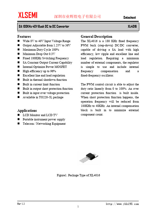
8A 180KHz 40V Buck DC to DC Converter XL4016FeaturesnWide 8V to 40V Input Voltage Range n Output Adjustable from 1.25V to 36V n Maximum Duty Cycle 100% n Minimum Drop Out 0.3Vn Fixed 180KHz Switching Frequency n 8A Constant Output Current Capability n Internal Optimize Power MOSFET n High efficiency up to 96%n Excellent line and load regulation n Built in thermal shutdown function n Built in current limit functionn Built in output short protection function n Built in input over voltage protection n Available in TO220-5L packageApplicationsn LCD Monitor and LCD TVn Portable instrument power supply n Telecom / Networking EquipmentGeneral DescriptionThe XL4016 is a 180 KHz fixed frequency PWM buck (step-down) DC/DC converter, capable of driving a 8A load with high efficiency, low ripple and excellent line and load regulation. Requiring a minimum number of external components, the regulator is simple to use and include internal frequency compensation and a fixed-frequency oscillator.The PWM control circuit is able to adjust the duty ratio linearly from 0 to 100%. An over current protection function is built inside. When short protection function happens, the operation frequency will be reduced from 180KHz to 48KHz. An internal compensation block is built in to minimize external component count.Figure1. Package Type of XL40168A 180KHz 40V Buck DC to DC ConverterXL4016Pin ConfigurationsFigure2. Pin Configuration of XL4016 (Top View) Table 1 Pin DescriptionPin Number Pin Name Description1 GND Ground Pin. Care must be taken in layout. This pin should be placed outside of the Schottky Diode to output capacitor ground path to prevent switching current spikes from inducing voltage noise into XL4016.2 FB Feedback Pin (FB). Through an external resistor divider network, FB senses the output voltage and regulates it. The feedback threshold voltage is 1.25V.3 SW Power Switch Output Pin (SW). SW is the switch node that supplies power to the output.4 VC Internal V oltage Regulator Bypass Capacity. In typical system application, The VC pin connect a 1uf capacity to VIN.5 VIN Supply V oltage Input Pin. XL4016 operates from a 8V to 40V DC voltage. Bypass Vin to GND with a suitably large capacitor to eliminate noise on the input.8A 180KHz 40V Buck DC to DC Converter XL4016 Function BlockFigure3. Function Block Diagram of XL4016Typical Application CircuitFigure4. XL4016 Typical Application Circuit (VIN=8V~40V, VOUT=5V/8A)8A 180KHz 40V Buck DC to DC Converter XL4016 Ordering InformationPart Number Marking ID Lead Free Lead Free Packing TypePackage TemperatureRangeXL4016E1 XL4016E1 TubeXLSEMI Pb-free products, as designated with “E1” suffix in the par number, are RoHS compliant.Absolute Maximum Ratings(Note1)Parameter Symbol Value Unit Input Voltage Vin -0.3 to 45 V Feedback Pin Voltage V FB-0.3 to Vin V Output Switch Pin Voltage V Output-0.3 to Vin V Power Dissipation P D Internally limited mW Thermal Resistance (TO220-5L)(Junction to Ambient, No Heatsink, Free Air)R JA30 ºC/W Operating Junction Temperature T J-40 to 125 ºC Storage Temperature T STG-65 to 150 ºC Lead Temperature (Soldering, 10 sec) T LEAD260 ºC ESD (HBM) >2000 V Note1: Stresses greater than those listed under Maximum Ratings may cause permanent damage to the device. This is a stress rating only and functional operation of the device at these or any other conditions above those indicated in the operation is not implied. Exposure to absolute maximum rating conditions for extended periods may affect reliability.8A 180KHz 40V Buck DC to DC Converter XL4016 XL4016 Electrical CharacteristicsT a = 25℃;unless otherwise specified.Symbol Parameter Test Condition Min. Typ. Max. Unit System parameters test circuit figure4VFB FeedbackV oltageVin = 8V to 40V, V out=5VIload=0.5A to 8A1.225 1.25 1.275 VEfficiency ŋVin=12V ,V out=5VIout=6A- 87 - %Efficiency ŋVin=24V ,V out=12VIout=6A- 93 - %Electrical Characteristics (DC Parameters)Vin = 12V, GND=0V, Vin & GND parallel connect a 470uf/50V capacitor; Iout=500mA, T a = 25℃; the others floating unless otherwise specified.Parameters Symbol Test Condition Min. Typ. Max. Unit Input operation voltage Vin 8 40 V Quiescent Supply Current I q V FB =Vin 2.1 5 mA Oscillator Frequency Fosc 144 180 216 KHz Output Short Frequency Fosp 48 KHz Switch Current Limit I L V FB =0 10 A Max. Duty Cycle D MAX V FB=0V 100 %Output Power PMOS Rdson V FB=0V, Vin=12V,I SW=8A40 50 mohmVin Over V oltage Protection OVP 45 V8A 180KHz 40V Buck DC to DC ConverterXL4016Typical System Application (VOUT=5V/8A)Figure5. XL4016 System Parameters Test Circuit (VIN=8V~40V, VOUT=5V/8A)50556065707580859095100Efficiency VS Load currentE f f i c i e n c y (%)Load current(A)Figure6. XL4016 System Efficiency Curve8A 180KHz 40V Buck DC to DC ConverterXL4016Typical System Application (VOUT=12V/6A)Figure7. XL4016 System Parameters Test Circuit (VIN=15V~40V, VOUT=12V/6A)0.00.51.01.52.02.53.03.54.04.55.05.56.050556065707580859095100Efficiency VS Load currentE f f i c i e n c y (%)Load current(A)Figure8. XL4016 System Efficiency Curve8A 180KHz 40V Buck DC to DC Converter XL4016Typical System Application (With Enable function)Logic level signal shutdown function can be used in typical system application with externalcomponents. When the TTL high voltage above 3.3V(referenced to ground, lower than VIN), the converter will shutdown, input current less than 3mA; when theTTL Low voltage below 0.8V(referenced to ground), the converter will turn on.L1 47uH/12AFigure9. XL4016 Typical Application Circuit with Enable Function8A 180KHz 40V Buck DC to DC Converter XL4016Package InformationTO220-5L。
cd4016b工作原理

cd4016b工作原理CD4016B工作原理什么是CD4016BCD4016B是一种集成电路(IC),它是一种四路双控开关。
它广泛应用于模拟信号开关、模拟多路选择和数字逻辑开关等领域。
引脚功能说明CD4016B一共有14个引脚,其中8个用于开关控制,6个用于信号传输。
以下是各引脚的功能:1.IN1-IN4:四个输入引脚,用于控制开关的通断。
2.OUT1-OUT4:四个输出引脚,用于输出被开关的信号。
3.VDD、VSS:正电源和地引脚。
4.VEE、SUB:负电源引脚。
5.E1、E2:两个输出使能引脚,用于控制开关的工作状态。
工作原理解析CD4016B的工作原理是基于CMOS(互补型金属氧化物半导体)技术实现的。
它内部包含了一组开关电路,可以通过控制输入引脚的电压来切换信号的通断。
当E1和E2引脚的电压都为高电平时(通常为VDD),开关才能工作。
此时,IN1-IN4引脚的电压决定了开关的状态。
当某个输入引脚的电压为高电平时,对应的开关闭合,将输入信号直接传输到对应的输出引脚上。
需要注意的是,CD4016B是一种双控开关,即需要同时满足E1和E2引脚的电压要求才能使开关工作。
这种设计可以有效地防止误操作和干扰,提高了开关的可靠性。
应用领域CD4016B广泛应用于模拟信号开关、模拟多路选择和数字逻辑开关等领域。
它可以实现对模拟信号的多路选择和切换,同时也可以作为数字逻辑电路的关键部分。
在模拟电路中,CD4016B可以用于音频信号的切换、模拟开关矩阵等应用。
在数字电路中,它可以作为数字信号的选择器、数据交换器等功能模块的组成部分。
总结CD4016B是一种双控四路开关集成电路,采用CMOS技术实现。
通过控制输入引脚的电压,可以实现对模拟信号的切换和选择。
它在模拟电路和数字电路中有着广泛的应用,是一种功能强大且可靠的电路元件。
通过以上对CD4016B的工作原理的解析,我们对这种集成电路有了更深入的了解。
希望本文对您有所帮助!CD4016B的特点CD4016B采用CMOS技术,具有以下特点:1.低功耗:由于采用CMOS技术,CD4016B的功耗非常低,适用于对功耗要求较高的应用场景。
- 1、下载文档前请自行甄别文档内容的完整性,平台不提供额外的编辑、内容补充、找答案等附加服务。
- 2、"仅部分预览"的文档,不可在线预览部分如存在完整性等问题,可反馈申请退款(可完整预览的文档不适用该条件!)。
- 3、如文档侵犯您的权益,请联系客服反馈,我们会尽快为您处理(人工客服工作时间:9:00-18:30)。
ASCEND Semiconductor 4Mx4 EDO Data sheetDescriptionThe device CMOS Dynamic RAM organized as 4,194,304 words x 4 bits with extended data out access mode. It is fabricated with an advanced submicron CMOS technology and designed to operate from a single 3.3V oniy power supply. Low voltage operation is more suitable to be used on battery backup, portable elec-tronic application. lt is packaged in JEDEC standard 26/24-pin plastic SOJ or TSOP(II).Features• Single 3.3V(%) only power supply • High speed t RAC acess time: 50/60ns • Low power dissipation- Active mode : 432/396 mW (Mas) - Standby mode: 0.54 mW (Mas)• Extended - data - out(EDO) page mode access • I/O level: CMOS level (Vcc = 3.3V)• 2048 refresh cycle in 32 ms(Std.) or 128 ms(S-version)• 4 refresh modesh: - RAS only refresh- CAS - before - RAS refresh - Hidden refresh - Self-refresh(S-version)10±Pin Name FunctionA0-A10Address inputs- Row address - Column address - Refresh address DQ1~DQ4Data-in / data-out RAS Row address strobe CAS Column address strobe WE Write enable OE Output enable Vcc Power (+ 3.3V)VssGroundVCC 1DQ12DQ23DQ34DQ45VCC6891011 NC 12 WE 13A0 A117 A218 A319VSS RAS CAS OE A8A7A6A5A4VSSAD404M42VSPin Description Pin Configuration21222324 2526151416 A1026/24-PIN 300mil Plastic SOJA9VCC 1DQ12DQ23DQ34DQ45VCC6891011 NC 12 WE 13A0 A117 A218 A319VSS RAS CAS OE A8A7 A6A5 A4VSSAD404M42VT212223242526151416 A1026/24-PIN 300mil Plastic TSOP (ll)A9A0-A10A0-A10A0-A10WECASNO. 2 CLOCK GENERATORCOLUMN ADDRESS BUFFERS (11)REFRESH CONTROLLERREFRESH COUNTERBUFFERS (11)ADDRESS ROW NO. 1 CLOCK GENERATORA0RASA1A2A3A4A5A6A7A8CONTROLLOGICDATA-IN BUFFERDATA-OUT BUFFEROEDQ1.DQ4.COLUMN DECODER2048SENSE AMPLIFIERSI/O GATING2048x42048x2048x4MEMORY ARRAY2048R O W D E C O D E RVcc VssBlock DiagramA9A10TRUTH TABLENotes: 1. EARLY WRITE only.FUNCTIONRASCAS WE OE ADDRESSESDQ SNotesROW COL STANDBY H X X X X High-Z READL L H L ROW COL Data-Out WRITE: (EARLY WRITE )L L L X ROW COL Data-lnREAD WRITE L L ROW COL Data-Out,Data-ln EDO-PAGE-MODE READ1st Cycle L H L ROW COL Data-Out 2nd CycleL H L n/a COL Data-Out EDO-PAGE MODE WRITE1st CycleL L X ROW COL Data-In 2nd Cycle L L Xn/a COL Data-InEDO-PAGE-MODEREAD-WRITE 1st Cycle L ROW COL Data-Out, Data-In 2nd Cycle L n/a COL Data-Out, Data-In HIDDEN REFRESHREAD L H L ROW COL Data-Out WRITEL L X ROW COL Data-In 1RAS-ONLY REFRESH L H X X ROW n/a High-Z CBR REFRESHLHXXXHigh-ZH X →H L →L H →H L →H L →H L →H L →H L →H L →L H →H L →H L →L H→L H L →→L H L→→H L→Absolute Maximum RatingsRecommended DC Operating ConditionsCapacitanceTa = 25°C, V CC = 3.3V%, f = 1MHz Note: 1. Capacitance measured with effective capacitance measuring method. 2. RAS, CAS = V IH to disable Dout.ParameterSymbol Value Unit Voltage on any pin relative to Vss V T -0.5 to + 4.6V Supply voltage relative to Vss V CC -0.5 to + 4.6V Short circuit output current I OUT 50mA Power dissipation P D 1.0WOperating temperature T OPT 0 to + 70°C Storage temperatureT STG-55 to + 125°CParameter/Condition Symbol3.3 Volt VersionUnitMinTyp MaxSupply VoltageV CC 3.0 3.33.6V Input High Voltage, all inputs V IH 2.0-V CC + 0.3V Input Low Voltage, all inputsV IL-0.3-0.8VParameterSymbol Typ Max Unit Note Input capacitance (Address)C I1 -5pF 1Input capacitance (RAS, CAS, OE, WE)C I2-7pF 1Output capacitance(Data-in, Data-out)C I/O-7pF1, 210±DC Characteristics :(T a = 0 to 70°C, V CC = + 3.3V%, V SS = 0V)Parameter Symbol Test Conditions AD404M42V Unit Notes-5-6Min Max Min MaxOperating current I CC1RAS cyclingCAS, cyclingt RC = min-120-110mA1, 2Standby Current LowpowerS-versionI CC2LVTTL interfaceRAS, CAS = V IHDout = High-Z-0.5-0.5mACMOS interfaceRAS, -0.2VDout = High-Z-0.15-0.15mAStandardpowerversionLVTTL interfaceRAS, CAS = V IHDout = High-Z-2-2mACMOS interfaceRAS,-0.2VDout = High-Z-0.5-0.5mARAS- only refresh current I CC3RAS cycling, CAS = V IHt RC = min-120-110mA1, 2 EDO page mode current I CC4t PC = min-90-80mA1, 3CAS- before- RAS refresh current I CC5t RC = minRAS, CAS cycling-120-110mA1, 2Self- refresh current (S-Version)I CC8 - 550 - 55010±CAS V CC≥CAS V CC≥t RASS100µs≥µADC Characteristics :(T a = 0 to 70°C , V CC = +3.3V %, V SS = 0V)Notes:1. I CC is specified as an average current. It depends on output loading condition and cycle rate when the device is selected. I CC max is specified at the output open condition.2. Address can be changed once or less while RAS = V IL .3. For I CC4, address can be changed once or less within one EDO page mode cycle time.Parameter Symbol Test Conditions AD404M42VUnitNotes-5-6Min MaxMin MaxInput leakage current I LI + 0.3V -55-55Output leakage current I LO + 0.3V Dout = Disable -55-55Output high Voltage V OH I OH = -2mA 2.4- 2.4-V Output low voltage V OLI OL = +2mA-0.4-0.4V10±0V Vin V CC ≤≤µA 0V Vout V CC ≤≤µAAC Characteristics(T a = 0 to + 70°C , V cc = 3.3V %, V ss = 0V) *1, *2, *3, *4Test conditions• Output load: one TTL Load and 100pF (V CC = 3.3V %)• Input timing reference levels:V IH = 2.0V, V IL = 0.8V (V CC = 3.3V %)• Output timing reference levels:V OH = 2.0V, V OL = 0.8V10±10±10±Read, Write, Read- Modify- Write and Refresh Cycles (Common Parameters)ParameterSymbol AD404M42V UnitNotes-5-6Min MaxMin MaxRandom read or write cycle time t RC 84-104-ns RAS precharge timet RP 30-40-ns CAS precharge time in normal mode t CPN 10-10-ns RAS pulse width t RAS 50100006010000ns 5CAS pulse width t CAS 8100001010000ns 6Row address setup time t ASR 0-0-ns Row address hold time t RAH 8-10-ns Column address setup time t ASC 0-0-ns 7Column address hold time t CAH 8-10-ns RAS to CAS delay timet RCD 12371445ns 8RAS to column address delay time t RAD 10251230ns 9Column address to RAS lead time t RAL 25-30-ns RAS hold time t RSH 8-10-ns CAS hold timet CSH 38-40-ns CAS to RAS precharge time t CRP 5-5-ns 10OE to Din delay time t OED 12-15-ns Transition time (rise and fall)t T 150150ns 11Refresh periodt REF -32-32ms Refresh period (S- Version)t REF -128-128ms CAS to output in Low- Z t CLZ 0-0-ns CAS delay time from Din t DZC 0-0-ns OE delay time from Dint DZO-0-nsRead CycleWrite Cycle Parameter SymbolAD404M42V Unit Notes-5-6Min Max Min MaxAccess time from RAS t RAC-50-60ns12 Access time from CAS t CAC-14-15ns13, 14 Access time from column address t AA-25-30ns14, 15 Access time from OE t OEA-12-15nsRead command setup time t RCS0-0-ns7 Read command hold time to CAS t RCH0-0-ns10, 16 Read command hold time to RAS t RRH0-0-ns16 Output buffer turn-off time t OFF012015ns17 Output buffer turn-off time from OE t OEZ012015ns17Parameter SymbolAD404M42V Unit Notes -5-6Min Max Min MaxWrite command setup time t WCS0-0-ns7, 18 Write command hold time t WCH8-10-nsWrite command pulse width t WP8-10-nsWrite command to RAS lead time t RWL13-15-nsWrite command to CAS lead time t CWL8-10-nsData-in setup time t DS0-0-ns19 Data-in hold time t DH8-10-ns19 WE to Data-in delay t WED10-10-nsRead- Modify- Write CycleRefresh Cycle Parameter SymbolAD404M42V Unit Notes-5-6Min Max Min MaxRead-modify- write cycle time t RWC108-133-nsRAS to WE delay time t RWD64-77-ns18 CAS to WE dealy time t CWD26-32-ns18 Column address to WE delay time t AWD39-47-ns18 OE hold time from WE t OEH8-10-nsParameter SymbolAD404M42VUnit Notes -5-6Min Max Min MaxCAS setup time (CBR refresh) t CSR5-5-nsCAS hold time (CBR refresh)t CHR8-10-ns10 RAS precharge to CAS hold time t RPC5-5-ns7 RAS pulse width (self refresh)t RASS100-100-RAS precharge time (self refresh)t RPS90-110-nsCAS hold time (CBR self refresh)t CHS-50--50-nsWE setup time t WSR0-0-nsWE hold time t WHR10-10-nsµsEDO Page Mode CycleEDO Page Mode Read Modify Write CycleParameterSymbol AD404M42VUnit Notes-5-6Min MaxMin MaxEDO page mode cycle timet PC 20-25-ns EDO page mode CAS precharge time t CP 10-10-ns EDO page mode RAS pulse width t RASP 5010560105ns 20Access time from CAS precharge t CPA -30-35ns 10, 14RAS hold time from CAS precharge t CPRH 30-35-ns OE high hold time from CAS high t OEHC 5-5-ns OE high pulse widtht OEP 10-10-ns Data output hold time after CAS low t COH 5-5-ns Output disable delay from WEt WHZ 310310ns WE pulse width for output disable whenCAS hight WPZ7-7-nsParameterSymbol AD404M42V Unit Notes -5-6Min MaxMin MaxEDO page mode read- modify- write cycle CAS precharge to WE delay timet CPW 45-55-ns 10EDO page mode read- modify- write cycle timet PRWC56-68-nsNotes :1. AC measurements assume t T = 2ns.2. An initial pause of 100 is required after power up, and it followed by a minimum of eightinitialization cycles (RAS - only refresh cycle or CAS - before - RAS refresh cycle). If the internal refresh counter is used, a minimun of eight CAS - before - RAS refresh cycles are required.3. In delayed write or read-modify-write cycles, OE must disable output buffer prior to applying data to the device.4. All the V CC and V SS pins shall be supplied with the same voltages.5. t RAS (min) = t RWD (min)+t RWL (min)+t T in read-modify-write cycle.6. t CAS (min) = t CWD (min)+t CWL (min)+t T in read-modify-write cycle.7. t ASC (min), t RCS (min), t WCS (min), and t RPC are determined by the falling edge of CAS .8. t RCD (max) is specified as a reference point only, and t RAC (max) can be met with the t RCD (max) limit.Otherwise, t RAC is controlled exclusively by t CAC if t RCD is greater than the specified t RCD (max) limit. 9. t RAD (max) is specified as a reference point only, and t RAC (max) can be met with the t RAD (max) limit.Otherwise, t RAC is controlled exclusively by t AA if t RAD is greater than the specified t RAD (max) limit. 10. t CRP , t CHR , t RCH , t CPA and t CPW are determined by the rising edge of CAS .11. V IH (min) and V IL (max) are reference levels for measuring timing or input signals. Therefore, transitiontime is measured between V IH and V IL .12. Assumes that t RCD tRCD (max) and t RAD t RAD (max). If t RCD or t RAD is greater than the maximum recommended value shown in this table, t RAC exceeds the value shown. 13. Assumes that (max) and (max).14. Access time is determined by the maximum of t AA , t CAC , t CPA . 15. Assumes that (max) and (max). 16. Either t RCH or t RRH must be satisfied for a read cycle.17. t OFF (max) and t OEZ (max) define the time at which the output achieves the open circuit condition (highimpedance). t OFF is determined by the later rising edge of RAS or CAS.18. t WCS , t RWD , t CWD , and t AWD are not restrictive operating parameters. They are included in the datasheet as electrical characteristics only. If (min), the cycle is an early write cycle and the data out will remain open circuit (high impedance) throughout the entire cycle. If (min),(min), (min) and (min), the cycle is a read-modify-write and the data output will contain data read from the selected cell. If neither of the above sets of conditions is satisfied, the condition of the data output (at access time) is indeterminate.19. These parameters are referenced to CAS separately in an early write cycle and to WE edge in adelayed write or a read-modify-write cycle.20. t RASP defines RAS pulse width in EDO page mode cycles.µs ≤≤t RCD t RCD ≥t RADt RAD ≤t RCD t RCD ≤t RAD t RAD ≥t WCS t WCS ≥t RWD t RWD ≥t CWDt CWD ≥t AWD t AWD ≥t CPW t CPW≥Timing Waveforms• Read Cyclet RC t RASt RPtCRPtCPNtRRHtRCHt OEZ t OFF tOEA tCACt AAtRACt CLZD OUTtRCS t ASR tRAH tASC tCAH tRAD t RALtCAStRSH tRCDt TtCSHRASCASADDRESSWEDQ1~DQ4Note : = don’t care OEt OFFRowColumn= Invalid Dout•Early Write CycletRC t RASt RPt WCHt DSt DHt WCS t RALtCAStRSH tRCDt TtCSHRASCASWEDQ1~DQ4tCRPtASRtRAH tASCtCAH ADDRESSColumnRowtCPND INtRADt RAL• Delayed Write CycletRC t RASt RPt RWL t RCSt CAStRSH tRCDt TtCSHRASCAStASR tRAH tCAHADDRESSColumnRow tASC D INDQ1~DQ4WEtCRPtCPNt DHt DSt OEHt OEDOEt DSOPENt WPt CWL• Read - Modify - Write CycletRWC t RASt RPtRWDt WPtRADtRWL tCAStCWL tRCDt TtCPNRASCASWEtCRP t ASRtRAHtASCtCAHADDRESS Column RowDQ1~DQ4t DHt DSOEtRCStAWD tCWD D INt OEDt OEHt OEZt OEA t CAC t RACt AADQ1~DQ4D OUTOPENtDZCtDZO• EDO Page Mode Read CycletRASPtCPRHt RCStCAStRSH tRCDt OEAtCSHRASCAStASRtRAHtCAHADDRESStCASWEtCRPt CPOEDQ1~DQ4OPENtOEPD OUT 1t PCt CPtCAStCPNtCRPtRADtCAHtASCt ASCtCAHt ASCt RAL Row Column 1t OEAt OEHCtRRH tRCHt RACt AAt AAt AA t CPA t CPA t OEZt OFFt OFFt CACt OEZt CAC t CACt COHD OUT NWE OE Column 2Column N Rowt RPD OUT 2• EDO Page Mode Early Write CycletRASPtRPt WCSt CAStRSH tRCDRASCAStASRtRAHtCAHADDRESStCASWEt CPDQ1~DQ4t PCt CPt CAStCPNtCRP tCAH tASCtASC tCAH tASC Row Column 1t DS WE Column 2Column Nt WCH t WCS t WCH t WCS t WCHt DH t DS t DH t DS t DHD IN 1D IN 2D IN Nt TtCSH• EDO Page Mode Read-Early-Write Cyclet RASPtCPRHt RCStCAStRSH tRCDt OEAtCSHRASCAStASRtRAHtCAHADDRESStCASWEtCRPt CPOEDQ1~DQ4OPENtWEDt PCt CPtCAStCPNtCRPtRADtRAHtASCt ASCtCAHt ASCt RAL Row Column 1tWCStRCHt RACt AAt AAt CPA t DHt WHZt CACt CACt COHWE OE Column 2Column N Rowt RPt CAL tWCHDataDoutput 2Data Input NDataDoutput 1t DStCSH• EDO Page Mode Read-Modify-Write Cyclet RASPt CPRHt RCStCASt WP RASCASt ASRtRAHtCAHADDRESSt CASWEtRCDCPDQ1~DQ4tPRWCt CPtCAStCRPtRADtCAHtASCt ASCtCAH tASC Row Column 1tRWLtRCSt OEDt DZOt CAC WE OEt RPt RAL D OUT 2D OUT ND OUT 1tTt Column NColumn 2Column 1tRWD tAWD tCWDtCWLtRCStCWDtAWD tCPW tCWL tCPW tAWD tCWDtCWL t OEDt OEDt OEHt OEHt OEHt CAC t CAC t OEA t AAt RACt OEZt OEAt AA t CPAt OEZt OEAt AA t CPAt OEZ t DSt DHt WP t DSt DHt WP t DSt DHOPENOPENOPEN D IN 1D IN ND IN 2DQ1~DQ4t DZCt DZOt DZCt DZCt DZO• Read Cycle with WE Controlled Disablet WPZt RCStCAStRCDt TtCSHRASCASt ASRtRAHtCAHADDRESSColumnRow tASCD DQ1~DQ4WEt OEZt DSt WHZOEt RCH t OEA t CACt AAt RACt CLZOUTtRADRASADDRESSt RC t CRPt ASRt RAHt Tt RPCROWt OFFCAS t RASt RPOPENt CRPDQ1~DQ4RASt CSRt WSRt RPt T t RPCt OFFCAS t RASt RPOPENt CRPDQ1~DQ4t RPCt CHRt RASt RPt RCt RCt CHRt CSRt WHRt WSRt WHRWECAS-Before-RAS Refresh CycleRASWEt RPCt OFFt CSRt CHSt WSRCASt RASS t RPSOPENDQ1~DQ4t WHRHigh lmpedance• Hidden Refresh Cyclet RPt RASRASt RCDt CRPADDRESSWEt CHRt CASt RSHt RAHt ASRt ASCt CAHt RAL ROW t RCHt OEZCASDQ1~DQ4t Tt RCSD t RASt RASt RPt RPt RC t RCt RCt RADt RRHt OFF t OFFt OEA t CACt AAt RACCOlumnOUTOE(READ)(REFRESH)(REFRESH)Ordering informationAD404M42VSA-5• AD• Ascend Memory Product • 40 • Device Type• 4M4 • Density and Organization • 2• Refresh Rate, 2: 2K Refresh • V• T: 5V, V: 3.3V• S • Package Type (S : SOJ, T : TSOP II)• A• Version• 5• Speed (5: 50 ns, 6: 60 ns)Part Number Access time PackageAD404M42VSA-5AD404M42VSA-6AD404M42VTA-5AD404M42VTA-650 ns 60 ns 50 ns 60 ns300mil 26/24-Pin Plastic SOJTSOP IIPackaging information • 300 mil, 26/24-Pin Plastic SOJ• 300 mil, 26/24-Pin TSOP II。