LB11867FV-TLM-H;LB11867FV-TLM-E;中文规格书,Datasheet资料
e-switch 产品说明书

RoHSN A V I G A T I S W I T C H E R O C K E R S W I T C H E S R O T A R Y S W I T C H E S S L I D E S W I T C H E S S N A P A C T I O N S W I T C H E ST A C T I L E SW I T C H E ST O G G L E S W I T C H E S C A P O P T I O N S P U S H B U T T O N S W I T C H E SAudio / Visual Security Devices Industrial ControlsElectrical Housewares Kiosks SpecificationsFeatures & BenefitsApplications / Markets• 19mm diameter panel cutout • RGB LED option• Dot, ring or power symbol illumination available • Multiple function options • IP65 rated • SPDT & DPDT•Soldered wire leads (300mm long) optionalElectrical Rating: 2A, 24VDC Electrical Life: 50,000 CyclesContact Resistance: 50mΩ Max. Insulation Resistance: 1000 MΩ Min. Dielectric Strength: 2,000VACOperating/Storage Temperature: -20°C to 55°C Travel: 2.50mm Moisture Protection: IP65Contact Arrangement: SPDT, DPDT Actuation Force: 4 NPanel Thickness: 1-11mmMounting Nut Torque: 5-14NmMedical EquipmentANTI-VANDAL SWITCHES DETECTOR SWITCHESDIP SWITCHESKEYLOCK SWITCHESROCKER SWITCHES ROTARY SWITCHESSLIDE SWITCHES SNAP ACTION SWITCHESTACTILE SWITCHES TOGGLE SWITCHESCAP OPTIONSNAVIGATION SWITCHESPUSHBUTTON SWITCHESANTI-VANDAL SWITCHESStandard LEDFunctions 3, B, G & HSPDT LED SchematicRECOMMENDED "D" PANEL CUTOUTMAX. PANEL THICKNESS 11.0mm "D" HOUSING TO BE USED WITHPOWER SYMBOL OR CUSTOM GRAPHICSRECOMMENDED PANEL CUTOUTMAX. PANEL THICKNESS 11.0mmDPDT ILLUMINATED OPTION SHOWN LED (+) AND (-)TERMINALS ARE NOT INCLUDED ON THENON-ILLUMINATED OPTIONTERMINALS 4,5 AND 6 ARE NOT ON THE SPDT VERSIONFUNCITONS 3 & B ARE SPDT FUNCTIONS G & H ARE DPDT18.45 .15.726 .006 in []19.00 -.00.20+.748-.000.008+ in[]-(REVERSE)(FORWARD)(-)+-2311(+)+231119.00 -.00.20+.748-.000.008+ in[]11443265(+)-(REVERSE)+(FORWARD)-(-)+1144326536.9 1.01.45 .04 in []1.80[.071 in]M19 X 1.038.0 1.01.50 .04 in []22.00[ .866 in]15.80[ .622 in]13.60[ .535 in]RING ILLUMINATED(OPTIONAL)12.00[.472 in].50[.020 in](+)(-)TERMINAL 6TERMINAL 5TERMINAL 4TERMINAL 3TERMINAL 2TERMINAL 15.20[.205 in]10.00[.394 in]2.80[.110 in]SPDT Non Ill SchematicDPDT LED SchematicDPDT Non Ill SchematicS W I T C H E SD E T E C T O R S W I T C H E SD I P S W I T C HE SK E Y L O C K S W I T C H E SN A V I G A T I O N S W I T C H E SP U S H B U T T O N S W I T C H E SR O C K E R S W I T C H E SR O T A R Y S W I T C H E S S L I D E S W I T C H E SS N A P A C T I O N S W I T C H E S T A C T I L E S W I T C H E ST O G G L E S W I T C H E SC A P O P T I O N SA N T I -V A N D A L S W I T C H E S Y Function w/Solder TerminalsSPDT LED SchematicSPDT Non Ill SchematicRECOMMENDED "D" PANEL CUTOUTMAX. PANEL THICKNESS 11.0mm "D" HOUSING TO BE USED WITHPOWER SYMBOL OR CUSTOM GRAPHICSRECOMMENDED PANEL CUTOUTMAX. PANEL THICKNESS 11.0mm4+1-(REVERSE)(FORWARD)(-)+-4231(+)+19.00 -.00.20+.748-.000.008+ in[]18.45 .15.726 .006 in []19.00 -.00.20+.748-.000.008+ in[]4231RING ILLUMINATION(OPTIONAL)22.00[.866 in]12.0[.47 in]15.4[.606 in]ILLUMINATED OPTION SHOWN LED (+) AND (-) TERMINALS ARE NOT ON THE NON-ILLUMINATED OPTIONM19 X 1.03.80[.150 in] 2.00[.079 in]33.4 1.01.31 .04 in []9.80[.386 in](+)(-)7.60[.299 in] 2.80[.110 in].50[.020 in]7.60[.299 in]TERMINAL 1TERMINAL 3TERMINAL 2TERMINAL 4ANTI-VANDAL SWITCHESDETECTOR SWITCHESDIP SWITCHESKEYLOCK SWITCHESNAVIGATION SWITCHESPUSHBUTTON SWITCHESROCKER SWITCHESROTARY SWITCHES SLIDE SWITCHES SNAP ACTION SWITCHESTACTILE SWITCHES TOGGLE SWITCHESCAP OPTIONSANTI-VANDAL SWITCHES Y Function w/Screw TerminalsRECOMMENDED "D" PANEL CUTOUTMAX. PANEL THICKNESS 11.0mm "D" HOUSING TO BE USED WITHPOWER SYMBOL OR CUSTOM GRAPHICSRECOMMENDED PANEL CUTOUTMAX. PANEL THICKNESS 11.0mm-(REVERSE)(FORWARD)(-)+-4231(+)+423119.00 -.00.20+.748-.000.008+ in[]18.45 .15.726 .006 in []19.00 -.00.20+.748-.000.008+ in[] 22.00[ .866 in]15.40[ .606 in]12.00[ .472 in]RING ILLUMINATED(OPTIONAL)M19 X 1.02.00[.079 in]34.6 1.01.36 .04 in []15.60[.614 in](+)TERMINAL 4TERMINAL 2(-)TERMINAL 1TERMINAL 39.60[.378 in]7.60[.299 in]7.60[.299 in]SPDT LED SchematicSPDT Non Ill SchematicA S W I T C H E SD E T E C T O R S W I T C H E SD I P S W I T C HE SK E Y L O C K S W I T C H E SN A V I G A T I O N S W I T C H E S P U S H B U T T O N S W I T C H E S R O C K E R S W I T C H E SR O T A R Y S W I T C H E S S L I D E S W I T C H E S S N A P A C T I O N S W I T C H E S T A C T I L E S W I T C H E ST O G G L E S W I T C H E SC A P O P T I O N SN T I -V A N D A L S W I T C H E S RGB Led IlluminationFunctions 3 & BRECOMMENDED "D" PANEL CUTOUTMAX. PANEL THICKNESS 11.0mm "D" HOUSING TO BE USED WITHPOWER SYMBOL OR CUSTOM GRAPHICSRECOMMENDED PANEL CUTOUTMAX. PANEL THICKNESS 11.0mm1.8[.07 in]36.9 1.01.45 .04 in [].50[.020 in]38.0 1.01.50 .04 in []RED (+)GREEN (+)BLUE (+)(-)121319.00 -.00.20+.748-.000.008+ in[]18.45 .15.726 .006 in []19.00 -.00.20+.748-.000.008+ in[]12.00[.472 in] 22.00[ .866 in]15.80[ .622 in]13.60[ .535 in]RING ILLUMINATION(OPTIONAL)RED (+)GREEN (+)BLUE (+)(-)TERMINAL 1TERMINAL 2TERMINAL 35.20[.205 in]10.00[.394 in]2.80[.110 in]SPDT RGB LED SchematicANTI-VANDAL SWITCHES DETECTOR SWITCHESDIP SWITCHESKEYLOCK SWITCHESNAVIGATION SWITCHESPUSHBUTTON SWITCHES ROCKER SWITCHESROTARY SWITCHES SLIDE SWITCHESSNAP ACTION SWITCHESTACTILE SWITCHES TOGGLE SWITCHES CAP OPTIONSPUSHBUTTON SWITCHES ANTI-VANDAL SWITCHESActuator OptionsGraphic OptionsFlat Non-Illuminated Flat Dot Illuminated Flat Ring IlluminatedORIENTATION FLAT FOR GRAPHIC8.00[.315 in]ORIENTATION FLAT FOR GRAPHICRINGILLUMINATIONDOTILLUMINATION9.00[.354 in]6.0[.24 in]1.60[.063 in]22.00[ .866 in] 15.40[ .606 in]22.00[ .866 in]22.00[ .866 in]15.80[ .622 in] 13.60[ .535 in]ILLUMINATED8.00[.315 in]LASER ETCHED 6.50[.256 in]High ActuatorFlat ActuatorA S W I T C H E SD E T E C T O R S W I T C H E SD I P S W I T C HE S K E Y L O C K S W I T C H E S N A V I G A T I O N S W I T C H E S P U S H B U T T O N S W I T C H E SR O C K E R S W I T C H E SR O T A R Y S W I T C H E SS L I D E S W I T C H E S S N A P A C T I O NS W I T C H E S T A C T I L E S W I T C H E ST O G G L E S W I T C H E SC A P O P T I O N SN T I -V A N D A L S W I T C H E S Standard LEDWire LeadRECOMMENDED "D" PANEL CUTOUTMAX. PANEL THICKNESS 11.0mm "D" HOUSING TO BE USED WITHPOWER SYMBOL OR CUSTOM GRAPHICSRECOMMENDED PANEL CUTOUTMAX. PANEL THICKNESS 11.0mmBOTTOM VIEW SHOWN WITHOUTWIRING** WIRE LEADS PROVIDED ARE DEPENDANT ON THE FUNCTION AND/OR ILLUMINATION SELECTED **19.00 -.00.20+.748-.000.008+ in[]18.45 .15.726 .006 in []19.00 -.00.20+.748-.000.008+ in[]13.0 2.0.5 .1 in []300.0 10.011.8 .4 in [](8) WIRE, 24 AWG,AWM UL1015 WITH ENDS PRE-STRIPPEDHEATSHRINK OVER SOLDERED CONNECTIONSWIRE TIE25.4[1.0 in]()(-)TERMINAL 3(+)SWITCH WIRELENGTH SW1-1WIRE, 24AWG AWM UL1015, YELLOW 300.0 [11.8 in]SW1-2WIRE, 24AWG AWM UL1015, BLUE 300.0 [11.8 in]SW1-3WIRE, 24AWG AWM UL1015, GREEN 300.0 [11.8 in]SW1-4WIRE, 24AWG AWM UL1015, PURPLE 300.0 [11.8 in]SW1-5WIRE, 24AWG AWM UL1015, ORANGE 300.0 [11.8 in]SW1-6WIRE, 24AWG AWM UL1015, WHITE 300.0 [11.8 in]SW1- (+)WIRE, 24AWG AWM UL1015, RED 300.0 [11.8 in]SW1- (-)WIRE, 24AWG AWM UL1015, BLACK300.0 [11.8 in]TERMINAL 1TERMINAL 2TERMINAL 4TERMINAL 5TERMINAL 615.0 2.0.6 .1 in []ANTI-VANDAL SWITCHES DETECTOR SWITCHES DIP SWITCHES KEYLOCK SWITCHESNAVIGATION SWITCHESPUSHBUTTON SWITCHES ROCKER SWITCHESROTARY SWITCHESSLIDE SWITCHES SNAP ACTION SWITCHESTACTILE SWITCHES TOGGLE SWITCHESCAP OPTIONSPUSHBUTTON SWITCHES ANTI-VANDAL SWITCHESRGB LEDWire LeadRECOMMENDED "D" PANEL CUTOUTMAX. PANEL THICKNESS 11.0mm "D" HOUSING TO BE USED WITHPOWER SYMBOL OR CUSTOM GRAPHICSRECOMMENDED PANEL CUTOUTMAX. PANEL THICKNESS 11.0mmBOTTOM VIEW SHOWN WITHOUTWIRING** WIRE LEADS PROVIDED ARE DEPENDANT ON THE FUNCTION AND/OR ILLUMINATION SELECTED **19.00 -.00.20+.748-.000.008+ in[]18.45 .15.726 .006 in []19.00 -.00.20+.748-.000.008+ in[]WIRE TIE(7) WIRE, 24 AWG,AWM UL1015 WITH ENDS PRE-STRIPPEDHEATSHRINK OVER SOLDERED CONNECTION25.4[1.0 in]()13.0 2.0.5 .1 in []300.0 10.011.8 .4 in []GREEN (+)RED (+)SWITCH WIRELENGTH SW1-1WIRE, 24AWG AWM UL1015, ORANGE 300.0 [11.8 in]SW1-2WIRE, 24AWG AWM UL1015, WHITE 300.0 [11.8 in]SW1-3WIRE, 24AWG AWM UL1015, YELLOW 300.0 [11.8 in]SW1-RED (+)WIRE, 24AWG AWM UL1015, RED 300.0 [11.8 in]SW1-GREEN (+)WIRE, 24AWG AWM UL1015, GREEN 300.0 [11.8 in]SW1-BLUE (+)WIRE, 24AWG AWM UL1015, BLUE 300.0 [11.8 in]SW1- (-)WIRE, 24AWG AWM UL1015, BLACK300.0 [11.8 in]TERMINAL 2TERMINAL 3TERMINAL 1BLUE (+)(-)15.0 2.0.6 .1 in []。
音乐剧《音乐之声》原版

影片简介:
影片《音乐之声》是个真实的 故事,取材于第二次世界大战 前的奥地利,是根据玛利亚· 冯·特拉普的自传《冯·特拉普 家的歌手们》改写而成的。
该影片1966年获得第38届奥 斯卡最佳影片、最佳导演、最 佳剪辑、最佳音效和最佳配乐 六项大奖以及十项奥斯卡提名 ;是好莱坞音乐电影史上不可 逾越的经典.
学唱歌曲
简介:孩子们和上校合唱的《The Sound of Music》使其长久禁锢的心被这家中久违了的 美妙、纯真、动人的歌声融化了,与Maria的误 会涣然冰释。
简介:据说这是一首阿尔卑斯山脉地区, 牧羊女牧羊时用来召唤羊群时所唱的歌, 玛利亚和孩子们用木偶戏边唱边演,歌曲 与木偶戏相结合,十分生动诙谐。
最终找到了属
于自己的真爱 。
当他们度蜜月之后回 到奥地利之后,发现 奥地利已经是纳粹旗 帜横行了。于是他们 借助家庭音乐比赛的 机会,在麦克叔叔和 修道院的帮助下,逃 离了奥地利。
影片最后的镜头是特 拉普一家爬上阿尔卑 斯山,离开多难的祖 国到达瑞士,曙光象 征着他们新生活的开 始。
《The Sound Of Music》
命的真诚与勇气。 2、刻画了玛利亚纯真开朗、无拘无束的性格形象。
vka0ZPEuk9+ZOEuj9+YOEtj9-Y ODtj8- YNDti 8-XND si8)XNCsi7) XMCs h7)W MCrh7 (WMBrh6(W LBrg6( VLBqg 6*VK Aqf5* UKApf 5&UKzpf4& UJzpe4 &TJzo e4%T Jyoe3 %TIy od3% SIynd 3$SIx nd2$SHxnc2 $RHx mc2!R Hwmc 1!RGwlb1# QGvDt j8-YN Dti8XNDsi8)XNCsi7)
MMBQ11 Wi-Fi Module 规格说明书
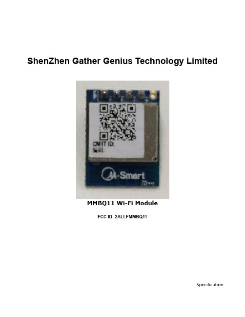
ShenZhen Gather Genius Technology LimitedMMBQ11 Wi-Fi ModuleFCC ID: 2ALLFMMBQ11SpecificationMMBQ11 WIFI Module DatasheetVersion 1.1 Disclaimer and noticeThe document is provided “AS IS,”without warranty of any kinds, including the implied warranties of merchantability and applies to any guarantee for a particular purpose, or non infringement, and any proposal, specification or sample of any guarantee mentioned anywhere else.This document does not bear any responsibility, including the use of the document information from infringement of any patent infringement liability.This document is not here by estoppel or otherwise, any intellectual property rights is granted the license, whether express or implied license.The information in this document might be modified for upgrade or other reasons.ShenZhen Gather Genius Technology Limite reserves the rights to make change withoutnotice. This document is used for design guide only, ShenZhen Gather Genius Technology Limitedtry the best to supply the correct information, but it does not assure there is not any error in this document. All the ostensive or implied states, information, suggestion are not guaranteed.INDEX1.GENERAL DESCRIPTION (2)1.1.Features (2)2.Pin assignment (4)3.Package and dimensions (5)4.Main function description (6)4.1.MCU (6)4.2.Memory (6)4.3.Interface (6)4.4.Absolute maximum ratings (6)4.5.Recommended operating range (7)5.RF specification (7)6.Power consumption (8)7.Recommended Reflow Profile (8)8.AT instruction (10)8.1.General AT instruction description (10)8.2.Operation instruction description (11)8.3.TCP/UDP port (14)8.4.GPIO/PWM instructions description (16)8.5.SMART LINK instruction description (17)8.6.SOFT AP instructions description (17)8.7.RF instructions description (18)8.8.Other description (23)1.GENERAL DESCRIPTIONThe MMBQ11module supports standard IEEE802.11 b/g/n protocol, TCP/IP stack and support STA, AP, STA+AP work mode. It can be used in the present device for additional Wi-Fi feature, or to design standalone network controller.MMBQ11 is a total solution for Wi-Fi network, which can be used separately.It can boot from external flash directly and designed to work with external MCU.In this case, MMBQ11can be added to any micro-controller system through UART interface.MMBQ11 is highly integrated with antenna switch, BALUN, PA, PMU. It just needs a few components for external circuit, which help to save the PCB room and cost furthest.1.1.Features•Support 802.11 b/g/n;•Embedded TCP/IP protocol stack;•Integrated TR switch/Balun/LNA/PA/antenna;•MCU clock frequency up to 160M, internal cache 8kB;•Integrated 16Mbitsflash;•Supply voltage range: 4.75V~5.25VDC, single 5V is recommended to use.•Support OTA firmware upgrade, which can be initiated with mobile phone APP and AT command;•Support STA, AP ,AP+STA mode;•Support Smart Link;•Support WEP/TKIP/WPA/WPA2 protocol;•Support802.11e and WMM/WMM PS;•Support UART;•Support HT20/40;Table 1 Major hardware and software features2.Pin assignmentThere are 4pins in MMBQ11 module, Figure1 is the pin assignment, Table 2 is the pin definition.Figure 1MMBQ11 pin assignmentTable 2 MMBQ11 pin definition3.Package and dimensionsThe dimensions of MMBQ11 module is 15mm*20mm*9.5mm(Figure 3), and it integrates 16Mb SPI Flash and 0 dBi PCB antenna.Figure 2MMBQ11module exteriorFigure 3MMBQ11 module dimensions4.Main function description4.1.MCUThe MCU of MMBQ11 is a low-power single chip, it supply integrated solution for embedded smart family system. It integrated 2.4 GHz WLAN CMOS PA and LNA. The RF front-end is single-ended double-direction. Also, it integrates LDO and DC-DC converter, which can separate digital circuit and analog circuit for lower noise.4.2.Memory4.2.1. Built- in SRAMMMBQ11 integrates 192KB SRAM。
PS21867-P中文资料

Powerex, Inc., 200 E. Hillis Street, Youngwood, Pennsylvania 15697-1800 (724) 925-7272Intellimod™ ModuleDual-In-Line Intelligent Power Module30 Amperes/600 VoltsPS21867-P1Description:DIP-IPMs are intelligent power modules that integrate power devices, drivers, and protection circuitry in an ultra compactdual-in-line transfer-mold package for use in driving small three phase motors. Use of 5thgeneration IGBTs, DIP packaging, and application specific HVICs allow the designer to reduce inverter size and overall design time.Features:£ Compact Packages £ Single Power Supply £ Integrated HVICs£ Direct Connection to CPU Applications:£ Washing Machines £ Refrigerators £ Air Conditioners £ Small Servo Motors £ Small Motor ControlOrdering Information:PS21867-P is a 600V , 30 Ampere DIP Intelligent Power Module.Dimensions Inches Millimeters A 3.11±0.02 79.0±0.5 B 1.22±0.02 31.0±0.5 C 0.28±0.02 7.0±0.5 D 2.64±0.01 67.0±0.3 E 0.53±0.02 13.4±0.5 F 0.84±0.02 21.4±0.5 G 1.37±0.02 34.9±0.5 H 0.15±0.01 3.8±0.2 J 0.11±0.01 2.8±0.3 K 0.39±0.01 10.0±0.3 L 0.79±0.01 20.0±0.3 M 0.50±0.04 12.8±1.0 N 2.98 75.6P0.041.0Dimensions Inches Millimeters Q 0.18±0.01 Dia. 4.5±0.2 Dia. R 0.07±0.002 1.9±0.05 S 0.04±0.01 1.0±0.2 T 0.02 Max. 0.5 Max. U 0.06±0.02 1.6±0.5 V 0.07±0.002 1.70±0.05 W 0.03±0.01 0.8±0.2 X 0.45±0.02 11.5±0.5 Y 0.13 Max. 3.25 Max.Z 0.03 0.7 AA 0.18 4.5 BB 0.12 3.1 CC 0.02 0.6DD0.07 Max.1.85 Max.Powerex, Inc., 200 E. Hillis Street, Youngwood, Pennsylvania 15697-1800 (724) 925-7272PS21867-PIntellimod™ ModuleDual-In-Line Intelligent Power Module30 Amperes/600 VoltsAbsolute Maximum Ratings, T j = 25°C unless otherwise specifiedCharacteristics Symbol PS21867-P Units Power Device Junction Temperature* T j-20 to 125 °C Module Case Operation T emperature (See T f Measurement Point Illustration) T f-20 to 100 °C Storage Temperature T stg-40 to 125 °C Mounting Torque, M4 Mounting Screws — 13 in-lb Module Weight (Typical) — 65 Grams Self-protection Supply Voltage Limit (Short Circuit Protection Capability)** V CC(prot.)400 Volts Isolation Voltage, AC 1 minute, 60Hz Sinusoidal, Connection Pins to Heatsink Plate V ISO2500 Volts *The maximum junction temperature rating of the power chips integrated within the DIP-IPM is 150°C (@T f≤ 100°C). However, to ensure safe operation of the DIP-IPM,the average junction temperature should be limited to T j(avg)≤ 125°C (@T f≤ 100°C).**V D = 13.5 ~ 16.5V, Inverter Part, T j = 125°C, Non-repetitive, Less than 2µsIGBT Inverter SectorCollector-Emitter Voltage (T f = 25°C) V CES600 Volts Collector Current (T f = 25°C) ±I C30 Amperes Peak Collector Current (T f = 25°C, <1ms) ±I CP60 Amperes Supply Voltage (Applied between P - N) V CC450 Volts Supply Voltage, Surge (Applied between P - N) V CC(surge)500 Volts Collector Dissipation (T f = 25°C, per 1 Chip) P C60.6 WattsControl SectorSupply Voltage (Applied between V P1-V PC, V N1-V NC) V D20 Volts Supply Voltage (Applied between V UFB-V UFS,V VFB-V VFS, V WFB-V WFS) V DB20 Volts Input Voltage (Applied between U P, V P, W P-V PC, U N, V N, W N-V NC) V IN-0.5 ~ V D+0.5 Volts Fault Output Supply Voltage (Applied between F O-V NC) V FO-0.5 ~ V D+0.5 Volts Fault Output Current (Sink Current at F O Terminal) I FO 1 mA Current Sensing Input Voltage (Applied between C IN-V NC) V SC-0.5 ~ V D+0.5 Volts2Powerex, Inc., 200 E. Hillis Street, Youngwood, Pennsylvania 15697-1800 (724) 925-7272PS21867-PIntellimod™ ModuleDual-In-Line Intelligent Power Module30 Amperes/600 VoltsElectrical and Mechanical Characteristics, T j = 25°C unless otherwise specifiedCharacteristics Symbol Test Conditions Min. Typ. Max. UnitsIGBT Inverter SectorCollector-Emitter Cutoff Current I CES V CE = V CES, T j = 25°C — — 1.0 mAV CE = V CES, T j = 125°C — — 10 mA Diode Forward Voltage V EC T j = 25°C, -I C = 30A, V IN = 5V — 1.5 2.0 Volts Collector-Emitter Saturation Voltage V CE(sat)I C = 30A, T j = 25°C, V D = V DB = 15V, V IN = 0V — 1.6 2.1 VoltsI C = 30A, T j = 125°C, V D = V DB = 15V, V IN = 0V — 1.7 2.2 Volts Inductive Load Switching Times t on0.7 1.30 1.90 µsrr CC D DBC(on)C j INoffC(off)T fMeasurement Point3Powerex, Inc., 200 E. Hillis Street, Youngwood, Pennsylvania 15697-1800 (724) 925-7272PS21867-PIntellimod™ ModuleDual-In-Line Intelligent Power Module30 Amperes/600 VoltsElectrical and Mechanical Characteristics, T j = 25°C unless otherwise specifiedCharacteristics Symbol Test Conditions Min. Typ. Max. UnitsControl SectorSupply Voltage V D Applied between V P1-V PC, V N1-V NC13.5 15.0 16.5 VoltsV DB Applied between V UFB-V UFS, 13.0 15.0 18.5 VoltsV VFB-V VFS, V WFB-V WFSCircuit Current I D V D = V DB = 15V, V IN = 5V, — — 5.00 mATotal of V P1-V PC, V N1-V NCV D = V DB = 15V, V IN = 0V, — — 7.00 mATotal of V P1-V PC, V N1-V NCV D = V DB = 15V, V IN = 5V, — — 0.40 mAV UFB-V UFS, V VFB-V VFS, V WFB-V WFSV D = V DB = 15V, V IN = 0V, — — 0.55 mAV UFB-V UFS, V VFB-V VFS, V WFB-V WFSFault Output Voltage V FOH V SC = 0V, F O Circuit: 10kΩ to 5V Pull-up 4.9 — — VoltsV FOL V SC = 1V, I FO = 1mA — — 0.95 Volts Input Current I IN V IN = 5V 1.0 1.50 2.00 mA Short-Circuit Trip Level* V SC(ref)T j = 25°C, V D = 15V 0.43 0.48 0.53 Volts Supply Circuit Undervoltage UV DBt T rip Level, T j≤ 125°C 10.0 — 12.0 Volts Protection UV DBr Reset Level, T j≤ 125°C 10.5 — 12.5 VoltsUV Dt Trip Level, T j≤ 125°C 10.3 — 12.5 VoltsUV Dr Reset Level, T j≤ 125°C 10.8 — 13.0 Volts Fault Output Pulse Width** t FO C FO = 22nF 1.0 1.8 — msth(on)P P P PC,Thermal CharacteristicsCharacteristic Symbol Condition Min. Typ. Max. Units Junction to Fin R th(j-f)Q IGBT Part (Per 1/6 Module) — — 1.65 °C/Watt Thermal Resistance R th(j-f)D FWDi Part (Per 1/6 Module) — — 3.00 °C/Watt * Short-Circuit protection is functioning only at the lower arms. Please select the value of the external shunt resistor such that the SC trip level is less than 51A.**Fault signal is asserted when the lower arm short circuit or control supply under-voltage protective functions operate. The fault output pulse-width t FO depends on the capacitance value of C FO according to the following approximate equation: C FO = (12.2 x 10⁻⁶) x t FO {F} .45PS21867-PIntellimod™ ModuleDual-In-Line Intelligent Power Module 30 Amperes/600 VoltsPowerex, Inc., 200 E. Hillis Street, Youngwood, Pennsylvania 15697-1800 (724) 925-7272Recommended Conditions for UseCharacteristic Symbol ConditionMin. Typ. Value Units Supply Voltage V CC Applied between P-N T erminals 0 300 400 Volts Control Supply Voltage V D Applied between V P1-V PC , V N1-V NC13.5 15.0 16.5 Volts V DB Applied between V UFB -V UFS , 13.015.018.5VoltsV VFB -V VFS , V WFB -V WFSControl Supply Variation ΔV D , ΔV DB-1 — 1 V/µs PWM Input Frequency f PWM T f ≤ 100°C, T j ≤ 125°C — 5 — kHz Allowable rms Current* I O V CC = 300V , V D = 15V , f C = 5kHz, — — 18.9 Arms PF = 0.8, Sinusoidal, T j ≤ 125°C, T f ≤ 100°CV CC = 300V , V D = 15V , f C = 15kHz, — — 11.6 ArmsPF = 0.8, Sinusoidal, T j ≤ 125°C, T f ≤ 100°CMinimum Input Pulse Width** P WIN ON / OFF300 — — ns V NC VariationV NC Between V NC -N (Including Surge) -5.0 — 5.0 Volts Arm Shoot-through Blocking Timet DEADFor Each Input Signal, T f < 100°C2.0——µs* The allowable rms current value depends on the actual application conditions.**The input pulse width less than P WIN might make no response.REVERSE RECOVERY CHARACTERISTICS(TYPICAL)100102101EMITTER CURRENT, I E , (AMPERES)R E V E R S E R E C O V E R Y T I M E , t r r , (n s )100102101COLLECTOR CURRENT, I C , (AMPERES)103100102101102101COLLECTOR CURRENT, I C , (AMPERES)C O L L E C T O R -E M I T T E R S A T U R A T I O N V O L T A G E , V C E (s a t ), (V O L T S )COLLECTOR-EMITTERSATURATION VOLTAGE CHARACTERISTICS(TYPICAL)FREE-WHEEL DIODEFORWARD CHARACTERISTICS(TYPICAL)3.02.52.01.51.00.50Powerex, Inc., 200 E. Hillis Street, Youngwood, Pennsylvania 15697-1800 (724) 925-7272PS21867-PIntellimod™ ModuleDual-In-Line Intelligent Power Module30 Amperes/600 VoltsDIP-IPM Application Circuit (Shown Pins Up)plane.Component Selection:Dsgn.T yp. Value DescriptionD11A, 600V Boot strap supply diode – Ultra fast recoveryC110-100uF, 50V Boot strap supply reservoir – Electrolytic, long life, low Impedance, 105°C (Note 5)C20.22-2.0uF, 50V Local decoupling/High frequency noise filters – Multilayer ceramic (Note 8)C310-100uF, 50V Control power supply filter – Electrolytic, long life, low Impedance, 105°CC422nF, 50V Fault lock-out timing capacitor – Multilayer ceramic (Note 4)C5100pF, 50V Optional input signal noise filter – Multilayer ceramic (Note 1)C6200-2000uF, 450V Main DC bus filter capacitor – Electrolytic, long life, high ripple current, 105°CC70.1-0.22uF, 450V Surge voltage suppression capacitor – Polyester/Polypropylene film (Note 9)C SF1000pF, 50V Short circuit detection filter capacitor – Multilayer Ceramic (Note 6, Note 7)R SF 1.8k ohm Short circuit detection filter resistor (Note 6, Note 7)R SHUNT5-100 mohm Current sensing resistor - Non-inductive, temperature stable, tight tolerance (Note 10)R110 ohm Boot strap supply inrush limiting resistor (Note 5)R2330 ohm Optional control input noise filter (Note 1, Note 2)R310k ohm Fault output signal pull-up resistor (Note 3)Notes:1) T o prevent input signal oscillations minimize wiring length to controller (~2cm). Additional RC filtering (C5 etc.) may berequired. If filtering is added be careful to maintain proper dead time. See application notes for details.2) Internal HVIC provides high voltage level shifting allowing direct connection of all six driving signals to the controller.3) F O output is an open collector type. Pull up resistor (R3) should be adjusted to current sink capability of the module.4) C4 sets the fault output duration and lock-out time. C4 12.2E-6 x t FO, 22nF gives ~1.8ms5) Boot strap supply component values must be adjusted depending on the PWM frequency and technique.6) Wiring length associated with R SHUNT, R SF, C SF must be minimized to avoid improper operation of the SC function.7) R SF, C SF set short-circuit protection trip time. Recommend time constant is 1.5us-2.0us. See application notes.8) Local decoupling/high frequency filter capacitors must be connected as close as possible to the modules pins.9) The length of the DC link wiring between C6, C7, the DIP’s P terminal and the shunt must be minimized to preventexcessive transient voltages. In particular C7 should be mounted as close to the DIP as possible.10) Use high quality, tight tolorance current sensing resistor. Connect resistor as close as possible to the DIP’sN terminal. Be careful to check for proper power rating. See application notes for calculation of resistance value.6。
LB1836M-TLM-E;中文规格书,Datasheet资料

Monolithic Digital ICLow-Saturation Bidirectional Motor Driver for Low-Voltage DriveLB1836MOverviewThe LB1836M is a low-saturation two-channel bidirectional motor driver IC for use in low-voltage applications. The LB1836M is a bipolar stepper-motor driver IC that is ideal for use in printers, FDDs, cameras and other portable devices.Features• Low voltage operation (2.5V min)• Low saturation voltage (upper transistor + lower transistor residual voltage ; 0.40V typ at 400mA). • Parallel connection (Upper transistor + lower transistor residual voltage ; 0.5V typ at 800mA). • Separate logic power supply and motor power supply • Brake function• Spark killer diodes built in• Thermal shutdown circuit built in • Compact package (14-pin MFP)SpecificationsAbsolute Maximum Ratings at Ta = 25°CParameter SymbolConditionsRatingsUnitV CC max -0.3 to +10.5V Maximum supply voltageV S max-0.3 to +10.5V Output supply voltage V OUT V S + V SF V Input supply voltageV IN-0.3 to +10VGND pin flow-out current IGND Per channel 1.0 A Allowable power dissipation Pd max * Mounted on a board. 800mW Operating temperature Topr -40 to +85°C Storage temperatureTstg-55 to +150°C* Mounted on a substrate: 30×30×1.5mm 3, glass epoxy board.Allowable Operating Ranges at Ta = 25°CParameter SymbolConditionsRatingsUnit V CC 2.5 to 9.0V Supply voltageV S1.8 to 9.0V Input “H”-level voltage V IH 1.8 to 9.0V Input “L”-level voltageV IL-0.3 to +0.7VElectrical Characteristics at Ta = 25°C, V CC = VS = 3VRatingsParameter SymbolConditionsmin typ maxUnitI CC 0 V IN 1, 2, 3, 4 = 0V, I CC + I S 0.1 10μAI CC 1 V IN 1 = 3V, V IN 2, 3, 4 = 0V, I CC + I S 14 20mASupply currentI CC 2 V IN 1, 2 = 3V, V IN 3, 4 = 0V, I CC + I S 2235mA V OUT 1 I OUT = 200mA 0.20 0.28V V OUT 2 I OUT = 400mA0.40 0.60V V OUT 3 I OUT = 400mA, Parallel connection 0.25 0.35V Output saturation voltage (upper + lower)V OUT 4 I OUT = 800mA, Parallel connection0.500.70V Output sustain voltage V O (SUS)I OUT = 400mA 9V Input current I INV IN = 2V, V CC = 6V80μASpark killer diode Reverse current I S (leak) V CC 1, 2 = 9V 30μA Forward voltageV SFI OUT = 400mA1.7VPackage Dimensionsunit : mm (typ) 3111A Ambient temperature, Ta -- °CA l l o w a b l e p o w e r d i s s i p a t i o n , P d m a x -- m WPin Assignment 14GND 1V CC 13IN32IN112OUT33OUT111VS24VS110OUT45OUT29IN46IN28Vcont 7GNDLB1836MTop viewNote) Ground both GND pins.Block DiagramIN1IN2IN3IN4Truth TableOUT2/4 Mode IN1/3 IN2/4 OUT1/3ForwardH L H LReverse L H L HH H L L BrakeStandby L L OFFOFFDesign NotesIf large current flows on the power supply (V S) line and the GND line, then in some applications and layouts, misoperation due to line oscillation may result.The modes during which large current flows are as follows :• Motor surge current when the DC motor starts up or when it shifts rotation directions (forward ↔ reverse).• Passthrough current generated within the IC when shifting rotation directions (forward ↔ reverse) or when shifting from forward/reverse rotation to braking, or vice versa.The following points should be kept in mind regarding the pattern layout :• Keep the wiring lines thick and short in order to reduce wiring inductance between the power supply (V S) and GND. • Insert a passthrough capacitor near the IC. (Maximum effect is obtained by inserting the passthrough capacitor between VS and the pin 7 GND at the closest distance possible.• If the CPU and the LB1836M are mounted on separate boards and the difference between the ground potential of each board is large, install resistors of about 10kΩ in series between the CPU and the LB1836M inputs.Vcont pinAs shown in the above diagram, the Vcont pin outputs the voltage of the band gap Zener V Z + V F (=1.93V).In normal use, this pin is left open.The drive current ID is varied by the Vcont voltage. However, because the band gap Zener is shared, it functions as a bridge.0.20.40.60.81.00200100300400500600Output current, I O –mAO u t p u t s a t u r a t i o n v o l t a g e , V O Ambient temperature, Ta –°CO Ambient temperature, Ta –°CS Ambient temperature, Ta –°CC u r r e n t d r a i n , I C C –m ASupply voltage, V CC –VC u r r e n t d r a i n , I C C –m AOutput current, I O –mAO u t p u t s a t u r a t i o n v o l t a g e , V O (s a t )–VAmbient temperature, Ta –°CI n p u t c u r r e n t , I I N –μAV O (sat) – I OInput voltage, V IN –V I N V– (s a t )–V(s a t )O u t p u t s a t u r a t i o n v o l t a g e , V –m AC u r r e n t d r a i n , I –μAI n p u t c u r r e n t , ISupply voltage, V S –VThis catalog provides information as of January, 2007. Specifications and information herein are subject This catalog provides information as of March, 2010. Specifications and information herein are subject to change without notice.C u r r e n t d r a i n , I S –m A分销商库存信息: ONSEMILB1836M-TLM-E。
艾тон电子变频驱动器产品介绍说明书

V/Hz Energy Savings Percentage
Eaton - Active Energy Control Competitor 1 Competitor 2 Competitor 3
35
40
45
50
55
Frequency (Hz)
• Active Energy Control - minimizes energy losses in your motor by dynamically adjusting V/Hz curve to optimize efficiency
• Compare Functionality • PC Control Online Operate
Mode
© 2013 Eaton Corporation. All rights reserved.
13
Energy Saving Functionality
Percentage
10.0% 8.0% 6.0% 4.0% 2.0% 0.0% -2.0% 30 -4.0%
• Easy to Use PC Based Drive Software Configuration Tool
• Provides Parameter Description, Min, Max, and Default Values
• Monitoring and Data Logging Capabilities
© 2013 Eaton Corporation. All rights reserved.
Electrical Wholesalers
End Users Maintenance, Repair, and Operations (MRO) Opportunities
viliv S5 用户手册说明书

ContentsSafety Precautions for Use (4)Names of Parts (7)Basic Components (7)Front View (8)Top View (9)Left/Right View (10)Rear View (11)Installation and Cable Connection (12)USB Data Link Connection (12)USB Connection (12)Separating.Attaching Battery (13)Separating Battery (13)Attaching Battery (13)Inserting.Extracting USIM Card (14)Basic Operation (15)Power On/Off (15)Setting/Cancelling Hold Function (15)Volume Control (16)Mute (16)Resetting (16)Jog and Function Buttons (17)Turning On/Off the LCD Screen (18)Touch Screen (18)Virtual Keyboard (18)Set Up for villv Manager (19)Using for the First Time (20)Using for the First Time (20)Recovery Solution (AMI Rescue) Guide (22)Way to Use Recovery Solution (AMI Rescue) (22)Specifications (23)General Specifications (23)Information to UserThis equipment has been tested and found to comply with the limits for a Class B digital device, pursuant to part15 of the FCC Rules. These limits are designed to provide reasonable protection against harmful interference in a residential installation. This equipment generates, uses and can radiate radio frequency energy and, if not installed and used in accordance with the instructions, may cause harmful interference to radio communications. However, there is no guarantee that interference will not occur in a particular installation. If this equipment does cause harmful interference to radio or television reception, which can be determined by turning the equipment off and on, the user is encouraged to try to correct the interference by one or more of the following measures:- Reorient or relocate the receiving antenna.- Increase the separation between the equipment and receiver.- Connect the equipment into an outlet on a circuit different from that to which the receiver is connected.- Consult the dealer or an experienced radio/ tv technician for help.FCC RF Exposure InformationIn August 1996 the Federal Communications Commission(FCC) of the United States with its action in Report and order 96-326 adopted an updated safety standard for human exposure the ra-dio frequency electromagnetic energy emitted by FCC regulated transmitters. Those guidelines are consistent with the safety standard previously set by both U.S. and international standards bodies. The design of ‘S5’ complies with the FCC guidelines and those international standards. Use only the supplied or an approved antenna. Unauthorized antennas, modifications, or attachments could impair call quality, damage your ‘S5’, or result in violation of FCC regulations.‘S5’ was tested for typical body-wom operation using the optional belt-clip / holster placed touch(0cm) from the body. The use of non-tested accessories or other body-wom operations may not comply with FCC exposure requirements and should be avoided.Rear ViewThe figure below shows the rear side of the main body without the battery. (Refer to Page 13 for Separating/Attaching battery.)USB ConnectionSeparating BatteryInserting · Extracting USIM CardHow to Insert : L et the front of a USIM card face the USIM card slot and then push it in the arrow direction until a click sound is heard. (If, however, you push the USIMcard using too much force, the card may be damaged.)How to Extract : S ince this device adopts a one-touch method, you may gently press on the end of the USIM card to extract it automatically. (Pull out the USIM cardslightly protruded.)Power On/OffSetting/Cancelling Hold FunctionVolume ControlMuteResettingUse the Reset button if the touch screen and/or the buttons on the device do not work.Jog and Function ButtonsThe Jog key has different functions in accordance with the program functions.Turning On/Off the LCD ScreenTouch ScreenVirtual KeyboardRight-click the icon on the task bar and selectSet Up for villv Managerviliv Manager is executed by double touching vilivManager on the screen.1Wireless LAN Power Turn on/off self-powered wireless LAN function.2Bluetooth Power Turn on/off self-powered Bluetooth function.33G Modem Power (3G Model only)Turn on/off self-powered 3G Modem function.4Windows Start Option 1. OFF: Always start with OFF status.2. Last Status: Start with the last status.3. ON: Always start with ON status.5Brightness of LCD Adjust by status bar or -, + button.6Setting Vibration 1. No Use: Do not use vibration function.2. When using soft keyboard: O perate only if softkeyboard is used.3. Always Use: O perates when operating for alltouches.7Set Up for Windows Start Program 1. Set whether or not to execute Cube UI automatically.2. S et whether or not to execute viliv Managerautomatically.1423567Using for the First TimeFor each Windows installation process, the installation time may vary depending on the process. Please wait until the installation is complete.It may take a couple of minutes. Please wait for a moment.Way to Use Recovery Solution (AMI Rescue)General Specifications。
无刷电机解决方案

Level Shift
OUT1 (NC) (NC) VCC
5 6 7 8
Current Limitter
Duty Controller
12 11 10
High Side Regulator
RD FG PWM
OSC Lock Detection
PWM
RGH
9
TSD
订购及封装信息
ONPN Description LV8861VH-TLM-H FAN MOTOR DRIVER (7.6mmx9.75mmx1.3mm) Pkg HSSOP16
ON Semiconductor Target
19
LB1975/76
三相风扇电机驱动器
独特特性 • 3-Phase Bipolar Drive VMmax46V,Iomax2.5A VMmax60V,Iomax2.5A • Direct PWM Drive • DIP28H Package 优势 应用数据 • High voltage,current 1chip • LB1975 VREG • LB1976 VCC • High Efficiency Reg VCC • Large Power dissipation
+
S/S
F/R
FG1 FG2
LVSD
TSD VM
+
Hys.Amp
VM
• • • •
其它特性 Built-in high side kickback absorbing diodes Built-in current limiter Built-in FG output PWM duty can be controlled by IC input
控制器
- 1、下载文档前请自行甄别文档内容的完整性,平台不提供额外的编辑、内容补充、找答案等附加服务。
- 2、"仅部分预览"的文档,不可在线预览部分如存在完整性等问题,可反馈申请退款(可完整预览的文档不适用该条件!)。
- 3、如文档侵犯您的权益,请联系客服反馈,我们会尽快为您处理(人工客服工作时间:9:00-18:30)。
During drive During lock protection I5VREG = 5mA
VCPWM = 0.5V VCPWM = 3.5V C = 220PF
VCT = 0.5V VCT = 3.5V ICT1/ICT2 VS-S = 1V IO = 10mA IO = 10mA IO = 10mA IN+, IN- differential voltage (including offset and hysteresis) IFG = 5mA VFG = 19V CPWM = VTH/RMI = 2V
• Variable speed control possible with external PWM input ⇒ Separately-excited upper direct PWM (f =30kHz) control method ensures highly silent speed control.
VS-S max VFG max IFG max I5VREG max
Pd max
with specified substrate *1
Operating temperature
Topr
*2
Storage temperature
Tstg
*1 Specified substrate: 114.3mm×76.1mm×1.6mm, glass epoxy board. *2 Tj max=150°C must not be exceeded.
FG output L-level voltage FG pin leakage current VTH/RMI pin bias current
ICC1 ICC2 5VREG VLIM VCPWMH VCPWML ICPWM1 ICPWM2 FPWM VCTH VCTL ICT1 ICT2 RCT IS-S VONH VONL VOPL VHN
• Current limiting circuit incorporated ⇒ Chopper type current limiting made at startup and during lock.
• Reactive current cut circuit incorporated ⇒ Reactive current before phase changeover is cut, ensuring highly silent and low power-consumption drive.
Ordering number : ENA0730B
LB11867FV
Monolithic Digital IC
For Fan Motor
Variable Speed Single-phase Full-wave Pre-driver
Overview
LB11867FV is a single-phase bipolar driving motor pre-driver with the variable speed function compatible with external PWM signal. With a few external parts, a highly-efficient and highly-silent variable drive fan motor with low power consumption can be achieved. This product is best suited for driving of the server requiring large air flow and large current and the fan motor of consumer appliances.
Symbol VCC max IOUTN max
IOUTP max
Conditions
OUT pin output withstand voltage
VOUT max
VTH, RMI pins withstand voltage VVTH, VRMI max
S-S pin withstand voltage FG output pin withstand voltage FG pin maximum output current 5VREG pin maximum output current Allowable power dissipation
Features
• Single-phase full-wave driving pre-driver ⇒ Low-saturation drive using external PMOS-NMOS enables high-efficiency low power-consumption drive.
• Minimum speed setting pin ⇒ Minimum speed can be set by setting the resistance.
• Soft start setting pin • Lock protection and automatic reset circuits incorporated • FG (rotation speed detection) output • Thermal shutdown circuit incorporated
Ratings
Unit
18
V
20
mA
20
mA
18
V
7
V
7
V
19
V
10
mA
20
mA
800 mW
-30 to 95
°C
-55 to 150
°C
Ratings
Unit
5.5 to 16
V
0 to 5
/
11911 SY/O1007 MS/50907 MS PC 20070228-S00004 No.A0730-1/9
பைடு நூலகம்
LB11867FV
Specifications
Absolute Maximum Ratings at Ta = 25°C
Parameter VCC pin maximum supply voltage OUTN pin maximum output current OUTP pin maximum Sink current
Recommended Operating Conditions at Ta = 25°C
Parameter VCC Supply voltage VTH, RMI input voltage range Hall input common-phase input voltage range
Symbol VCC
Specifications of any and all SANYO Semiconductor Co.,Ltd. products described or contained herein stipulate the performance, characteristics, and functions of the described products in the independent state, and are not guarantees of the performance, characteristics, and functions of the described products as mounted in the customer's products or equipment. To verify symptoms and states that cannot be evaluated in an independent device, the customer should always evaluate and test devices mounted in the customer's products or equipment.
Any and all SANYO Semiconductor Co.,Ltd. products described or contained herein are, with regard to "standard application", intended for the use as general electronics equipment (home appliances, AV equipment, communication device, office equipment, industrial equipment etc.). The products mentioned herein shall not be intended for use for any "special application" (medical equipment whose purpose is to sustain life, aerospace instrument, nuclear control device, burning appliances, transportation machine, traffic signal system, safety equipment etc.) that shall require extremely high level of reliability and can directly threaten human lives in case of failure or malfunction of the product or may cause harm to human bodies, nor shall they grant any guarantee thereof. If you should intend to use our products for applications outside the standard applications of our customer who is considering such use and/or outside the scope of our intended standard applications, please consult with us prior to the intended use. If there is no consultation or inquiry before the intended use, our customer shall be solely responsible for the use.