笙泉8051单片机选型表
C8051F单片机选型列表

200 ksps
32引
-
√ √ 2 - 脚,
9x9,
LQFP
28引
-
√ √ 2 - 脚,
5x5,
QFN
48引
-
√ √ 2 - 脚,
9x9,
TQFP
/Left_Column/detail/C8051F_51_Device.asp
1/31/2013
C8051F 51 单片机 选型列表
Page 1 of 3
C8051F 51 单片机 选型列表
Precision Mixed-Signal
型号 C8051F005 C8051F007 C8051F020 C8051F021 C8051F022 C8051F023 C8051F040 C8051F060
C8051F 51 单片机 选型列表
Page 3 of 3
C8051F410 50 32 kB 2304 -
UART, 24 SMBus, 4
SPI
6
±2%
12位, 24通 道,
-
32引
12位, √ 2通道
√
2
VREG, 脚, smaRTClock 9x9,
200
LQFP
ksps
USB MCUs
型号 C8051F320 C8051F321 C8051F340
100引
-
脚,
16x16,
TQFP
10位, 8位, ±20% 8通道, 8通道, 12位, √ √ 2
100 500 2通道
ksps ksps
64引
-
脚,
12x12,
TQFP
±2%
12位, 13通 道,
ATMEL 单片机选型指南
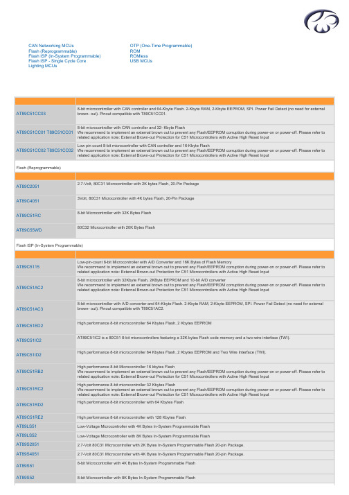
Flash ISP (In-System Programmable)
芯片型号
描述
AT89C5115
Low-pin-count 8-bit Microcontroller with A/D Converter and 16K Bytes of Flash Memory We recommend to implement an external brown out to prevent any Flash/EEPROM corruption during power-on or power-off. Please refer to related application note: External Brown-out Protection for C51 Microcontrollers with Active High Reset Input
High performance 8-bit Microcontroller 16 kbytes Flash We recommend to implement an external brown out to prevent any Flash/EEPROM corruption during power-on or power-off. Please refer to related application note: External Brown-out Protection for C51 Microcontrollers with Active High Reset Input High performance 8-bit microcontroller 32 Kbytes Flash We recommend to implement an external brown out to prevent any Flash/EEPROM corruption during power-on or power-off. Please refer to related application note: External Brown-out Protection for C51 Microcontrollers with Active High Reset Input High performance 8-bit microcontroller with 64 Kbytes Flash
台湾笙泉8051系列单片机选型表 20130627
4.5V~5.5V 2.4V~3.6V
64KB 256B+1024B
3 37 / 41
10bit , 8-CH 无
MA807
4.5V~5.5V
16KB
3
MA808
2.4V~3.6V
256B+256B
41
24MHz *2
MA816
4.5V~5.5V
16KB
3
256B+256B
57
无
x1
UART
无
x1
MA82G5A64 *0 2.0V~5.5V
封装
PDIP 20 / 16 / 8 SOP 20 / 16 / 8
SOP 28 / 20
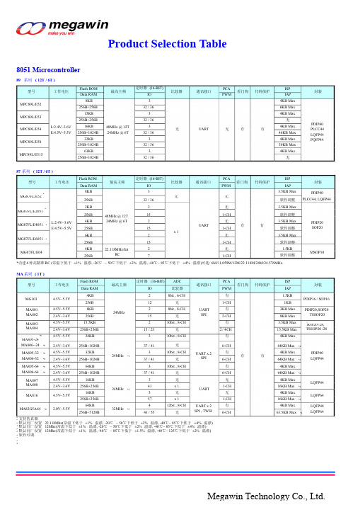
20 系列( 1T , MTP )
型号 MA20E/L809
工作电压
L:2.4V~3.6V E:4.5V~5.5V
Flash ROM Data RAM
4KB 256B+128B
最高主频 25MHz *1
定时器 (16-BIT) IO
*5
软件可调
ISP
IAP
4KB Max
15KB Max
4KB Max
15KB Max
4KB Max
63KB
*5
Max
封装
LQFP48
LQFP48 LQFP64
Low-Speed USB Microcontroller
64 系列 ( 6502 , USB LS )
型号
工作电压
MG64F236 *使用内置晶振
FAX:86-755-82877039 / 82877063
FAX:86-21-54314771
Atmel 8051 微控制器家族 - 产品选择指南.pdf_1702133939.8143017说

Continued....Features Array•Compatible with MCS-51™ Products•4K Bytes of Reprogrammable Flash Memory–Endurance: 1,000 Write/Erase Cycles• 3.0V to 6V Operating Range•Fully Static Operation: 0 Hz to 24 MHz•Two-Level Program Memory Lock•128 x 8-Bit Internal RAM•15 Programmable I/O Lines•Two 16-Bit Timer/Counters•Six Interrupt Sources•Programmable Serial UART Channel•Direct LED Drive Outputs•On-Chip Analog Comparator•Low Power Idle and Power Down Modes•Brown-Out DetectionDescriptionThe AT89C4051 is a low-voltage, high-performance CMOS 8-bit microcomputer with 4K Bytes of Flash programmable and erasable read only memory (PEROM). The device is manufactured using Atmel’s high density nonvolatile memory technology and is compatible with the industry standard MCS-51™ instruction set. By combining a versatile 8-bit CPU with Flash on a monolithic chip, the Atmel AT89C4051 is a pow-erful microcomputer which provides a highly flexible and cost effective solution to many embedded control applications.The AT89C4051 provides the following standard features: 4K Bytes of Flash, 128 bytes of RAM, 15 I/O lines, two 16-bit timer/counters, a five vector two-level interrupt architecture, a full duplex serial port, a precision analog comparator, on-chip oscillator and clock circuitry. In addition, the AT89C4051 is designed with static logic for opera-tion down to zero frequency and supports two software-selectable power saving modes. The Idle Mode stops the CPU while allowing the RAM, timer/counters, serial port and interrupt system to continue functioning. The Power Down Mode saves the RAM contents but freezes the oscillator disabling all other chip functions until the nexthardware reset.Block DiagramAT89C4051Pin DescriptionV CCSupply voltage.GNDGround.Port 1Port 1 is an 8-bit bidirectional I/O port. Port pins P1.2 to P1.7 provide internal pullups. P1.0 and P1.1 require exter-nal pullups. P1.0 and P1.1 also serve as the positive input (AIN0) and the negative input (AIN1), respectively, of the on-chip precision analog comparator. The Port 1 output buffers can sink 20 mA and can drive LED displays directly. When 1s are written to Port 1 pins, they can be used as inputs. When pins P1.2 to P1.7 are used as inputs and are externally pulled low, they will source current (I IL) because of the internal pullups.Port 1 also receives code data during Flash programming and verification.Port 3Port 3 pins P3.0 to P3.5, P3.7 are seven bidirectional I/O pins with internal pullups. P3.6 is hard-wired as an input to the output of the on-chip comparator and is not accessible as a general purpose I/O pin. The Port 3 output buffers can sink 20 mA. When 1s are written to Port 3 pins they are pulled high by the internal pullups and can be used as inputs. As inputs, Port 3 pins that are externally being pulled low will source current (I IL) because of the pullups. Port 3 also serves the functions of various special features of the AT89C4051 as listed below:Port 3 also receives some control signals for Flash pro-gramming and verification.RSTReset input. All I/O pins are reset to 1s as soon as RST goes high. Holding the RST pin high for two machine cycles while the oscillator is running resets the device.Each machine cycle takes 12 oscillator or clock cycles. XTAL1Input to the inverting oscillator amplifier and input to the internal clock operating circuit. XTAL2Output from the inverting oscillator amplifier.Oscillator CharacteristicsXTAL1 and XTAL2 are the input and output, respectively, of an inverting amplifier which can be configured for use as an on-chip oscillator, as shown in Figure 1. Either a quartz crystal or ceramic resonator may be used. To drive the device from an external clock source, XTAL2 should be left unconnected while XTAL1 is driven as shown in Figure 2. There are no requirements on the duty cycle of the external clock signal, since the input to the internal clocking circuitry is through a divide-by-two flip-flop, but minimum and maxi-mum voltage high and low time specifications must be observed.Figure 1. Oscillator ConnectionsNote:C1, C2= 30 pF ± 10 pF for Crystals= 40 pF ± 10 pF for Ceramic Resonators Figure 2. External Clock Drive ConfigurationPort Pin Alternate FunctionsP3.0RXD (serial input port)P3.1TXD (serial output port) P3.2INT0 (external interrupt 0) P3.3INT1 (external interrupt 1) P3.4T0 (timer 0 external input) P3.5T1 (timer 1 external input)Special Function RegistersA map of the on-chip memory area called the Special Func-tion Register (SFR) space is shown in the table below. Note that not all of the addresses are occupied, and unoc-cupied addresses may not be implemented on the chip. Read accesses to these addresses will in general return random data, and write accesses will have an indetermi-nate er software should not write 1s to these unlisted loca-tions, since they may be used in future products to invoke new features. In that case, the reset or inactive values of the new bits will always be 0.Table 1. AT89C4051 SFR Map and Reset Values0F8H0FFH0F0H B000000000F7H 0E8H0EFH0E0H ACC000000000E7H 0D8H0DFH0D0H PSW000000000D7H 0C8H0CFH 0C0H0C7H0B8H IPXXX000000BFH0B0H P3111111110B7H0A8H IE0XX000000AFH 0A0H0A7H98H SCON00000000SBUFXXXXXXXX9FH90H P11111111197H88H TCON00000000TMOD00000000TL000000000TL100000000TH000000000TH1000000008FH80H SP00000111DPL00000000DPH00000000PCON0XXX000087HAT89C4051Restrictions on Certain InstructionsThe AT89C4051 is an economical and cost-effective mem-ber of Atmel’s growing family of microcontrollers. It contains 4K bytes of flash program memory. It is fully compatible with the MCS-51 architecture, and can be programmed using the MCS-51 instruction set. However, there are a few considerations one must keep in mind when utilizing certain instructions to program this device.All the instructions related to jumping or branching should be restricted such that the destination address falls within the physical program memory space of the device, which is 4K for the AT89C4051. This should be the responsibility of the software programmer. For example, LJMP 0FE0H would be a valid instruction for the AT89C4051 (with 4K of memory), whereas LJMP 1000H would not.1. Branching instructions:LCALL, LJMP, ACALL, AJMP, SJMP, JMP @A+DPTR These unconditional branching instructions will execute correctly as long as the programmer keeps in mind that the destination branching address must fall within the physical boundaries of the program memory size (locations 00H to FFFH for the 89C4051). Violating the physical space limits may cause unknown program behavior.CJNE [...], DJNZ [...], JB, JNB, JC, JNC, JBC, JZ, JNZ With these conditional branching instructions the same rule above applies. Again, violating the memory boundaries may cause erratic execution.For applications involving interrupts the normal interrupt service routine address locations of the 80C51 family archi-tecture have been preserved.2. MOVX-related instructions, Data Memory:The AT89C4051 contains 128 bytes of internal data mem-ory. Thus, in the AT89C4051 the stack depth is limited to 128 bytes, the amount of available RAM. External DATA memory access is not supported in this device, nor is exter-nal PROGRAM memory execution. Therefore, no MOVX [...] instructions should be included in the program.A typical 80C51 assembler will still assemble instructions, even if they are written in violation of the restrictions men-tioned above. It is the responsibility of the controller user to know the physical features and limitations of the device being used and adjust the instructions used correspond-ingly.Program Memory Lock BitsOn the chip are two lock bits which can be left unpro-grammed (U) or can be programmed (P) to obtain the addi-tional features listed in the table below:Lock Bit Protection Modes(1)Note: 1.The Lock Bits can only be erased with the Chip Erase operation.Idle ModeIn idle mode, the CPU puts itself to sleep while all the on-chip peripherals remain active. The mode is invoked by software. The content of the on-chip RAM and all the spe-cial functions registers remain unchanged during this mode. The idle mode can be terminated by any enabled interrupt or by a hardware reset.P1.0 and P1.1 should be set to ’0’ if no external pullups are used, or set to ’1’ if external pullups are used.It should be noted that when idle is terminated by a hard-ware reset, the device normally resumes program execu-tion, from where it left off, up to two machine cycles before the internal reset algorithm takes control. On-chip hardware inhibits access to internal RAM in this event, but access to the port pins is not inhibited. To eliminate the possibility of an unexpected write to a port pin when Idle is terminated by reset, the instruction following the one that invokes Idle should not be one that writes to a port pin or to external memory.Power Down ModeIn the power down mode the oscillator is stopped, and the instruction that invokes power down is the last instruction executed. The on-chip RAM and Special Function Regis-ters retain their values until the power down mode is termi-nated. The only exit from power down is a hardware reset. Reset redefines the SFRs but does not change the on-chip RAM. The reset should not be activated before V CC is restored to its normal operating level and must be held active long enough to allow the oscillator to restart and sta-bilize.P1.0 and P1.1 should be set to ’0’ if no external pullups are used, or set to ’1’ if external pullups are used.Program Lock BitsLB1LB2Protection Type1U U No program lock features.2P U Further programming of the Flashis disabled.3P P Same as mode 2, also verify isdisabled.Brown-Out DetectionWhen V CC drops below the detection threshold, all port pins (except P1.0 and P1.1) are weakly pulled high. When V CC goes back up again, an internal Reset is automatically generated after a delay of typically 15 msec. The nominal brown-out detection threshold is 2.3V ± 10%.Programming The FlashThe AT89C4051 is shipped with the 4K bytes of on-chip PEROM code memory array in the erased state (i.e., con-tents = FFH) and ready to be programmed. The code mem-ory array is programmed one byte at a time. Once the array is programmed, to re-program any non-blank byte, the entire memory array needs to be erased electrically. Internal Address Counter: The AT89C4051 contains an internal PEROM address counter which is always reset to 000H on the rising edge of RST and is advanced by apply-ing a positive going pulse to pin XTAL1.Programming Algorithm: To program the AT89C4051, the following sequence is recommended.1.Power-up sequence:Apply power between V CC and GND pinsSet RST and XTAL1 to GND2.Set pin RST to ’H’Set pin P3.2 to ’H’3.Apply the appropriate combination of ’H’ or ’L’ logiclevels to pins P3.3, P3.4, P3.5, P3.7 to select one of the programming operations shown in the PEROM Pro-gramming Modes table.To Program and Verify the Array:4.Apply data for Code byte at location 000H to P1.0 toP1.7.5.Raise RST to 12V to enable programming.6.Pulse P3.2 once to program a byte in the PEROM arrayor the lock bits. The byte-write cycle is self-timed and typically takes 1.2 ms.7.To verify the programmed data, lower RST from 12V tologic ’H’ level and set pins P3.3 to P3.7 to the appropriate levels. Output data can be read at the port P1 pins.8.To program a byte at the next address location, pulseXTAL1 pin once to advance the internal address counter.Apply new data to the port P1 pins.9.Repeat steps 5 through 8, changing data and advancingthe address counter for the entire 4K bytes array or until the end of the object file is reached.10.Power-off sequence:set XTAL1 to ’L’set RST to ’L’Turn V CC power offData Polling: The AT89C4051 features Data Polling to indicate the end of a write cycle. During a write cycle, an attempted read of the last byte written will result in the com-plement of the written data on P1.7. Once the write cycle has been completed, true data is valid on all outputs, and the next cycle may begin. Data Polling may begin any time after a write cycle has been initiated.Ready/Busy: The Progress of byte programming can also be monitored by the RDY/BSY output signal. Pin P3.1 is pulled low after P3.2 goes High during programming to indi-cate BUSY. P3.1 is pulled High again when programming is done to indicate READY.Program Verify: If lock bits LB1 and LB2 have not been programmed code data can be read back via the data lines for verification:1.Reset the internal address counter to 000H by bringingRST from ’L’ to ’H’.2.Apply the appropriate control signals for Read Code dataand read the output data at the port P1 pins.3.Pulse pin XTAL1 once to advance the internal addresscounter.4.Read the next code data byte at the port P1 pins.5.Repeat steps 3 and 4 until the entire array is read.The lock bits cannot be verified directly. Verification of the lock bits is achieved by observing that their features are enabled.Chip Erase: The entire PEROM array (4K bytes) and the two Lock Bits are erased electrically by using the proper combination of control signals and by holding P3.2 low for 10 ms. The code array is written with all “1”s in the Chip Erase operation and must be executed before any non-blank memory byte can be re-programmed.AT89C4051Reading the Signature Bytes: The signature bytes are read by the same procedure as a normal verification of locations 000H, 001H, and 002H, except that P3.5 and P3.7 must be pulled to a logic low. The values returned are as follows.(000H) = 1EH indicates manufactured by Atmel (001H) = 41H indicates 89C4051Programming InterfaceEvery code byte in the Flash array can be written and the entire array can be erased by using the appropriate combi-nation of control signals. The write operation cycle is self-timed and once initiated, will automatically time itself to completion.All major programming vendors offer worldwide support for the Atmel microcontroller series. Please contact your local programming vendor for the appropriate software revision.Flash Programming ModesNotes:1.The internal PEROM address counter is reset to 000H on the rising edge of RST and is advanced by a positive pulse atXT AL 1 pin.2.Chip Erase requires a 10-ms PROG pulse.3.P3.1 is pulled Low during programming to indicate RDY/BSY .ModeRST/VPP P3.2/PROGP3.3P3.4P3.5P3.7Write Code Data (1)(3)12VLHHHRead Code Data (1)H H L L H H Write LockBit - 112VHHHHBit - 212V H H L LChip Erase 12VH L L LRead Signature Byte H H L L L L(2)Figure 3. Programming the Flash MemoryFigure 4. Verifying the Flash MemoryFlash Programming and Verification CharacteristicsT A = 0°C to 70°C, V CC = 5.0 ± 10%Note:1. Only used in 12-volt programming mode.Symbol ParameterMin Max Units V PP Programming Enable Voltage 11.512.5V I PP Programming Enable Current 250µA t DVGL Data Setup to PROG Low 1.0µs t GHDX Data Hold After PROG 1.0µs t EHSH P3.4 (ENABLE) High to V PP 1.0µs t SHGL V PP Setup to PROG Low 10µs t GHSL V PP Hold After PROG 10µs t GLGH PROG Width1110µs t ELQV ENABLE Low to Data Valid 1.0µs t EHQZ Data Float After ENABLE 0 1.0µs t GHBL PROG High to BUSY Low 50ns t WC Byte Write Cycle Time2.0ms t BHIH RDY/BSY\ to Increment Clock Delay1.0µs t IHIL Increment Clock High200nsAT89C4051Flash Programming and Verification WaveformsAbsolute Maximum Ratings*Operating Temperature.................................-55°C to +125°C *NOTICE:Stresses beyond those listed under “Absolute Maximum Ratings” may cause permanent dam-age to the device. This is a stress rating only and functional operation of the device at these or any other conditions beyond those indicated in the operational sections of this specification is not implied. Exposure to absolute maximum rating conditions for extended periods may affect device reliability.Storage T emperature.....................................-65°C to +150°C Voltage on Any Pinwith Respect to Ground.....................................-1.0V to +7.0V Maximum Operating Voltage.............................................6.6V DC Output Current......................................................25.0 mADC CharacteristicsT A = -40°C to 85°C, V CC = 3.0V to 6.0V (unless otherwise noted)Notes:1.Under steady state (non-transient) conditions, I OL must be externally limited as follows:Maximum I OL per port pin: 20 mAMaximum total I OL for all output pins: 80 mAIf I OL exceeds the test condition, V OL may exceed the related specification. Pins are not guaranteed to sink current greater than the listed test conditions.2.Minimum V CC for Power Down is 2V .Symbol Parameter ConditionMin Max Units V IL Input Low Voltage -0.50.2 V CC - 0.1V V IH Input High Voltage (Except XT AL1, RST)0.2 V CC + 0.9V CC + 0.5V V IH1Input High Voltage (XT AL1, RST)0.7 V CCV CC + 0.5V V OL Output Low Voltage (1)(Ports 1, 3)I OL = 20 mA, V CC = 5V I OL = 10 mA, V CC = 2.7V 0.5V V OHOutput High Voltage (Ports 1, 3)I OH = -80 µA, V CC = 5V ± 10% 2.4V I OH = -30 µA 0.75 V CCV I OH = -12 µA0.9 V CCVI IL Logical 0 Input Current (Ports 1, 3)V IN = 0.45V-50µA I TL Logical 1 to 0 T ransition Current (Ports 1, 3)V IN = 2V , V CC = 5V ± 10%-750µA I LI Input Leakage Current (Port P1.0, P1.1)0 < V IN < V CC ±10µA V OS Comparator Input Offset Voltage V CC = 5V20mV V CM Comparator Input Common Mode Voltage0V CC V RRST Reset Pulldown Resistor 50300K ΩC IO Pin Capacitance T est Freq. = 1 MHz, T A = 25°C 10pF I CCPower Supply CurrentActive Mode, 12 MHz, V CC = 6V/3V 15/5.5mA Idle Mode, 12 MHz, V CC = 6V/3V P1.0 & P1.1 = 0V or V CC5/1mA Power Down Mode (2)V CC = 6V P1.0 & P1.1 = 0V or V CC 100µA V CC = 3V P1.0 & P1.1 = 0V or V CC20µAExternal Clock Drive WaveformsExternal Clock DriveSymbol Parameter V CC = 3.0V to 6.0V V CC = 4.0V to 6.0V UnitsMin Max Min Max1/t CLCL Oscillator Frequency012024MHz t CLCL Clock Period83.341.6ns t CHCX High Time3015ns t CLCX Low Time3015ns t CLCH Rise Time2020ns t CHCL Fall Time2020nsSerial Port Timing: Shift Register Mode Test Conditions(V CC = 5.0V ± 20%; Load Capacitance = 80 pF)Shift Register Mode Timing WaveformsSymbolParameter12 MHz Osc Variable Oscillator UnitsMinMaxMin Maxt XLXL Serial Port Clock Cycle Time1.012t CLCL µs t QVXH Output Data Setup to Clock Rising Edge 70010t CLCL -133ns t XHQX Output Data Hold After Clock Rising Edge 502t CLCL -117ns t XHDX Input Data Hold After Clock Rising Edge 0ns t XHDVClock Rising Edge to Input Data Valid70010t CLCL -133nsAC Testing Input/Output Waveforms (1)Note: 1.AC Inputs during testing are driven at V CC - 0.5V for a logic 1 and 0.45V for a logic 0. Timing measure-ments are made at V IH min. for a logic 1 and V IL max. for a logic 0.Float Waveforms (1)Note: 1.For timing purposes, a port pin is no longer float-ing when a 100 mV change from load voltage occurs. A port pin begins to float when 100 mV change frothe loaded V OH /V OLlevel occurs.Notes: 1.XT AL1 tied to GND for I CC (power down)2.P.1.0 and P1.1 = V CC or GND3.Lock bits programmedOrdering InformationSpeed (MHz)PowerSupply Ordering Code Package Operation Range12 3.0V to 6.0V A T89C4051-12PCA T89C4051-12SC 20P320SCommercial(0°C to 70°C)A T89C4051-12PI A T89C4051-12SI 20P320SIndustrial(-40°C to 85°C)A T89C4051-12P A A T89C4051-12SA 20P320SAutomotive(-40°C to 105°C)24 4.0V to 6.0V A T89C4051-24PCA T89C4051-24SC 20P320SCommercial(0°C to 70°C)A T89C4051-24PI A T89C4051-24SI20P320SIndustrial(-40°C to 85°C) Package Type20P320 Lead, 0.300” Wide, Plastic Dual In-line Package (PDIP)20S20 Lead, 0.300” Wide, Plastic Gull Wing Small Outline (SOIC)AT89C4051 Packaging Information。
单片机机选型手册集合(8bit)STM8、PIC、C8051F、STC

Enhanced Comparator (F9xx Products)Standard Comparator(All C8051 Products)Microcontroller ProductsSmall Form Factor Mixed-Signal MCUsMicrocontroller ProductsAutomotive Qualified MCUsAntennaAntenna Voice Commands Stereo OutExample Solution: Personal Navigation SystemSilicon Laboratories’ small footprint Audio and MCU solutions offer portable navigation device makers a comprehensive, full-featured solution for Traffic Messaging Channel (TMC), capacitive touch sense, FM transmit and LED control.Featured Devices • Si47xx Radio ICs • C8051 MCU• Si3000 Voice CodecCP2201EKC8051F340CP2201Si3400 2.3 STC11/10xx系列单片机选型一览表注意事项:STC11xx和STC10xx全系列都有一个独立波特率发生器,STC11xx和STC10xx系列的区别是:STC11xx比STC10xx系列多了一个掉电唤醒专用定时器STC11F05,STC11F05E,STC11L05,STC11L05E,IAP11F06,IAP11L06IAP11F62,IAP11F62X,IAP11L62,IAP11L62X 在下载用户程序时,需 将P1.0/P1.1短接到地,同时需使用外部时钟才可下载用户程序 STC11xx系列单片机选型一览表 型 号工作电压(V)Flash 程序存储器字节SRAM字节EEPROM定时器T0T1UART串口有独立波特率发生器DPTR中断优先级内部低压中断支持掉电唤醒外部中断掉电唤醒专用定时器内置复位并可选择复位门槛电压看门狗封装16-Pin12个I/O封装18-Pin14个I/O封装20-Pin16 个I/OSTC11Fxx系列单片机选型一览STC11F015.5 - 4.1/3.51K256-有1-2个12有5个有有有SOP/DIPSOP/DIPSOP/DIPSTC11F025.5 - 4.1/3.52K256-有1-2个12有5个有有有SOP/DIPSOP/DIPSOP/DIPSTC11F035.5 - 4.1/3.53K256-有1-2个12有5个有有有SOP/DIPSOP/DIPSOP/DIPSTC11F045.5 - 4.1/3.54K256-有1-2个12有5个有有有SOP/DIPSOP/DIPSOP/DIPSTC11F055.5 - 4.1/3.55K256-有1-2个12有5个有有有SOP/DIPSOP/DIPSOP/DIPIAP11F065.5 - 4.1/3.56K256-有1-2个12有5个有有有可在程序区修改程序区STC11F01E5.5 - 4.1/3.51K2562K有1-2个12有5个有有有SOP/DIPSOP/DIPSOP/DIPSTC11F02E5.5 - 4.1/3.52K2562K有1-2个12有5个有有有SOP/DIPSOP/DIPSOP/DIPSTC11F03E5.5 - 4.1/3.53K2562K有1-2个12有5个有有有SOP/DIPSOP/DIPSOP/DIPSTC11F04E5.5 - 4.1/3.54K2561K有1-2个12有5个有有有SOP/DIPSOP/DIPSOP/DIPSTC11F05E5.5 - 4.1/3.55K2561K有1-2个12有5个有有有需P1.0/P1.1 = 0/0和外部时钟才可以下载用户程序STC11Lxx系列单片机选型一览 型 号工作电压(V)Flash 程序存储器字节SRAM字节EEPROM定时器T0T1UART串口有独立波特率发生器DPTR中断优先级内部低压中断支持掉电唤醒外部中断掉电唤醒专用定时器内置复位并可选择复位门槛电压看门狗封装16-Pin12个I/O封装18-Pin14个I/O封装20-Pin16 个I/OSTC11L013.6 - 2.4/2.11K256-有1-2个12有5个有有有SOP/DIPSOP/DIPSOP/DIPSTC11L023.6 - 2.4/2.12K256-有1-2个12有5个有有有SOP/DIPSOP/DIPSOP/DIPSTC11L033.6 - 2.4/2.13K256-有1-2个12有5个有有有SOP/DIPSOP/DIPSOP/DIPSTC11L043.6 - 2.4/2.14K256-有1-2个12有5个有有有SOP/DIPSOP/DIPSOP/DIPSTC11L053.6 - 2.4/2.15K256-有1-2个12有5个有有有SOP/DIPSOP/DIPSOP/DIPIAP11L063.6 - 2.4/2.16K256-有1-2个12有5个有有有可在程序区修改程序区STC11L01E3.6 - 2.4/2.11K2562K有1-2个12有5个有有有SOP/DIPSOP/DIPSOP/DIPSTC11L02E3.6 - 2.4/2.12K2562K有1-2个12有5个有有有SOP/DIPSOP/DIPSOP/DIPSTC11L03E3.6 - 2.4/2.13K2562K有1-2个12有5个有有有SOP/DIPSOP/DIPSOP/DIPSTC11L04E3.6 - 2.4/2.14K2561K有1-2个12有5个有有有SOP/DIPSOP/DIPSOP/DIPSTC11L05E3.6 - 2.4/2.15K2561K有1-2个12有5个有有有需P1.0/P1.1 = 0/0和外部时钟才可以下载用户程序 型 号工作电压(V)Flash 程序存储器字节SRAM字节EEPROM定时器T0T1UART串口有独立波特率发生器DPTR中断优先级内部低压中断支持掉电唤醒外部中断掉电唤醒专用定时器内置复位并可选择复位门槛电压看门狗封装40-Pin36个I/O封装44-Pin40个I/OSTC11Fxx系列单片机选型一览STC11F60XE5.5 - 4.1/3.760K12801K有1-2个22有5个有有有PDIPLQFP/PLCCSTC11F56XE5.5 - 4.1/3.756K12805K有1-2个22有5个有有有PDIPLQFP/PLCCSTC11F52XE5.5 - 4.1/3.752K12809K有1-2个22有5个有有有PDIPLQFP/PLCCSTC11F48XE5.5 - 4.1/3.748K128013K有1-2个22有5个有有有PDIPLQFP/PLCCSTC11F40XE5.5 - 4.1/3.740K128021K有1-2个22有5个有有有PDIPLQFP/PLCCSTC11F32XE5.5 - 4.1/3.732K128029K有1-2个22有5个有有有PDIPLQFP/PLCCSTC11F20XE5.5 - 4.1/3.720K128029K有1-2个22有5个有有有PDIPLQFP/PLCCSTC11F16XE5.5 - 4.1/3.716K128032K有1-2个22有5个有有有PDIPLQFP/PLCCSTC11F08XE5.5 - 4.1/3.78K128032K有1-2个22有5个有有有PDIPLQFP/PLCCSTC11F60X5.5 - 4.1/3.760K1280-有1-2个22有5个有有有PDIPLQFP/PLCCSTC11F56X5.5 - 4.1/3.756K1280-有1-2个22有5个有有有PDIPLQFP/PLCCSTC11F52X5.5 - 4.1/3.752K1280-有1-2个22有5个有有有PDIPLQFP/PLCCSTC11F48X5.5 - 4.1/3.748K1280-有1-2个22有5个有有有PDIPLQFP/PLCCSTC11F40X5.5 - 4.1/3.740K1280-有1-2个22有5个有有有PDIPLQFP/PLCCSTC11F32X5.5 - 4.1/3.732K1280-有1-2个22有5个有有有PDIPLQFP/PLCCSTC11F20X5.5 - 4.1/3.720K1280-有1-2个22有5个有有有PDIPLQFP/PLCCSTC11F16X5.5 - 4.1/3.716K1280-有1-2个22有5个有有有PDIPLQFP/PLCCSTC11F08X5.5 - 4.1/3.78K1280-有1-2个22有5个有有有PDIPLQFP/PLCCIAP11F62X5.5 - 4.1/3.762K1280有1/222有5个有有有可在程序区修改程序区STC11F605.5 - 4.1/3.760K256-有1-2个22有5个有有有PDIPLQFP/PLCCSTC11F565.5 - 4.1/3.756K256-有1-2个22有5个有有有PDIPLQFP/PLCCSTC11F525.5 - 4.1/3.752K256-有1-2个22有5个有有有PDIPLQFP/PLCCSTC11F485.5 - 4.1/3.748K256-有1-2个22有5个有有有PDIPLQFP/PLCCSTC11F405.5 - 4.1/3.740K256-有1-2个22有5个有有有PDIPLQFP/PLCCSTC11F325.5 - 4.1/3.732K256-有1-2个22有5个有有有PDIPLQFP/PLCCSTC11F205.5 - 4.1/3.720K256-有1-2个22有5个有有有PDIPLQFP/PLCCSTC11F165.5 - 4.1/3.716K256-有1-2个22有5个有有有PDIPLQFP/PLCCSTC11F085.5 - 4.1/3.78K256-有1-2个22有5个有有有PDIPLQFP/PLCCIAP11F625.5 - 4.1/3.762K256-有1/222有5个有有有可在程序区修改程序区STC11Fxx系列单片机选型一览表注意事项:STC11xx和STC10xx全系列都有一个独立波特率发生器,STC11xx和STC10xx系列的区别是:STC11xx比STC10xx系列多了一个掉电唤醒专用定时器STC11F05,STC11F05E,STC11L05,STC11L05E,IAP11F06,IAP11L06IAP11F62,IAP11F62X,IAP11L62,IAP11L62X 在下载用户程序时, 型 号工作电压(V)Flash 程序存储器字节SRAM字节EEPROM定时器T0T1UART串口有独立波特率发生器DPTR中断优先级内部低压中断支持掉电唤醒外部中断掉电唤醒专用定时器内置复位并可选择复位门槛电压看门狗封装40-Pin36个I/O封装44-Pin40个I/OSTC11Fxx系列单片机选型一览STC11L60XE3.6 - 2.4/2.160K12801K有1-2个22有5个有有有PDIPLQFP/PLCCSTC11L56XE3.6 - 2.4/2.156K12805K有1-2个22有5个有有有PDIPLQFP/PLCCSTC11L52XE3.6 - 2.4/2.152K12809K有1-2个22有5个有有有PDIPLQFP/PLCCSTC11L48XE3.6 - 2.4/2.148K128013K有1-2个22有5个有有有PDIPLQFP/PLCCSTC11L40XE3.6 - 2.4/2.140K128021K有1-2个22有5个有有有PDIPLQFP/PLCCSTC11L32XE3.6 - 2.4/2.132K128029K有1-2个22有5个有有有PDIPLQFP/PLCCSTC11L20XE3.6 - 2.4/2.120K128029K有1-2个22有5个有有有PDIPLQFP/PLCCSTC11L16XE3.6 - 2.4/2.116K128032K有1-2个22有5个有有有PDIPLQFP/PLCCSTC11L08XE3.6 - 2.4/2.18K128032K有1-2个22有5个有有有PDIPLQFP/PLCCSTC11L60X3.6 - 2.4/2.160K1280-有1-2个22有5个有有有PDIPLQFP/PLCCSTC11L56X3.6 - 2.4/2.156K1280-有1-2个22有5个有有有PDIPLQFP/PLCCSTC11L52X3.6 - 2.4/2.152K1280-有1-2个22有5个有有有PDIPLQFP/PLCCSTC11L48X3.6 - 2.4/2.148K1280-有1-2个22有5个有有有PDIPLQFP/PLCCSTC11L40X3.6 - 2.4/2.140K1280-有1-2个22有5个有有有PDIPLQFP/PLCCSTC11L32X3.6 - 2.4/2.132K1280-有1-2个22有5个有有有PDIPLQFP/PLCCSTC11L20X3.6 - 2.4/2.120K1280-有1-2个22有5个有有有PDIPLQFP/PLCCSTC11L16X3.6 - 2.4/2.116K1280-有1-2个22有5个有有有PDIPLQFP/PLCCSTC11L08X3.6 - 2.4/2.18K1280-有1-2个22有5个有有有PDIPLQFP/PLCCIAP11L62X3.6 - 2.4/2.162K1280有1/222有5个有有有可在程序区修改程序区STC11L603.6 - 2.4/2.160K256-有1-2个22有5个有有有PDIPLQFP/PLCCSTC11L563.6 - 2.4/2.156K256-有1-2个22有5个有有有PDIPLQFP/PLCCSTC11L523.6 - 2.4/2.152K256-有1-2个22有5个有有有PDIPLQFP/PLCCSTC11L483.6 - 2.4/2.148K256-有1-2个22有5个有有有PDIPLQFP/PLCCSTC11L403.6 - 2.4/2.140K256-有1-2个22有5个有有有PDIPLQFP/PLCCSTC11L323.6 - 2.4/2.132K256-有1-2个22有5个有有有PDIPLQFP/PLCCSTC11L203.6 - 2.4/2.120K256-有1-2个22有5个有有有PDIPLQFP/PLCCSTC11L163.6 - 2.4/2.116K256-有1-2个22有5个有有有PDIPLQFP/PLCCSTC11L083.6 - 2.4/2.18K256-有1-2个22有5个有有有PDIPLQFP/PLCCIAP11L623.6 - 2.4/2.162K256-有1/222有5个有有有可在程序区修改程序区注意事项:STC11xx和STC10xx全系列都有一个独立波特率发生器,STC11xx和STC10xx系列的区别是:STC11xx比STC10xx系列多了一个掉电唤醒专用定时器STC11F05,STC11F05E,STC11L05,STC11L05E,IAP11F06,IAP11L06IAP11F62,IAP11F62X,IAP11L62,IAP11L62X 在下载用户程序时, 型 号工作电压(V)Flash 程序存储器字节SRAM字节EEPROM定时器T0T1UART串口有独立波特率发生器DPTR中断优先级内部低压中断支持掉电唤醒外部中断掉电唤醒专用定时器内置复位并可选择复位门槛电压看门狗封装40-Pin36个I/O封装44-Pin40个I/OSTC10Fxx系列单片机选型一览STC10F025.5 - 3.8/3.32K256-有1-2个22有5个-有有PDIPLQFP/PLCCSTC10F02X5.5 - 3.8/3.32K512-有1-2个22有5个-有有PDIPLQFP/PLCCSTC10F02XE5.5 - 3.8/3.32K512 5K有1-2个22有5个-有有PDIPLQFP/PLCCSTC10F045.5 - 3.8/3.34K256-有1-2个22有5个-有有PDIPLQFP/PLCCSTC10F04X5.5 - 3.8/3.34K512-有1-2个22有5个-有有PDIPLQFP/PLCCSTC10F04XE5.5 - 3.8/3.34K512 5K有1-2个22有5个-有有PDIPLQFP/PLCCSTC10F065.5 - 3.8/3.36K256-有1-2个22有5个-有有PDIPLQFP/PLCCSTC10F06X5.5 - 3.8/3.36K512-有1-2个22有5个-有有PDIPLQFP/PLCCSTC10F06XE5.5 - 3.8/3.36K512 5K有1-2个22有5个-有有PDIPLQFP/PLCCSTC10F085.5 - 3.8/3.38K256-有1-2个22有5个-有有PDIPLQFP/PLCCSTC10F08X5.5 - 3.8/3.38K512-有1-2个22有5个-有有PDIPLQFP/PLCCSTC10F08XE5.5 - 3.8/3.38K512 5K有1-2个22有5个-有有PDIPLQFP/PLCCSTC10F105.5 - 3.8/3.310K256-有1-2个22有5个-有有PDIPLQFP/PLCCSTC10F10X5.5 - 3.8/3.310K512-有1-2个22有5个-有有PDIPLQFP/PLCCSTC10F10XE5.5 - 3.8/3.310K512 3K有1-2个22有5个-有有PDIPLQFP/PLCCSTC10F125.5 - 3.8/3.312K256-有1-2个22有5个-有有PDIPLQFP/PLCCSTC10F12X5.5 - 3.8/3.312K512-有1-2个22有5个-有有PDIPLQFP/PLCCSTC10F12XE5.5 - 3.8/3.312K512 1K有1-2个22有5个-有有PDIPLQFP/PLCCIAP10F145.5 - 3.8/3.314K512有1-2个22有5个-有有可在程序区修改程序区STC10Lxx系列单片机选型一览 型 号工作电压(V)Flash 程序存储器字节SRAM字节EEPROM定时器T0T1UART串口有独立波特率发生器DPTR中断优先级内部低压中断支持掉电唤醒外部中断掉电唤醒专用定时器内置复位并可选择复位门槛电压看门狗封装40-Pin36个I/O封装44-Pin40个I/OSTC10L023.6- 2.4/2.12K256-有1-2个22有5个-有有PDIPLQFP/PLCCSTC10L02X3.6- 2.4/2.12K512-有1-2个22有5个-有有PDIPLQFP/PLCCSTC10L02XE3.6- 2.4/2.12K512 5K有1-2个22有5个-有有PDIPLQFP/PLCCSTC10L043.6- 2.4/2.14K256-有1-2个22有5个-有有PDIPLQFP/PLCCSTC10L04X3.6- 2.4/2.14K512-有1-2个22有5个-有有PDIPLQFP/PLCCSTC10L04XE3.6- 2.4/2.14K512 5K有1-2个22有5个-有有PDIPLQFP/PLCCSTC10L063.6- 2.4/2.16K256-有1-2个22有5个-有有PDIPLQFP/PLCCSTC10L06X3.6- 2.4/2.16K512-有1-2个22有5个-有有PDIPLQFP/PLCCSTC10L06XE3.6- 2.4/2.16K512 5K有1-2个22有5个-有有PDIPLQFP/PLCCSTC10L083.6- 2.4/2.18K256-有1-2个22有5个-有有PDIPLQFP/PLCCSTC10L08X3.6- 2.4/2.18K512-有1-2个22有5个-有有PDIPLQFP/PLCCSTC10L08XE3.6- 2.4/2.18K512 5K有1-2个22有5个-有有PDIPLQFP/PLCCSTC10L103.6- 2.4/2.110K256-有1-2个22有5个-有有PDIPLQFP/PLCCSTC10L10X3.6- 2.4/2.110K512-有1-2个22有5个-有有PDIPLQFP/PLCCSTC10L10XE3.6- 2.4/2.110K512 3K有1-2个22有5个-有有PDIPLQFP/PLCCSTC10L123.6- 2.4/2.112K256-有1-2个22有5个-有有PDIPLQFP/PLCCSTC10L12X3.6- 2.4/2.112K512-有1-2个22有5个-有有PDIPLQFP/PLCCSTC10L12XE3.6- 2.4/2.112K512 1K有1-2个22有5个-有有PDIPLQFP/PLCC 型 号工作电压(V)Flash 程序存储器字节SRAM字节EEPROM定时器T0T1UART串口有独立波特率发生器DPTR中断优先级内部低压中断支持掉电唤醒外部中断掉电唤醒专用定时器内置复位并可选择复位门槛电压看门狗封装40-Pin36个I/O封装44-Pin40个I/OSTC11F60XE系列单片机选型一览(另有3V低压系列单片机可供选择)STC11F60XE5.5 - 4.1/3.760K12801K有1-2个22有5个有有有PDIP/QFNLQFP/PLCCSTC11F56XE5.5 - 4.1/3.756K12805K有1-2个22有5个有有有PDIP/QFNLQFP/PLCCSTC11F52XE5.5 - 4.1/3.752K12809K有1-2个22有5个有有有PDIP/QFNLQFP/PLCCSTC11F48XE5.5 - 4.1/3.748K128013K有1-2个22有5个有有有PDIP/QFNLQFP/PLCCSTC11F40XE5.5 - 4.1/3.740K128021K有1-2个22有5个有有有PDIP/QFNLQFP/PLCCSTC11F32XE5.5 - 4.1/3.732K128029K有1-2个22有5个有有有PDIP/QFNLQFP/PLCCSTC11F20XE5.5 - 4.1/3.720K128029K有1-2个22有5个有有有PDIP/QFNLQFP/PLCCSTC11F16XE5.5 - 4.1/3.716K128032K有1-2个22有5个有有有PDIP/QFNLQFP/PLCCSTC11F08XE5.5 - 4.1/3.78K128032K有1-2个22有5个有有有PDIP/QFNLQFP/PLCCIAP11F62X5.5 - 4.1/3.762K1280 IAP有1-2个22有5个有有有可在程序区修改程序区需P1.0/P1.1 = 0/0和外部时钟才可以下载用户程序(无ID号)STC10Fxx系列单片机选型一览(另有3V低压系列单片机可供选择)STC10F045.5 - 3.8/3.34K256-有1-2个22有5个-有有PDIP/QFNLQFP/PLCCSTC10F04XE5.5 - 3.8/3.34K512 5K有1-2个22有5个-有有PDIP/QFNLQFP/PLCCSTC10F085.5 - 3.8/3.38K256-有1-2个22有5个-有有PDIP/QFNLQFP/PLCCSTC10F08XE5.5 - 3.8/3.38K512 5K有1-2个22有5个-有有PDIP/QFNLQFP/PLCCSTC10F125.5 - 3.8/3.312K256-有1-2个22有5个-有有PDIP/QFNLQFP/PLCCSTC10F12XE5.5 - 3.8/3.312K512 1K有1-2个22有5个-有有PDIP/QFNLQFP/PLCCIAP10F14X5.5 - 3.8/3.314K512 IAP有1-2个22有5个-有有可在程序区修改程序区需P1.0/P1.1 = 0/0和外部时钟才可以下载用户程序(无ID号)宏晶采用最新第六代加密技术的STC11F/10Fxx系列单片机选型一览表直接取代全球各厂家均已被解密的89系列单片机 型 号工作电压(V)Flash 程序存储器字节SRAM字节EEPROM定时器T0T1UART串口有独立波特率发生器DPTR中断优先级内部低压中断支持掉电唤醒外部中断掉电唤醒专用定时器内置复位并可选择复位门槛电压看门狗封装14-Pin10个I/O封装16-Pin12个I/O封装18-Pin14个I/O封装20-Pin16 个I/OSTC11F02E系列单片机选型一览(另有3V低压系列单片机可供选择,并且有STC11F02系列不带内部EEPROM,价格更低)STC11F01E5.5 - 4.1/3.51K2562K有1-2个12有5个有有有LSSOPSOP/DIPSOP/DIPSOP/DIPSTC11F02E5.5 - 4.1/3.52K2562K有1-2个12有5个有有有LSSOPSOP/DIPSOP/DIPSOP/DIPSTC11F03E5.5 - 4.1/3.53K2562K有1-2个12有5个有有有LSSOPSOP/DIPSOP/DIPSOP/DIPSTC11F04E5.5 - 4.1/3.54K2561K有1-2个12有5个有有有LSSOPSOP/DIPSOP/DIPSOP/DIPSTC11F05E5.5 - 4.1/3.55K2561K有1-2个12有5个有有有LSSOP需P1.0/P1.1 = 0/0和外部时钟才可以下载用户程序IAP11F065.5 - 4.1/3.56K256IAP有1-2个12有5个有有有LSSOP可在程序区修改程序区需P1.0/P1.1 = 0/0和外部时钟才可以下载用户程序以上只列举了STC11/10xx系列部分5伏型号,3V单片机型号请参阅STC11/10xx系列单片机用户手册,更多型号请登陆宏晶科技官方网站 www.STCMCU.com 下载更多资料,STC11xx系列和STC10xx系列的区别是:STC11xx系列比STC10xx系列多了掉电唤醒专用定时器。
笙泉8051单片机选型表

I2C USB RTC PWM 1 1 4
ADC 8bit
LVD 1 1
封装
SOP8/16/20 DIP16/20 SOP16/20/28 DIP16/20/28
3.5K MAX 6/14/18 3.5K MAX 18/26
备注:该系列主频25M@1T;3种频率可选的高精度内部RC振荡器;带中继模式且支持IO切换的UART;E系列工作电压4.5~5.5,L系列工作电压2.4~3.6 84系列 型号 MG84FL54BD MG84FL54RBD MG84G564 Flash 16KB 16KB 64KB Sram 832B 256B 5376B IAP ISP 15.5K MAX 4K MAX 15.5K MAX 4K MAX 64K MAX 4K MAX IO 36 36 41/55 定时器 UART SPI 3 1 1 3 1 1 4 2 1 I2C USB I2S 1 1 1 1 1 1 1 PCA 6 ADC 12bit LVD 2 EBI 1 封装
笙泉8051选型表
89系列 型号 Flash Sram IAP ISP IO 定时器 UART SPI I2C USB I2S PWM MPC89E/L52 8KB 512B 单独7K 4K MAX 32/36 3 1 MPC89E/L53 16KB 512B 4K MAX 32/36 3 1 MPC89E/L54 16KB 1280B 单独47K 4K MAX 32/36 3 1 MPC89E/L58 32KB 1280B 单独31K 4K MAX 32/36 3 1 MPC89E/L515 64KB 1280B 4K MAX 32/36 3 1 备注:该系列主频48M@12T/24M@6T;E系列工作电压4.5~5.5,L系列工作电压2.4~3.6 87系列 型号 MG87FE/L04 MG87FE/L2051 MG87FE/L4051 MG87FE/L6051 87FE/L52 Flash 4KB 2KB 4KB 6KB 8KB Sram 256B 256B 256B 256B 256B IAP 单独2K 单独1K 单独1K 单独1K ISP IO 定时器 UART SPI 独立固定 7 2 1 3.5K MAX 15/17 2 1 3.5K MAX 15/17 2 1 3.5K MAX 15/17 2 1 3 1 I2C USB I2S PWM 1 1 1 1 ADC 比较器 EBI 1 1 1 1 1 封装
ATMEL单片机51系列选型表
PLCC
TQFP
PLCC44
VQFPP44
PLCC68
VQFP64
型号/特性
AT80C5112
AT83C5103
AT83C5111
AT83C5112
AT83C51RB2
AT83C51RC2
AT87F55WD
程序存储器
8k ROM
12k掩膜
4k掩膜
8k掩膜
16k掩膜
32k掩膜
数据存储器
256
工作频率(MHz)
8k Flash
12kFlash
4k Flash
8k Flash
20kFlash
8k Flash
数据存储器
128
256
128
256
工作频率(MHz)
16
12
16
12
24
定时/计数器
2
3
2
3
UART通道
1
A/D转换器
WDT
SPI
ISP
yes
yes
工作电压(V)
2.7-6.0
4.6-6.0
封装形式
PDIP,PLCC,TQFP
DIL24,
SSOP24,
SSOP16
LQFP48,
PLCC52
DIL24,
SO24,
SSOP24
DIL24,
SO24/28,
SSOP24/28
DIL24,
SO24/28,
SSOP24/28
SO28,
PLCC28,
QFP32
型号/特性
T89C51AC2
T89C51IC2
T89C51RD2
笙泉单片机汇总
其硬件基本兼容;软件要稍加修改。
1>关于笙泉单片机价格
品 牌
型 号
数 量
含税价格
货 期
最小包装
BRAND
PART NO.
QTY(Pcs)
(VAT)
T/T
Std. Package(Pcs)
MEGAWIN
MA807AF
1
4.2
现货
960
MEGAWIN
MA805-24AF1源自5.3现货960
MEGAWIN
MA805-32AF
1
5.8
现货
960
MEGAWIN
MA805-64AF
1
6.3
现货
960
2>关于烧录器
烧录器开始各送两套(三种工具分别两套)
在量产时,会再送一些
若我们购买,购买时是买一套送一套,单价是100元一套。
3>关于现有STC单片机替换方案
STC11F05E SOP20替代型号是MA86E104AS20 SOP20
其和STC 的这颗料兼容性在百分之98以上,软硬件基本都不用修改;其优势是内置高精度的RC振荡器,可以省一颗工业级的晶振;
单片机选型手册
159.00
带 16KB FLASH 和 24bit ADC 的 8051 cpu
169.00
带 32KB FLASH 和 24bit ADC 的 8051 cpu
189.00
带 32KB 存储器 24bit ADC 和四 16bit DAC 的 8051 CPU
340.25
带 32KB 存储器 24bit ADC 和四 16bit DAC 的 8051 CPU
USART USART USART USART USART
USART USART USART USART USART USART USART USART USART USART USART USART USART USART USART
定时器
16bit*3 16bit*3 16bit*3 16bit 3 16bit 3 16bit 1 16bit 1 16bit*1 16bit*1 16bit 1 16bit 1 16bit*1 16bit 2 16bit 2 16bit 2 16bit*2 16bit*2 16bit 1 16bit 1 16bit*1 16bit 2 16bit*2 16bit 2 16bit 2 16bit 2 16bit 2 16bit 2 16bit*2 16bit*2 16bit*3 16bit*3 16bit*3 16bit*3 16bit*3 16bit*3
TI 公司 MSC121 混合信号产品
型号
工作电压 速度/频率 Flash RAM/EEPROM Timer
(V)
(MHz) (BYTE) (BYTE) /WDT
A/D I/O 串行通讯
MSC1210Y2PAGT 2.7-5
33
4K
笙泉STC型号替换表(不分页)
没有独立波特率发生器
IAP,IO定义,系统时 钟
2%
STC 11系
MA801/MA802
PDIP20, SOP20,TSSOP20
RST脚不作IO
-
不支持:独立波特率发生 器,掉电定时唤醒
IAP
2%
列
MG87FE/LX051
PDIP20, SOP20,
RST脚不作IO
12T/6T
不支持:独立波特率发生 器,掉电唤醒,IO模式切换
1T,5v
小于4KB SRAM
IAP,P4,ADC,系统时钟 3%
MA805/MA806
PQFP44,PDIP40 兼容
1T
小于4KB SRAM
IAP,P4,ADC,系统时钟 3%
MA807
PQFP44 RST脚不作IO 5v
没有独立波特率发生器
IAP,P4,系统时钟
2%
STC 10系 列
STC10F/LXX
切换到P4口
D,P4,WDT,系统时钟
5%
所有封装
RST/IO,P4部 分IO,V30
-
没有IO:P44,P45,P46
PCA,IAP,ADC,LVD, P4,WDT
5%
所有封装
RST/IO,P4部 分IO,V30
-
没有IO:P44,P45,P46
PCA,IAP,ADC,LVD, P4,WDT
5%
DIP8,SOP8
串口+U2
U2
MPC82G516支持ICP MPC82G516可仿真,宽电压
-
内置工业级振荡
-
可仿真,内置工业级振荡
-
内置工业级振荡,默认 12Mhz。U1可选6种频率
- 1、下载文档前请自行甄别文档内容的完整性,平台不提供额外的编辑、内容补充、找答案等附加服务。
- 2、"仅部分预览"的文档,不可在线预览部分如存在完整性等问题,可反馈申请退款(可完整预览的文档不适用该条件!)。
- 3、如文档侵犯您的权益,请联系客服反馈,我们会尽快为您处理(人工客服工作时间:9:00-18:30)。
联系人:陈生 QQ:1787962975 邮箱:1787962975@qq.com
MA805-24/806-24
Flash 6KB 8KB 15.5KB
Sram 256B 256B 512B
IAP 1K 8K MAX
ISP 独立固定 3K MAX
IO 12 15
定时器 UART SPI 2 1 1 2 2 1 1 1 1来自I2C USB I2S -
PCA 1 2 2/4
ADC 8bit 8bit 10bit
PDIP40 PQFP44 LQFP44 PLCC44
ADC -
比较器 EBI 1 1 1 1 1
封装
MSSOP10 PDIP20 SOP20 PDIP40/PLCC44 PQFP44
7.5K MAX 3.5K MAX 32/36
备注:该系列主频48M@12T/24M@6T;6种频率可选的高精度内部RC振荡器;E系列工作电压4.5~5.5,L系列工作电压2.4~3.6;IAP软件可调 86系列 型号 MA86FE/L104 MA86FE/L508 Flash 4KB 8KB Sram 256B 256B EEPROM 4K MAX 8K MAX ISP IO 定时器 UART SPI 2 2 1 1
PDIP40/LQFP48 PLCC44/PQFP44; 82G516(LQFP48) LQFP48 LQFP64
备注:该系列主频24M@1T;82FG216和82G516支持宽工作电压;82G516支持片上在线仿真;82FE216有高精度12M RC MA系列 型号 MG103 MA801/802 MA803/804
LVD 1 1 1
EBI -
封装
PDIP16/SOP16 PDIP20/SOP20 TSSOP20 PDIP20/28 SOP20/28 TSSOP20/28
15.5K MAX 3.5K MAX 15/23
24KB 1280B 64K MAX 4K MAX 37/41 3 2 1 6 10bit 1 1 PDIP40 32KB 1280B 64K MAX 4K MAX 37/41 3 2 1 6 10bit 1 1 PQFP44 MA805-64/806-64 64KB 1280B 64K MAX 4K MAX 37/41 3 2 1 6 10bit 1 1 1PWM 虚拟4bit 比较器 PQFP44 MA807 16KB 512B 16K MAX 4K MAX 41 3 1 1PWM 虚拟4bit 比较器 LQFP64 MA816 16KB 512B 16K MAX 4K MAX 57 3 1 备注:该系列主频24M@1T;MA805/MA806/MA807/MA816有7种频率可选的内部高精度RC振荡器,且IAP软件可调; mask系列 功能说明 型号 USB桥芯片,包括USB<=>UART、USB<=>IIC、USB<=>SPI,USB<=>IO;内部封装USB协议,只需开发上位机软件即可 MA101 USB桥芯片,功能包括USB键盘、鼠标、自定义设备,用户通过UART发送键值,相对坐标和数据信息,主要应用于密码键盘和数据通讯 MA104
LQFP48 LQFP48 LQFP64
备注:84FL54主频24M@1T;该系列宽工作电压;84G564主频36M@1T,有2种频率可选的内部高精度RC振荡器,IAP软件可调 82系列 型号 MG82FG216 MG82FE216 MPC82G516 MG82G5A64 Flash 16KB 16KB 64KB 64KB Sram 1280B 1280B 1280B 5376B IAP ISP IO 定时器 UART SPI 4K MAX 独立固定 32/36/40 3 2 1 20K MAX 独立固定 37/41 3 2 1 64K MAX 64K MAX 32/36/40 3 2 1 64K MAX 4K MAX 41/55 4 2 1 I2C USB I2S 1 PCA 6 6 6 6 ADC 10bit 10bit 10bit 12bit LVD 2 1 2 2 EBI 1 1 1 1 封装
ÓÉ Foxit PDF Editor ±à¼°æȨËùÓÐ (c) by Foxit Software Company, 2004 ½öÓÃÓÚÆÀ¹À¡£
笙泉8051选型表
89系列 型号 Flash Sram IAP ISP IO 定时器 UART SPI I2C USB I2S PWM MPC89E/L52 8KB 512B 单独7K 4K MAX 32/36 3 1 MPC89E/L53 16KB 512B 4K MAX 32/36 3 1 MPC89E/L54 16KB 1280B 单独47K 4K MAX 32/36 3 1 MPC89E/L58 32KB 1280B 单独31K 4K MAX 32/36 3 1 MPC89E/L515 64KB 1280B 4K MAX 32/36 3 1 备注:该系列主频48M@12T/24M@6T;E系列工作电压4.5~5.5,L系列工作电压2.4~3.6 87系列 型号 MG87FE/L04 MG87FE/L2051 MG87FE/L4051 MG87FE/L6051 87FE/L52 Flash 4KB 2KB 4KB 6KB 8KB Sram 256B 256B 256B 256B 256B IAP 单独2K 单独1K 单独1K 单独1K ISP IO 定时器 UART SPI 独立固定 7 2 1 3.5K MAX 15/17 2 1 3.5K MAX 15/17 2 1 3.5K MAX 15/17 2 1 3 1 I2C USB I2S PWM 1 1 1 1 ADC 比较器 EBI 1 1 1 1 1 封装
UART UART
I2C USB RTC PWM 1 1 4
ADC 8bit
LVD 1 1
封装
SOP8/16/20 DIP16/20 SOP16/20/28 DIP16/20/28
3.5K MAX 6/14/18 3.5K MAX 18/26
备注:该系列主频25M@1T;3种频率可选的高精度内部RC振荡器;带中继模式且支持IO切换的UART;E系列工作电压4.5~5.5,L系列工作电压2.4~3.6 84系列 型号 MG84FL54BD MG84FL54RBD MG84G564 Flash 16KB 16KB 64KB Sram 832B 256B 5376B IAP ISP 15.5K MAX 4K MAX 15.5K MAX 4K MAX 64K MAX 4K MAX IO 36 36 41/55 定时器 UART SPI 3 1 1 3 1 1 4 2 1 I2C USB I2S 1 1 1 1 1 1 1 PCA 6 ADC 12bit LVD 2 EBI 1 封装