Optical properties of monolayer transition metal dichalcogenides probed by spectroscopic ellipsometr
胶体与界面化学英文7Adsorption from Solution and Monolayer Formation
1
Contents
Chapter 1: Colloid and Surface/Interface Chemistry—Scope and Variables Chapter 2: Sedimentation and Diffusion and Their Equilibrium Chapter 3: Solution Thermodynamics: Osmotic and Donnan Equilibia Chapter 4: The Rheology of Dispersions
4
Chapter 7 Adsorption from solution and monolayer formation
§7.1
Introduction
1. Surfactant layers: Langmuir and Gibbs layers and Langmuir-Blodgett films
Substrate
Analyzer Objective
Sample (e.g. film)
21
Many different variations of the film balance are available, and a number of instrumentational techniques can be combined with the Langmuir balance to obtain information on the microstructure of the films and the properties of the film.
1-Few-Layer MoS2,ACS Nano,2014

are highlighted.transition metal dichalcogenides.2D.nanosheetsFigure1.Crystal structure of MoS2.(a)Top view of mono-layer hexagonal crystal structure of MoS2.(b)Trigonal prismatic(2H)and octahedral(1T)unit cell structures.Panel a reprinted by permission from Macmillan Publishers Ltd: Nature Photonics,ref53,copyright2012.Panel b reproducedFigure2.Raman and IR-active phonons.(a)Illustrations of the four Raman-active phonon modes(E1g,E2g1,A1g,and E2g2)and one IR-active phonon mode(E1u)and their interlayer interactions.(b)Illustrations of the interlayer breathing and shear modes.(c)E2g1and A1g Raman peaks in few-layerflakes.(d,e)Evolution of low-frequency spectra with increasing layer number of the interlayer breathing(B1and B2)and shear(S1and S2)modes using(d)the(xx)z polarization configuration and the(xy)z polarization configuration.Panels a and c reprinted from ref49.Copyright2010American Chemical Society. Panels b,d,and e reprinted from ref65.Copyright2013American Chemical Society.Figure3.Band structure of MoS2(a)showing the direct and indirect band gap,as well as the A and B excitons.(b)Transition of the band structure of MoS2from indirect to direct band gap(a f d).Panel a reprinted with permission from ref50.Copyright 2010American Physical Society.Panel b reprinted from ref80.Copyright2010American Chemical Society.Figure4.Variation of band structure properties with strain.(a,c,d)Shift of absorbance and photoluminescence peaks with application of uniaxial tensile strain.(b)Evolution of the band structure of monolayer MoS2under various values of biaxial strain and consequent lattice constants as measured using different calculation models(DFT-PBE,G0W0,SCGW0).Panels a,c, and d reprinted from ref128.Copyright2013American Chemical Society.Panel b reprinted with permission from ref124. Copyright2013American Physical Society.Carrier Physics.The effective mass for electrons almost charge-neutral pair and are less susceptible toFigure5.Optical characterization.(a)Photoluminescence spectra for monolayer and bilayer MoS2.(b)Normalized photo-luminescence spectra of MoS2with increasing number of layers,showing evolution of A and B excitons as well as the I peak of indirect transition.(c)Evolution of band gap with layer number of MoS2.Reproduced with permission from ref50.Copyright 2010American Physical Society.The photoluminescence spectra for MoS 2show two exciton peaks (see Figure 5b)called exciton A ∼1.92eV)and B (∼2.08eV)at the K point 50,80and polarization of incident light.140The ability to a ffect trion movement through the application of electric fields could be of great use in optoelectronics toward Figure 6.Trion behavior with gate-induced doping.(a)Absorbance and photoluminescence spectra of A excitons and Àtrions with variation of indicated gate voltages.(b)Threshold energies of the trions ωA À(black dots)and neutral exciton A (red dots)plotted against gate voltage (above)and Fermi energy (below).(c)Plot of di fference in energies between trions and excitons (ωA ÀωA À)as a function of Fermi energy.Reprinted by permission from Macmillan Publishers Ltd:Nature Materials,ref 140,copyright 2012.a smooth narrowing of band gap.This is a very appealing concept and requires extensive practical experimentation to realize.A recent strain-engineered experiment129did show signs of a funnelling effect of excitons in MoS2.Spintronics and Valleytronics.Traditionally,a flow spin degeneracy along theΓÀK line of the conduction as well the valence bands,resulting in a band splitting of148eV.156Spin relaxation length was predicted to be quite large at about0.4μm at room temperature.157 The band structure of monolayer MoS2displays two valleys,KþandÀK(or KÀ),at the extreme corners ofFigure7.Strain-induced optical funnel.(a,b)Illustrations of the possible physical setups of a varying strain system.(c)Spectra of the band transition peaks with varying strain.(d)Variation of band structure with applied strain.Reprinted by permission from Macmillan Publishers Ltd:Nature Photonics,ref152,copyright2012.Figure8.Valley polarization.(a)Illustration of the K(or Kþ,shown in red)andÀK(or KÀ,shown in teal)valleys in the bottomof the conduction band(purple)and the top of the valence band(blue);ηis the k-resolved degree of optical polarizationbetween the top of the valence bands and the bottom of the conduction bands.(b)Data points of observed out-of-plane right(black)or left(red)polarized luminescence from monolayer MoS2when incident with correspondingly polarized light,where Pσþis the degree of right-circular polarization and PσÀis the degree of left-circular polarization.Panel a reprinted by permission from Macmillan Publishers Ltd:Nature Communications,ref153,copyright2012.Panel b reproduced withpermission from ref53.Copyright2012Nature Publishing Group.Figure9.Spin and valley coupling.Illustration of the K(orK0(or KÀ)coupled with left-circular(blue)and right-circular(red)spin-polarization.Reprinted by permission fromMacmillan Publishers Ltd:Nature Nanotechnology,refThis causes ultrathin material layers to be left on the substrate.2has been known much earlier than mechanical exfoliation.40,181Chemical exfoliation has recently gainedFigure10.Exfoliation of MoS2.(a)Optical and(b)AFM height image of multilayer sections of a MoS2flake on a285nm silicon oxide substrate.(c)Height profile of a MoS2flake measured along the dotted line in(b).(d)Chemically exfoliated MoS2flakes, roughly segregated according toflake size at different rpm through centrifugation.(e)Illustration of controlled lithiation and subsequent exfoliation using an electrochemical setup.Panels aÀc reproduced with permission from ref71.Copyright2012 Wiley-VCH Verlag GmbH&Co.KGaA.Panel d reproduced from ref178.Copyright2012American Chemical Society.Panel e reproduced with permission from ref179.Copyright2011Wiley-VCH Verlag GmbH&Co.KGaA.into MoS2,S,H2S,and NH3gases,and MoS2was depos-ited onto the substrate.Sulfur in powder form could also graphene did influence the growth process.In sharp contrast,bare Cu did not show hexagonal MoS2islandFigure11.Growth techniques.MoS2growth using(a)ammonium thiomolybdate,(b)elemental molybdenum,and (c)molybdenum trioxide as the precursors.Panel a reproduced from ref108.Copyright2012American Chemical Society.Panel b reproduced with permission from ref111.Copyright2013AIP Publishing LLC.Panel c reproduced with permission from ref 116.Copyright2012The Royal Society of Chemistry.through layers to travel across layers.The simulation predicted the presence of a“hot spot”,that is,a particular layer or set of adjacent layers through which studies.82,100,109,110,112,113,119,121,201,205,207À211High-κgate dielectrics and dielectric engineering in general have been proposed105to suppress Coulomb scatter-Figure12.MoS2device and performance.(a)Illustration of a top-gate monolayer MoS2FET with a high-κHfO2gate dielectric.V g device characteristics measured using(b)top gate and(c)back gate.(d)I dsÀV ds characteristics plot.Reprinted permission from Macmillan Publishers Ltd:Nature Nanotechnology,ref82,copyright2011.Figure13.Currentflow in MoS2layers.(a)Movement of conduction“hot spot”in multilayer MoS2devices with variation of gate voltage.(b)Illustration of series-parallel resistor model for multilayer MoS2devices.Reproduced from ref206.Copyright 2013American Chemical Society.Figure14.Other device variants and applications.(a)Illustration of MoS2/grapheneflash memory cell.(b)Illustration of a flexible MoS2device fabricated on aflexible substrate.Panel a reproduced from(a)ref213.Copyrightª2013American Chemical Society.Panel b reproduced from ref210.Copyright2013American Chemical Society.Figure15.Optoelectronic devices.(a)Illustration and(b)optical image of a high-performance rugged metalÀsemiconductorÀmetal photodetector(MSM-PD)along with its on/offratio characteristics(c,d).(e)Illustration of a monolayer optoelectronic device with a high-κAl2O3gate dielectric and an ITO top gate.Panels a-d reproduced from ref134.Copyrightª2013American Chemical Society.Panel e reproduced from ref218.Copyright2012American Chemical Society.Figure16.GMG heterostructure and band diagrams.(a,b)Illustrations of the graphene/MoS2/graphene(GMG)structure.(c) CurrentÀvoltage characteristics of a GMG device in the dark(blue)and when illuminated(red).(dÀg)Evolution of the device's band alignment and photogenerated electrons and holes(in the case of laser illumination)for V BG=0(d),V BG<0(e),V BG>0(f), and V BG.0(g).Reprinted by permission from Macmillan Publishers Ltd:Nature Nanotechnology,ref222,copyright2013. spectrum range were achieved.Importantly,the devices of a few tens of nanometers.The source,drain,andnanoribbon(AGNR)as Gr T.The DOS of graphene nanoribbons had a one-dimensional dependence which manifested in the form of repetitive current peaks in the IÀV b curves corresponding with changes in the AGNR's DOS at E as V was varied.GMG variable control of the degree of photogenerated carrier separation and thus photogenerated current.A top-gated device allowed for greater electricfield within the structure and thus greater band bending for V.0causing photocurrent inversion due toFigure17.Photoresponsive memory heterostructure.(a)Illustration showing the change in carrier distribution with time. Illumination pulse is given at time t=0.(b)Photoresponse graph with gate pulses and applied negative back-gate voltages.(c)Illustration of carrierflow and Fermi level positions of graphene and MoS2with negative(left)and positive(right)gate voltages applied.Reprinted by permission from Macmillan Publishers Ltd:Nature Nanotechnology,ref227,copyright2013.T half-metal T magnetic metal)with stability,showing a wide range of tunability and magnetic properties.236The band gap MoS2sheets,albeit with a slight red shift as those seen in few-layer MoS2sheets due effects.242Lithium-doped MNTs were foundNanoribbons and nanotubes.Illustrations of(a)zigzag and(b)armchair MoS2nanoribbons.magnetic moments at the edges of a zigzag MoS2nanoribbon.Simulated diffraction patterns (middle),and c-axis(bottom)of(d)zigzag and(e)armchair MoS2nanotubes.Panels aÀc reproduced 2008American Chemical Society.Panels d and e reproduced from ref240.Copyright2000American。
基于一维全反射原理的光子晶体球面反射镜
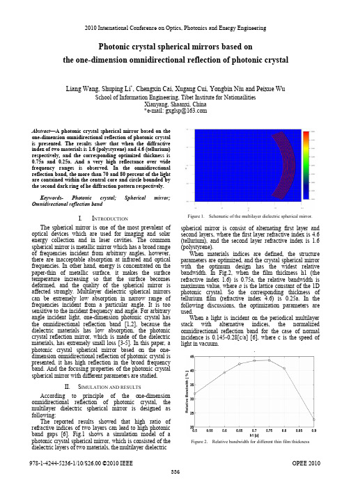
Photonic crystal spherical mirrors based onthe one-dimension omnidirectional reflection of photonic crystal Liang Wang, Shuping Li*, Chengxin Cai, Xugang Cui, Yongbin Niu and Peixue Wu School of Information Engineering, Tibet Institute for NationailitiesXianyang, Shaanxi, China*e-mail: gxglsp@Abstract—A photonic crystal spherical mirror based on the one-dimension omnidirectional reflection of photonic crystalis presented. The results show that when the diffractive index of two materials is 1.6 (polystyrene) and 4.6 (tellurium) respectively, and the corresponding optimized thickness is 0.75a and 0.25a. And a very high reflectance over wide frequency ranges is observed. In the omnidirectional reflection band, the more than 70 and 80 percent of the light are contained within the central core and circle bounded by the second dark ring of he diffraction pattern respectively.Keywords- Photonic crystal; Spherical mirror; Omnidirectional reflection bandI. I NTRODUCTIONThe spherical mirror is one of the most prevalent of optical devices which are used for imaging and solar energy collection and in laser cavities. The common spherical mirror is metallic mirror which has a broad rangeof frequencies incident from arbitrary angles, however, there are inacceptable absorption at infrared and optical frequencies. In other hand, energy is concentrated on the paper-thin of metallic surface, it makes the surface temperature increasing so that the surface becomes deformed, and the quality of the spherical mirror is affected strongly. Multilayer dielectric spherical mirrors can be extremely low absorption in narrow range of frequencies incident from a particular angle. It is too sensitive to the incident frequency and angle. For arbitrary angle incident light, one-dimension photonic crystal has the omnidirectional reflection band [1,2], because the dielectric materials has low absorption, the photonic crystal reflection mirror, which is made of the dielectric materials, has extremely small loss [3-5]. In this paper, a photonic crystal spherical mirror based on the one-dimension omnidirectional reflection of photonic crystal is presented, it has high reflection in the broad frequency band. And the focusing properties of the photonic crystal spherical mirror with different parameters are studied.II. S IMULATION AND RESULTSAccording to principle of the one-dimension omnidirectional reflection of photonic crystal, the multilayer dielectric spherical mirror is designed as following:The reported results showed that high ratio of refractive indices of two layers can lead to high photonic band gaps [6]. Fig.1 shows a simulation model of a photonic crystal spherical mirror, which is consisted of thedielectric layers of two materials, the multilayer dielectricFigure 1. Schematic of the multilayer dielectric spherical mirror. spherical mirror is consist of alternating first layer and second layers, where the first layer refractive index is 4.6 (tellurium), and the second layer refractive index is 1.6 (polystyrene).When materials indices are defined, the structure parameters are optimized, and the crystal spherical mirror with the optimum design has the widest relative bandwidth. In Fig.2, when the film thickness h1 (the refractive index 1.6) is 0.75a, the relative bandwidth is maximum value, where a is the lattice constant of the 1D photonic crystal. So the corresponding thickness of tellurium film (refractive index 4.6) is 0.25a. In the following discussions, the optimization parameters are used.When a light is incident on the periodical multilayer stack with alternative indices, the normalized omnidirectional reflection band for the case of normal incidence is 0.145-0.28[c/a] [6], where c is the speed of light in vacuum..Figure 2. Relative bandwidth for different thin film thickness2010 International Conference on Optics, Photonics and Energy Engineering978-1-4244-5236-1/10/$26.00 ©2010 IEEE OPEE 2010Figure 3. The reflection spectrum for the photonic crystal sphericalmirror with different curvature radii.However, for the photonic crystal spherical mirror with the optimization parameters, the normalized frequency band of the omnidirectional reflection is 0.16-0.285[c/a] which is shown in Fig.3. In the following, the transmission performance of spherical mirror in this frequency band is studied by numerical simulations using finite-difference time-domain method.It is well known that when a light beam is focused by lens, the position of axial intensity maximum of the diffracted wave deviates from the geometrical focus, but it is closed to the lens. It is also fit to the spherical mirror. A light is incident on the photonic crystal spherical mirror, the waist of the beam emerging from the spherical mirror dose not at the geometric focus, the location of the waist is called diffraction focus, the plane local at this point is called diffraction focal plane. The fraction of the total energy contained within central core of the diffraction pattern in the geometric focal plane and diffraction focal plane for the photonic crystal spherical mirror with different curvature radii are shown in Fig.4 and Fig.5 respectively.Figure 4. The fraction of the total energy contained within central core of the diffraction pattern in the geometric focal plane for the photoniccrystal spherical mirror with different curvature radii.Figure 5. The fraction of the total energy contained within central core of the diffraction pattern in the diffraction focal plane for the photoniccrystal spherical mirror with different curvature radii.For the different curvature radii, it is very clearly that the more than 70 percent of the light are contained within the central core in the diffraction focal plane, and the less than 70 percent of the light are contained within the central core in the geometric focal plane except for curvature radius of 5 micron. And the curves in the diffraction focal plane are almost flat in the omnidirectional reflection band. However, in this band, the curves looks like step curves in geometric focal plane when the curvature radius is larger than 25, and with the radius of curvature increasing, the step point move to the high frequency.Fig.6 and Fig.7 show that the more than 80 percent of the light are contained within circle bounded by the second dark ring of he diffraction pattern in the diffraction focal plane, and energy ratio is less than 80 percent of the light in the geometric focal plane except for curvature radius of 5 micron. And in the omnidirectional reflection band, the curves in the diffraction focal plane are almost flat, but the curves looks like step curves in geometric focal plane when the curvature radius is larger than 25, and the step point moves to the high normalization frequency with thecurvature radius increasing.Figure 6. The fraction of the total energy contained within circle bounded by the second dark ring of he diffraction pattern in the geometric focal plane for the photonic crystal spherical mirror withdifferent curvature radii.Figure 7. The fraction of the total energy contained within circlebounded by the second dark ring of he diffraction pattern in thediffraction focal plane for the photonic crystal spherical mirror withdifferent curvature radiiIII. C ONCLUSIONA photonic crystal spherical mirror is consist of alternating first layer and second layers, where the first layer refractive index is 4.6 (tellurium), and the second layer refractive index is 1.6 (polystyrene), the corresponding optimized film thickness is 0.25a and 0.75a respectively. And for these parameters, a broad normalization frequency band is observed, and the transmission performance is studied. Compared with the focusing performance curves for photonic crystal spherical mirrors with different parameters, in the omnidirectional reflection band, in the diffraction focal plane, the more than 70 and 80 percent of the light are contained within the central core and circle bounded by the second dark ring of he diffraction pattern respectively. It has high focusing capacity and a wide range of frequencies and at the same time is of low loss.R EFERENCES[1] J. N. Winn, Y.Fin, S.Fan and J. D. Joannopoulos, “Omnidirectionalreflection from a one-dimensional photonic crystal,” Opt. Letters, vol. 23, pp. 1573-1575, October 1998[2] Y. Fink, J. N. Winn, S. Fan, C. Chen, J. Michel, J. D. Joannopoulosand E. L. Thomas, “A Dielectric Ominidirectional Reflector,”Science, vol. 282, pp. 1679-1682, November 1998.[3] E. Yablonovitch., “Inhibited spontaneous emission in solid-statephysics and electronics,” Phys. Rev. Lett., vol. 58, pp. 2059-2062, May 1987.[4] S. John, “Strong localization of photons in certain disordereddieletric superlatices,” Phys. Rev. Lett., ,vol. 58, pp. 2486-2489, June 1987[5] W. H. Southwell, “Omnidirectional mirror design with quarter-wave dieletric stacks,” Appl. Opt. , vol. 38, pp. 5464-5467, September 1999.[6] B. Temelkuran, E. L. Thomas, J. D. J oannopoulos,and Y. Fink., “Low-loss infrared dielectric material system for broadband dual-range onmidirectional reflectivity,” Opt. Lett., vol. 26, pp. 1370-1372, September 2001。
石墨烯氢气影响on

Effects of Hydrogen Partial Pressure in the Annealing Process on Graphene Growth
Da Hee Jung,† Cheong Kang,† Minjung Kim,‡ Hyeonsik Cheong,‡ Hangil Lee,*,† and Jin Seok Lee*,†
© 2014 American Chemical Society
■
metal catalyst,13,18 the carbon source,19 carbon segregation from metal−carbon melts,20 and the reaction parameters used during CVD growth.21−23 Recently, it was reported that graphene growth is strongly dependent on the hydrogen (H2) contribution during growth time, where it seems to act both as an activator for the formation of surface-bound carbon and as an etching reagent affecting the morphology of the graphene domains.24 Thus, the growth rate and shape of graphene domains rely on the partial pressure of H2 mixed with Ar as the buffer gas.24 Although the role of H2 during growth time was identified, its role during annealing was not stated in detail and remained unclear. In this research, we focused on understanding the role of H2 during the annealing process as well as the growth process in order to control the growth rate and shape of graphene domains. We chose atmospheric-pressure CVD, as it was technologically more accessible for the desired production of graphene. To elucidate the role of H2 in the mixture gas, we synthesized graphene domains on a Cu foil with various volume ratios of H2 to Ar gas and carefully investigated the size, morphology, and composition of the as-produced graphene domains using scanning electron microscopy (SEM), microRaman spectroscopy, energy-dispersive X-ray spectroscopy (EDX) analysis, and high-resolution photoemission spectroscopy (HRPES).25 Based on our observation and characterization of as-produced graphene domains, we present the key reaction details for each growth process and a proposed growth
介质中光的加权路径积分

介质中光的加权路径积分英文回答:The weighted path integral of light in a medium is a measure of the optical path length of light as itpropagates through the medium. It is defined as theintegral of the optical path length along the path of light, weighted by the probability of the light taking that path. The optical path length is the distance that light travels multiplied by the refractive index of the medium. The probability of the light taking a particular path is determined by the laws of geometric optics.The weighted path integral of light can be used to calculate a variety of optical properties of media, such as the refractive index, the absorption coefficient, and the scattering coefficient. It can also be used to designoptical devices, such as lenses and waveguides.中文回答:介质中光的加权路径积分是指光在介质中传播时光程的度量。
其定义为光线沿其路径的光程积分,按光线沿该路径传播的概率加权。
傅里叶光学导论英文
傅里叶光学导论英文IntroductionFourier Optics Introduction is a book that delves into the various theories of wave optics and analyses them in a manner that is easy to comprehend. This article focuses on breaking down the essential points of the book.Step 1: Understanding Fourier OpticsFourier Optics is a branch of optics that involves the study of the fundamental principles governing the propagation of wavefronts through optical devices. It also involves analyzing the response of the devices in the presence of various external stimuli. Fourier optics often uses mathematical techniques such as Fourier transforms, partial differential equations, and matrix algebra to represent the interaction between waves and optical elements.Step 2: Understanding wavefronts and diffractionWavefronts are the surfaces that are defined by the peaks and troughs of an electromagnetic wave. Diffraction refers to the bending of waves as they interact with a surface or an object.Materials and surfaces exhibitdiffraction when light interacts with them. Fourier optics examines the way that light bends and interacts with matter.Step 3: Understanding optical devicesOptical devices include a wide range of instruments such as lenses, mirrors, gratings and filters. Fourier optics studies the way that light interacts with these instruments and how they can be used to alter the properties of light.Step 4: Understanding Fourier TransformsFourier transforms are mathematical techniques that allow the transformation of a time function in the frequency domain. In Fourier optics, this technique is applied to the analysis of a wavefront, which is broken down into a complex amplitude.Step 5: Applications of Fourier OpticsFourier Optics has numerous applications in a variety of fields. For instance, it is used in microscopy to produce sharper images, in spectroscopy to analyze the properties of light, and in holography to produce 3D images.ConclusionFourier Optics Introduction serves as an important tool for engineers and scientists who work with optics. It provides a straightforward explanation of wave optics and how it relates to the devices used for various applications. It also demonstrates how mathematical techniques can be used to understand the interaction of light with matter. Overall, it is an essential resource for anyone who wishes to gain a deeper understanding of optics.。
光电子技术部分翻译

当p型结很窄时,一些注入p结的电子通过扩散和浅层电子复合到达表面, 这种非辐射结合过程降低了光能输出.另外,如果这种复合发生在一个相对大的容器中,由于长的电子扩散长度, 扩散光子的再吸收的可能性变大,再吸收根据材料的容积增加而增加
第四章;stimulated emission devics lasers 受激辐射发射器件
which results in the annihilation of an electron from the CB and a hole in the VB.the excess energy of the electron falling from CB to VB in certain semiconductors,such as GaAs and InP,is emitted as a photon.In Si and Ge,the excess energy is lost as lattice vibrations(heat).In the steaty state,the thermal generation rate is balanced by recombination rate so that the electron concentration n in the CB and hole concentration p in the VB remain constant;both n and p depend on the temperature.
光学专业词汇(1)
absolute optical frequency measurement 绝对光频测量; 绝对光频测量absorpting loss in optical thin-film 光学薄膜的吸收损耗console optical-display plotter 控制台光显示绘图仪continuous variable optical attenuator 连续可变光衰减器continuous-wave optical ranging system 连续波光学测距系统convex optical tool 光学玻璃凸面磨具coronal optical polarization 日冕光学偏振coupled optical resonators 耦合光谐振腔cross-coupling optical beam 交叉耦合光束crown optical glass 冕牌光学玻璃curved holographic optical element 曲面全息光学元件CW optical maser action 连续激光振荡dielectric optical waveguide 介质光波导diffused optical waveguide 扩散光波导digital optical tracking set 数字光学跟踪装置disappearing-filament optical pyrometer 隐丝光学高温计discrete bit optical memory 打点式光存储器; 逐位式光存储器dislocation of optical range-finder 光学测距机的失调dispersive optical system 色散光学系统double resonant optical parameter oscillator 双共振参量振荡器doubly clad optical fibre 双包层光学纤维duct optical cable 管道光缆elasto-optical coefficient 弹光系数electrical isolation optical memory 电隔离光存储器electrical optical converter 电光变换器electrical to optical converter 电光转换器electro-optical beamsplitter 电光分光镜electro-optical converter 电光变换器electro-optical crystal 电光晶体electro-optical detector 电光检测器electro-optical diffraction modulator 电光衍射调制器electro-optical digital deflector 电光数字式偏转器electro-optical guided bomb 电子光学制导炸弹electro-optical hot gas pyrometer 电光热气高温计electro-optical image tube 光电移像管electro-optical light intensity modulator 电光光强度调制器electro-optical light-detecting apparatus 电光测光器; 电光光探测器electro-optical modulator 电光调制器electro-optical multiframe camera 光电多幅照相机electro-optical property 电光性质electro-optical sensor 电光传感器electro-optical shutter 电光快门electro-optical switch 电光开关electro-optical system 光电系统electro-optical tracker system 光电跟踪系统electro-optical tube 光电管electro-optically tuned laser 电光可调激光器electron optical prism 电子光学棱镜electron-optical aberration 电子光学象差electron-optical image intensifier 电光像增强器electron-optical system 电子光学系统electronic optical comparator 光电比较仪electronically tunable optical filter 电子可调谐光学滤波器equivalent optical thickness of thin film 薄膜等效厚度erasable optical disk 可擦光盘erbium-doped optical fiber amplifier 掺铒光纤放大器etalon optical power 标准光强度external optical density 外光密度fast refractive infrared optical system 快速折射红外光学系统fibre optical device 纤维光学装置fibre optical screen 纤维光学屏幕fibre optically coupled cascaded image intensifier 光纤耦合级联式图像增强器fibre-optical cable 纤维光缆field optical collimator system 场致光学准直仪系统filling material for optical fiber cable 光缆缆芯填充料film optical modulator 薄膜光调制器film optical multiplexer 薄膜光复用器film optical sensing device 胶片光学传感器film optical switch 薄膜光开关film optical waveguide 薄膜光波导flat optical cable 扁平光缆flat optical tool 光学玻璃平面研磨盘flint optical glass 火石光学玻璃fluorozirconate type optical fiber 氟化锆基光纤focusing optical fiber 聚焦光纤; 聚焦光纤Fourier optical imaging system 傅里叶光学成像系统frequency discriminating optical chopper 鉴频光学限制器gallium-arsenide optical filter 砷化镓滤光片gas-discharge optical maser 气体放电光学微波激射; 气体光学脉泽geometric-optical aberration 几何光学像差geometrical-optical approximation 几何光学近似germanium-doped optical fiber 掺锗光学纤维giant optical pulsation 巨光脉动; 巨光脉动giant optical pulse 巨光脉冲; 巨光脉冲glass optical fiber 玻璃光纤graded index optical waveguide 渐变折射率光波导graded-index optical fiber 渐变折射率光学纤维graphical design of optical system 光学系统图解设计ground-based optical receiver 地面光学接收机; 地面光学接收器gyro erected optical navigation 陀螺光学导航heat treatment of optical crystal 光学晶体热处理heteroepitaxial optical waveguide 异质外延光波导high birefringence optical fiber 高双折射光纤high performance optical cable connector 高性能光缆连接器high precision optical plate 高精度光学平板high repetition rate optical pulse 高重复率光脉冲high speed optical switch 高速光学开关high speed-optical switch 高速开关high strength optical fiber 高强度光纤high temperature optical fiber sensor 高温光纤传感器high-resolution optical mask 高分辨率光学掩膜high-resolution optical memory 高分辨率光存储器holographic optical elements (HOE) 全息光学元件homogeneous optical waveguide 均匀光学波导; 均匀光学波导hybrid optical cable connector 混合式光缆连接器hybrid optical fiber sensor 混合式光纤传感器image dividing optical system 光学分像系统image optical reconstruction 图像光学恢复image spliting optical system 影像分光系统image-dividing relay optical system 分像转向光学系统incoherent optical arrangement 非相干光学装置incoherent optical converter 非相干光转换器incoherent optical information processing 非相干光信息处理incoherent optical radar 非相干光学雷达inelastic optical scattering 非弹性光散射infrared optical fiber 红外光纤infrared optical material 红外光学材料infrared optical measuring system 红外光学测量系统inserting optical cable connector 插入光缆连接器inspection of optical crystal 光学晶体检验integrated optical bolometer for radiation 集成光学辐射热测量计integrated optical circuit 集成光路; 集成光学电路integrated optical spectrum analyzer 集成光谱分析器integrated optical switch 集成光学开关integrated optical waveguide coupler 集成光学波导耦合器intercept ground-based optical recorder 监视地面光学记录仪interferometric optical fiber acoustic sensor 干涉型声光纤声传感器internal optical density 内光密度; 内光学密度internal optical parametric oscillation 内光学参量振荡internal optical parametric oscillator 内光学参量振荡器Kerr electro optical law 克尔电光定律lamp bulb for optical pyrometer 光学高温计用灯泡large aperture optical system 大孔径光学系统large optical cavity laser 大光腔激光器large optical reflector 大型反光镜large optical-cavity diode 大光腔二极管large optical-cavity laser diode 大光腔激光二极管laser damage of optical coatings 光学镀层激光损伤laser optical bench 激光器光具座laser optical demonstration instrument 激光光学演示仪leaf optical system 薄片光学系统lens optical length 镜头光学长度; 镜头光学长度light splitting optical system 分束光学系统light-splitting optical system 分光光学系统LiNbO�3 optical parametric oscillator 掺镁铌酸锂光参量振荡器linear electro-optical effect 线性电光效应liquid-core optical fibre 液芯光纤loaded diffused optical waveguide 加载扩散光波导long haul optical link 长距离光线路longitudinal fundamental optical frequency 纵向光学基频率lunar optical altimeter 登月用光学测高计magnet-optical memory system 磁光存储系统magnetic optical disk 磁光盘magnetic optical-character reader 磁光字符阅读器magnetid-optical devices 磁光器件magneto optical disk 磁光盘magneto optical disk editor 磁光盘编辑器magneto optical driver 磁光盘驱动器magneto optical semiconductor laser 磁光半导体激光器magneto-optical modulator 磁光调制器magneto-optical phenomenon 磁光现象magneto-optical shutter 磁光开关mass optical memory 大容量光存储器mechanical optical comparator 机械光学比较仪mechanical optical switch 机械光开关mechanically-driven optical reflector 机械传动光反射器medical optical instrument 医疗光学仪器; 医用光学仪器metal-clad optical waveguide 金属包层光学波导meteorological optical range 气象光学视距; 气象能见度military optical instrument 军用光学仪器; 军用光学仪器mirror-optical system 反射镜光学系统mobile optical tracking unit (MOTU) 机动光学跟踪装置mode of optical cavity 光学共振腔模; 共振腔的振荡模modular opticaltest instrument for fiber 模块化光纤光学测试仪monomode optical fiber 单模光纤monomode optical waveguide 单模光波导monopulse optical receiver 单脉冲光接收器multi-fiber optical cable 多芯电缆multi-fiber optical submarine cable 多芯海底光缆multichannel optical analyzer 多通道光学分析器multichannel optical cable stranding machine 多路光缆绞制机multicomponent glass optical fiber 多组分玻璃光纤multifont optical arena 多字体识别器multimode optical cable 多模光缆multimode optical fiber 多模光导纤维; 多模光纤multimode optical fiber hydrophone 多模光纤水听器multireflector optical resonator 多反射镜光学共振器naval gun optical director 舰炮光学指挥仪non-coherent Fourier-optical imaging system 非相干傅里叶光学成像系统non-coherent optical carrier 非相干光学载波non-coherent optical computer 不相干光学计算机non-coherent optical detector 非相干光检测器; 非相干光探测器non-coherent optical processing system 非相干光处理系统non-erasable optical disk 不可擦光盘non-metallic type optical cable 非金属型光缆non-optical propagation 封闭通道传播non-polar optical scattering 非偏振光散射nondestructive readout optical memory 无损读出光存储器nonlinear optical coefficient 非线性光学系数nonlinear optical crystal 非线性光学晶体nonlinear optical effect 非线性光学效应nonlinear optical phenomena 非线性光学现象nonlinear optical processing 非线性光学处理nonlinear optical response 非线性光学响应nonlinear optical susceptibility 非线性光极化率numerical designation of optical glass 光学玻璃标号offset optical square 偏距光学直角头omnidirectional optical scanner 全向光学扫描器on-board optical system 机载光学系统optical 光学的; 旋光; 视力的optical aberration 光学像差; 像差; 象差optical absorption 光的吸收; 光学吸收optical absorption band 光吸收带optical absorption edge 光吸收限; 光学吸收限optical access coupler 光学取数耦合器optical accessory 光学附件optical achromatism 可见光消色差性optical acquisition 光学捕获optical acquisition equipment 激光捕获装置optical active phonon 光激活声子optical active substance 光活性物质optical activity 光学活性; 旋光度; 旋光性optical activity of oil 石油的旋光性optical adaptive technique 光自适应技术; 光学自适应技术optical admittance 光学导纳optical agnosia 视觉性认识不能optical aid 光学辅助工具optical air mass 光学空气质量; 大气光学质量optical alignment 光学调准; 光学装校; 光学准直optical alignment equipment 光学校准设备optical alignment unit 光学校准设备optical altimeter 光学测高计; 光学高度计optical ammeter 光学安培计; 光学电流计optical amplification 光放大optical amplifier 光放大器; 光学放大器optical amplifier bandwidth 光放大器带宽optical amplitude modulator 光调幅器; 光振幅调制器optical analog 光学模拟optical analog device 光学模拟装置optical analog memory 光模拟存储器optical analog transform technique 光学模拟变换技术optical analogue computer 光学模拟计算机optical analyser 光学检偏振器optical analysis 光学分析optical analyzer 光学分析器; 光学检偏镜optical anemometer 光学风速计optical angle gauge 光学测角仪optical angular motion sensor 光学角运动传感器optical anisotropy 光学的各向异性; 光学各向同性; 光学异向性optical anomaly 光反常; 光性异常; 光学反常; 光学性反常optical antenna 光波段天线; 光学天线optical antenna angle 光学天线张角optical antenna aperture 光学天线孔径optical antenna gain 光学天线增益optical antipode 光对映体; 旋光对映体antipode,optical isomer, antimers 对映体optical appearance 光学外观optical approach 用光学仪器接近optical arm 光学臂optical arrangement 光学装置optical arteriovenous oximeter 光学动静脉血氧定量计optical artware 光学工艺品optical aspherical surface 光学非球面optical astrometry 光学天体测量学optical astronomy 光学天文学optical astrophysics 光学天体物理学optical asymmetry 光学不对称optical attenuator 光衰减器; 光学衰减器optical automatic titrimeter 光学自动滴定仪optical avalanche laser 光学雪崩式激光器optical axial figure 光轴图形optical axial plane 光轴平面optical axis 光轴; 视轴optical axis of crystal 晶体光轴optical axis of symmetry 光学对称轴optical baffle 光学隔板optical balance 光学补偿; 光学天平optical band 光波段optical band gap 光禁带optical bandpass filter 光带通滤光器; 光学带通滤光片optical barmonic generation 光学谐波振荡optical beacon 光指向标optical beam deflection 光束偏转optical beam expander 光束扩张器optical beam flying 光束扫描optical beam riding 光波束引导optical beam scanner 光束扫描器optical beam splitter 光束分光镜optical beam-direction control 光束方向控制optical bench 光具座optical bevel protractor 光学量角器; 光学斜度规optical binary 光学双星optical biosensor 光生物传感器optical bistability 光学双稳态optical black 光学黑体optical blacking 光学黑色涂料optical bleaches 荧光增白剂optical boroscope 光学缺陷探测仪optical branch 光频支optical branching device 光分路器optical branching filter 光分路滤波器optical bridge circuit 光桥路optical brightener 光学增亮剂optical brightness 光学亮度optical Brinell hardness tester 光学布氏硬度计optical cable 光导电缆optical cable assembly 光缆组件optical cable connector 光缆连接器optical cable driver 光缆激励器optical calculating machine 光计算机optical calculation 光学计算optical calibration 光学仪器检定optical caliper 光学校准器optical calliper 光学轮尺optical card reader 光学读卡器optical cardan link 光控万向关节optical carrier 光学载波optical cavity 光共振腔optical cavity diode 光腔二极管optical cavity laser interferometer 光谐振激光干涉仪optical cavity mirror sensor 光腔镜式传感器optical cavity mode 光学共振腔模optical cavity modes 光学共振腔模式optical cement 光胶; 光学胶; 光学胶合剂optical center 光心; 光学中心optical center of lens 镜片光心; 镜片光心optical centering and edging 光学定心磨边optical centering device 光学对中器optical ceramics 光学陶瓷optical channel 光波道; 光通道optical channel-dropping filter 光通道衰减滤光器optical character 光学特性optical character reader 光符号阅读器optical character reader (OCR) 光标阅读机; 光符阅读机; 光学字符读出器; 光字符阅读机optical character recognition 光学阅读机optical character recognition (OCR) 光标识别; 光符号识别; 光符识别; 光学符号读出; 光学字符识别optical character recognition common language 光学符号识别通用语言optical character recognition machine 光符号识别机; 光学符号识别机; 光学字符辨识机optical character recognition reader 光学字符阅读器optical character recognition system 光符号识别系统; 光字符识别系统optical character recognition teleprinter 光学字符识别电传打字机optical character scanner 光学字符扫描器optical characteristics 光学特性optical check 光学检验optical choledochoscope 光学胆道镜optical chopper 光断续器; 光斩波器optical cine duplicating machine 光学印片机optical circle 光学度盘optical circular table 光学圆分度台optical circulator 光环行器; 光学循环器optical clinometer 光学测斜仪; 光学倾斜仪optical clouration 光学着色optical coating 光学镀层; 光学镀膜; 光学涂层optical code reader 光学代码阅读器optical code reading wand 光码读数杆optical coincidence index 光重合比孔索引optical collector 聚光器; 聚光器; 集光器optical colorimetry 目视比色法optical colourimeter 光学色度计optical combiner 光组合器optical communication 光学通信optical communication channel 光通信信道optical communication link 光学通信线路optical communication receiver 光通信接收机optical communication system 光通信系统optical communication technique 光通信技术optical commutation circuit 光开关电路optical comparator 光学比较仪optical compensating system 光学补偿系统optical compensation 光学补偿optical compensation camera 光学补偿摄影机optical compensator 光学补偿器optical component 光学部件; 光学子星optical computer 光计算机; 光学计算机optical computing 光学计算optical conduction 光传导optical conductivity 光电导率optical conductor 光导体optical conductor loss 光导体损耗optical connector 光连接器optical constant 光学恒量optical constants 光学常数optical contact 光接触; 光学接触optical continuum 光连续区optical contour grinder 光学轮廓磨床; 光学曲线磨床optical contrast 光学衬比optical contrast ratio 光对比度optical contraster 光学增衬器optical converter 光学变换器optical convolution 光学卷积optical coordinate measuring apparatus 光学坐标测量仪optical corner reflector 光学直角反射器optical correction 光学校正; 光学修正; 视觉改正optical correlation 光学相关optical correlator 光相关器optical counter-rotating wedges 反向旋转光楔optical countermeasures 光学对抗optical counterpart 光学对应体optical coupler 光隔离器; 光耦合器optical coupling 光耦合optical cross section 光学截面optical cross-section 光截面optical crosstalk 光学串扰; 串光optical crown 光学冕玻璃optical crystal 光学晶体optical crystallography 晶体光学optical current metre 光学流速仪optical curve grinding machine 光学曲线磨床optical cycle 光学周期optical damage 光学损伤optical damage threshold 光学损伤阈optical data 光学数据optical data bus (母线) 光数据总线optical data corrector 光学数据校正器optical data digitizer 光学数据数字化器optical data handling 光学数据处理optical data processing 光学数据处理optical data processing system 光学数据处理系统optical data processor 光学数据处理机optical data transmission channel 光数据传输通道optical datatransmission channel 光数据传输信道; 光学数据传输信道optical decoy 光假目标; 光学假目标optical defect 光缺陷; 光学缺陷optical defects of crystals 晶体光学缺陷optical deflection 光偏转; 光学偏移optical deflectometer 光学弯度计optical deflector 光偏转器optical deformation 光学形变optical delay circuit 光学延迟回路; 光延迟电路optical delay line 光延迟线optical demultiplexer 光解多路复用器optical densitometer 光密度计optical densitometric method 光密度法optical densitometry 光密度测量术optical density 光密度optical density (OD) 光学密度optical density colour 光密度色度optical depression 旋光性降低optical depth 光深; 光学深度optical design 光学设计optical design optimization 光学设计最佳化optical design procedure 光学设计程序optical designation 光学标号optical detection 光学探测optical detector 光辐射探测器; 光检测器; 光学探测器optical detector of the trajector 光学弹道测量装置optical detector technology 光探测技术optical device 光学装置optical diameter 光学直径optical dichroism 光学二向色性optical dielectric constant 光介电常数; 光频介电常数optical diffraction image 光衍射图像optical diffractometer 光衍射计optical digital audio player 光学数字音频唱机optical digital computer 光数字计算机; 光学数字计算机optical digital tachometer 光学数字转速表optical dilatometer 光学膨胀计optical dimming 光学模糊optical diode 光二极管optical direct vision finder 光学直视寻像器optical direction and ranging 光学定向和测距optical direction finder 光学定向器optical direction finding 光学测向optical directional coupler 光定向耦合器; 光学定向耦合器optical directional filter 定向滤光器optical disc 光盘; 光学刻度盘optical disk 光盘; 光学视面optical disk cartridge 光盘盒optical disk control card 光盘控制卡optical disk recorder 光盘录像机optical disk system 光盘系统optical dispersion attenuation 光色散衰减optical displacement sensor 光学式位移传感器; 光学位移传感器optical display keyboard 光显示键盘optical display plotter 光显示绘图仪optical display terminal 光显示终端; 光显示终端设备optical distance 光程; 光学距离; 可见距离optical distance meter 光学测距仪optical distortion 光畸变; 光学畸变; 光学扭曲optical disturbance 光扰动optical dividing head 光学分度头optical dividing head with projection readout 光学投影读数分度头optical dividing table 光学分度台optical document reader 光文件阅读机optical Doppler effect 光学多普勒效应optical Doppler radar 多普勒光雷达optical dosimeter 光学辐射剂量计optical double 视双星optical double star 光学双星optical doublet 光学双线optical doublet star 光学双星optical driver 光盘驱动器optical dust instrument 光学测尘仪optical dynameter 光学倍率计optical echo 光学回波optical efficiency 光效率optical electric axial angle encoder 光电轴角编码器optical electron 光学电子optical electronic reproducer 光声头optical electronic transducer 光电换能器optical electronics 光电子学optical element 光学零件; 光学元件optical emission line 光学发射线optical emission spectrograph 发光摄谱仪optical emission spectrography 发光摄谱学; 发射光谱学optical enantiomorph 旋光对映体optical encoder 光编码器; 光学编码器; 光学同步发射机optical endfinish 光学端面光洁度optical endoscope 光内窥镜optical energy 光能optical energy density 光能密度optical engineering 光学工程optical enlargement 光学放大optical EPR Gauss meter 光学电子顺磁共振高斯计optical equipment 光学设备optical equivalence 光学等效optical evaluation facility 光学检验设备optical exaltation 旋光性增强optical excitation 光激发optical excited atom 光激发原子optical excited laser 光激发激光器; 光激励型激光器optical exciting pulse 光激发脉冲optical exitation rate 光激励率optical exposure meter 光学曝光表optical extensometer 光学伸长仪optical eye level finder 光学直视水平瞄准器optical fabrication 光学加工optical Farday rotation isolator 光学法拉第旋转隔离器optical fault locator 光故障定位器optical feedback 光反馈optical feedback image intensifying system 光学反馈图像增强系统optical feeler 光学接触器optical fiber 光导纤维; 光学纤维optical fiber cable 光导纤维电缆; 光缆optical fiber cable for hybrid communication 混合通信光缆optical fiber cable for installation in duct 管道敷设式光缆optical fiber cavity 纤维光腔optical fiber composite connector 复合式光纤连接器optical fiber cystoscope 光导纤维膀胱镜optical fiber interferometer 光导纤维干涉仪optical fiber plate 光导纤维板optical fiber resonator 光学纤维谐振腔optical fiber ribbon cable 带状光缆optical fiber tube 光导纤维管optical fibre 光纤optical fibre abruption tester 光纤断裂测试器optical fibre acoustic sensor 光纤声压传感器optical fibre active connector 光纤有源连接器optical fibre amperemeter 光纤电流计optical fibre amplifier 光纤放大器optical fibre amplifier multiplexer 光纤放大器多路复用器optical fibre biosensor 光纤声压传感器optical fibre bundle 光纤束optical fibre cable stranding machine 光纤成缆机optical fibre chemical sensor 光纤化学传感器optical fibre communication 光纤通信optical fibre communication repeater 光纤通信中继器optical fibre compression sensor 光纤压力传感器optical fibre concentrator 光纤集中器optical fibre connector 光纤连接器optical fibre coupler 光纤耦合器optical fibre current sensor 光纤电流传感器optical fibre demultiplexer 光纤解多路复用器optical fibre dispenser 光纤松放器optical fibre dispersion tester 光纤色散测试仪optical fibre displacement sensor 光纤位移传感器optical fibre electric field strength sensor 光纤电场强度传感器optical fibre flowmeter 光纤流量计optical fibre fusion splicer 光纤熔接器optical fibre gyro 光纤陀螺optical fibre gyroscope 光纤陀螺仪optical fibre helical microbend sensor 光纤螺旋微弯传感器optical fibre hydrophone 光纤水听器optical fibre image sensor 光纤图像传感器optical fibre interferometric sensor 光纤干涉传感器optical fibre ion sensor 光纤离子传感器optical fibre line-tocircle converter 光纤圆直变换器optical fibre magnetic field strength sensor 光纤磁场强度传感器optical fibre magnetostrictive sensor 光纤磁致伸缩传感器optical fibre monitor 光纤监控器optical fibre multiplexer 光纤多路复用器optical fibre pickoff coupler 光纤传感耦合器; 光纤发送耦合器optical fibre polarizer 光纤偏振器optical fibre proof-tester 光纤检验机optical fibre pulse compression 光纤脉冲压缩optical fibre radiation sensor 光纤射线传感器optical fibre resonator 光纤共振腔; 光纤谐振器optical fibre rewinder 光纤复绕机optical fibre ringer 光纤振铃器optical fibre rotator 光纤旋转器optical fibre sensor 光纤传感器optical fibre sound pressure sensor 光纤声压传感器optical fibre strander 光纤绞线器optical fibre temperature sensor 光纤温度传感器optical fibre thermometer on thermal colour effect 光纤热色效应温度计optical fibre transmission 光纤传输optical fibre transmission facilities 光纤传输设备optical fibre ultrasonic sensor 光纤超声传感器optical fibre velocity sensor 光纤速度传感器optical fibre vibration sensor 光纤振动传感器optical fibre voltage sensor 光纤电压传感器optical fibre wavelength division multiplexer 光纤波分复用器optical field 光场optical field effect transistor 光场效应晶体管optical figuring 光学修整optical film-fibre coupler 光薄膜纤维耦合器optical filming 光学镀膜optical filter 滤光片; 滤光器; 滤色镜optical filter box 滤光片组件optical filter gas analyzer 光学滤波式气体分析器optical filter predetection 检波前光学滤光片optical finder 光学取景器; 光学寻像器optical finishing 光学精加工optical fire director 光学射击指挥仪optical firecontrol instrument 光学射击控制仪器optical fixed reticule sight 光学固定环瞄准具optical flame detector 光感器optical flat 光学平板; 光学平度; 光学平面; 光学平行平板玻璃; 平晶optical flat gauge 光学平面规optical flat glass 光学平玻璃optical flat glass filter 光学玻璃滤色镜optical flatness 光学光滑度; 光学平度; 光学平滑度; 光学平直度optical flatness gauge 光学平直仪optical flint glass 火石光学玻璃optical fluid-flow measurement 光学流体流动测量法optical flux 光通量optical foam 光学泡沫optical focus 光焦点optical focus switch 光聚焦开关; 光学聚焦转换开关optical focusing 光聚焦optical focusing device 光学聚焦装置optical fog 光学灰雾optical font 光符识别用字体; 光识别字体; 光学识别字体; 光学字体optical force 矫形力optical foresight 光学瞄准器optical Fourier analysis method 光学傅里叶分析法optical Fourier transform 光学傅里叶变换optical free induction decay 光学无感生衰减optical frequencies 光频段optical frequency 光频optical frequency amplifier 光频放大器optical frequency branch 光频支路optical frequency converter 光频变换器optical frequency division multiplex 光频分复用optical frequency domain reflectometer 光频域反射计optical frequency mixing 光混频optical frequency shift 光频移optical frequency translation 光频变换optical fundus 眼底optical fuse 光引信optical gain 光学增益optical galaxy 光学星系optical gate 光闸optical gauge 光学测量仪器optical generation 光波振荡optical generator 光发生器; 光振荡器optical glass 光学玻璃optical glass blank 光学玻璃毛坯optical glass material 光学玻璃材料optical goniometer 光学测角计; 光学测向器optical grating 光栅optical grating measuring system 光栅测量系统optical grid lines 光学光栅刻线optical grinding 光学研磨optical guidance 光学导航; 光学制导; 光制导optical guidance system 光学制导系统optical guiding system 光制导系统optical gyroscope 光陀螺仪optical harmonic 光谐波; 光学谐波optical harness 光缆捆束optical harness assembly 光缆捆束组件optical haze 大型闪烁optical head (投影器) 光度头optical height finder 光学测高仪optical heterodyne 光学外差optical heterodyne detection 光频外差探测optical heterodyne detection system 光外差探测系统optical heterodyne radar 光频外差雷达optical heterodyne receiver 光频外差接收器; 光外差接收机optical heterodyne repeater 光外差中继器optical heterodyne spectroscopy 光频外差光谱学optical heterodyning 光外差作用optical heterogeneity 光学不均匀性; 光学非均匀性optical holographic interferometry 光学全息干涉测量技术optical holography 光学全息术optical homer 光学寻的头; 光学自动跟踪头optical homing 光学自动跟踪optical homing head 光学自动导引头optical homing head axis 光学导引头瞄准轴optical homodyne 光学零差optical homodyne receiver 光零拍接收机; 光学零拍接收机optical homogeneity 光学均匀性optical horizon sensor 光学地平仪optical hygrometer 光学湿度表optical identification 光学证认optical illusion 光幻觉; 视错觉optical image 光学像; 光学影像optical image combinator 光学合像仪optical image converter 光学图像转换器optical image feedback 光学图像反馈optical image formation 光学图像; 光学图像形成optical image processor 光学图像处理器optical image rejection mixer 光图像抑制混频器optical image stabilized telescope 光学稳像望远镜optical image transmission device 光学图像传输装置optical image unit 光学图像输入器optical imagery 光学图像optical imaging device 光学成像装置optical immersed detector 光浸没式探测器optical immersion 光学浸没optical immersion gain 光学浸没增益optical impedance discontinuity 光阻抗突变optical impression 影像optical inactivity 不旋光性optical index 光学指标; 光学指数optical indicator 光学示功计; 光学指示器; 光指示器optical indicatrix 光折射椭球; 光学特性曲线optical inertial guidance and navigation system 光学惯性制导和导航系统optical information 光学信息optical information handling 光学信息处理optical information processing 光学信息处理optical information storage 光信息存储器; 光学信息储存; 光学信息存储optical information transfer 光学信息传递optical inhomogeneity 光学不均匀性optical injection 光学注入optical injector 光注入器optical input 光输入; 可见输入optical instrument 光学仪器optical instrument design 光学仪器设计optical instrument making 光学仪器制造optical instrument mould and fog auto-detector 光学仪器霉雾自动检测仪optical instrumentation 光学仪器设备optical insulation 光学绝缘optical integrated circuit 集成光路optical integration 光学集成optical integrator 光学积分器optical intensity 光强optical interaction 光学相互作用optical interconnection 光学互接optical interface adapter 光接口适配器optical interference 光波干涉; 光学干涉optical interference coating 光学干涉膜optical interference filter 光干涉滤光片; 光学干涉滤光片optical interference measurement 光学干涉测量法optical interference method 光波干涉法optical interference type gas analyzer 光干涉式气体分析器optical interfernece coating 光波干涉膜optical interferometer 光干涉仪; 光学干涉仪optical interferometry 光学干涉量度法optical interval 光学间距; 光学区间optical invariant 光学不变量optical inversion 光学转向optical inversion system 光学转像系统optical ionization energy 光电离能optical iridectomy 光学虹膜切除术optical isolation 光学隔离optical isolator 光隔离器; 光频隔离器; 光学隔离器optical isomer 光学异构体; 旋光异构体optical isomerism 旋光异构; 光学异构optical isotropy 光学各向同性optical jig boring machine 光学坐标镗床optical Kerr effect 光学克尔效应optical laboratory 光学实验室optical lamp 光学灯optical landing system 光学着陆系统optical lantern 幻灯机optical laying 光学瞄准optical laying equipment 光学瞄准器optical length 光程; 光程长optical length scale 光学刻尺optical lens 光学镜片; 光学透镜; 透镜optical lens face 光学透镜面optical lens polisher 光学透镜磨光器optical lens system 光学透镜系统optical lens wave guide 光学透镜波导optical level 光学水平仪optical lever 光杠杆; 光学比长仪; 光学杠杆optical levitation 光学悬浮optical libration 光学天平动optical light filter 光学滤光器optical line of sight 光学瞄准线optical line-scan 光学行扫描optical linescan device 光行扫描器optical link 光线路optical liquid 光学浸液optical lithography 光学制版optical local oscillator 光学本机振荡器optical lock-on 光学跟踪; 光学锁定; 光学自动跟踪optical log 光学测程器; 光学计程仪optical logic operations 光学逻辑功能optical loss test set 光损耗测试仪optical low-pass filter 光学低通滤波器; 低通滤光器optical magnetic probe 光磁探针optical manufacture 光学加工optical mapping 光学映像optical mark card reader 光符号卡读出器optical mark reader 光学标志阅读器optical mark reader (OMR) 光标阅读机; 光字符阅读机optical maser 光激射器; 光量子放大器optical maser oscillator 激光振荡器optical mask 光学掩模optical matched filter 光学匹配滤波器optical matched-filter imagecorrelator 光学匹配滤波像相关器optical material 光学材料optical means 光学方法; 光学装置optical measurement 光学测量optical measurement of distance 光学测距法optical measuring device 光学测量装置optical measuring head 光学测头optical measuring instrument 光学测量仪器optical measuring machine 光学测量机optical measuring system 光学测量系统optical measuring technique 光学测量技术。
- 1、下载文档前请自行甄别文档内容的完整性,平台不提供额外的编辑、内容补充、找答案等附加服务。
- 2、"仅部分预览"的文档,不可在线预览部分如存在完整性等问题,可反馈申请退款(可完整预览的文档不适用该条件!)。
- 3、如文档侵犯您的权益,请联系客服反馈,我们会尽快为您处理(人工客服工作时间:9:00-18:30)。
Optical properties of monolayer transition metal dichalcogenidesprobed by spectroscopic ellipsometryKAUST RepositoryItem type ArticleAuthorsLiu, Hsiang-Lin; Shen, Chih-Chiang; Su, Sheng-Han; Hsu,Chang-Lung; Li, Ming-Yang; Li, Lain-JongCitationOptical properties of monolayer transition metaldichalcogenides probed by spectroscopic ellipsometry 2014, 105 (20):201905 Applied Physics Letters Eprint version Publisher's Version/PDF DOI 10.1063/1.4901836Publisher American Institute of Physics Journal Applied Physics LettersRights Archived with thanks to Applied Physics Letters Downloaded 9-Sep-2015 11:55:07Link to item/10754/346722Optical properties of monolayer transition metal dichalcogenides probed by spectroscopic ellipsometryHsiang-Lin Liu, Chih-Chiang Shen, Sheng-Han Su, Chang-Lung Hsu, Ming-Yang Li, and Lain-Jong LiCitation: Applied Physics Letters 105, 201905 (2014); doi: 10.1063/1.4901836View online: /10.1063/1.4901836View Table of Contents: /content/aip/journal/apl/105/20?ver=pdfcovPublished by the AIP PublishingArticles you may be interested inEnhancement of band-to-band tunneling in mono-layer transition metal dichalcogenides two-dimensional materials by vacancy defectsAppl. Phys. Lett. 104, 023512 (2014); 10.1063/1.4862667Optical properties and phase change transition in Ge 2 Sb 2 Te 5 flash evaporated thin films studied by temperature dependent spectroscopic ellipsometryJ. Appl. Phys. 104, 043523 (2008); 10.1063/1.2970069Optical properties of As 33 S 67 − x Se x bulk glasses studied by spectroscopic ellipsometryJ. Appl. Phys. 103, 083512 (2008); 10.1063/1.2906138Interplay of hydrogen and deposition temperature in optical properties of hot-wire deposited a ‐ Si : H Films: Ex situ spectroscopic ellipsometry studiesJ. Vac. Sci. Technol. A 23, 1668 (2005); 10.1116/1.2056552Optical constants of wurtzite ZnS thin films determined by spectroscopic ellipsometryAppl. Phys. Lett. 79, 3612 (2001); 10.1063/1.1419229Optical properties of monolayer transition metal dichalcogenides probed by spectroscopic ellipsometryHsiang-Lin Liu,1,a)Chih-Chiang Shen,1Sheng-Han Su,2Chang-Lung Hsu,2Ming-Y ang Li,2and Lain-Jong Li 2,b)1Department of Physics,National Taiwan Normal University,Taipei 11677,Taiwan 2Institute of Atomic and Molecular Sciences,Academia Sinica,Taipei 10617,Taiwan(Received 21August 2014;accepted 3November 2014;published online 18November 2014)Spectroscopic ellipsometry was used to characterize the complex refractive index of chemical-vapor-deposited monolayer transition metal dichalcogenides (TMDs).The extraordinary large value of the refractive index in the visible frequency range is obtained.The absorption response shows a strong correlation between the magnitude of the exciton binding energy and band gap energy.Together with the observed giant spin-orbit splitting,these findings advance the fundamental understanding of their novel electronic structures and the development of monolayer TMDs-based optoelectronic andspintronic devices.VC 2014AIP Publishing LLC .[/10.1063/1.4901836]The layered transition metal dichalcogenides (TMDs),including MX 2(M ¼Mo,W;X ¼S,Se,Te),have recently attracted considerable attention due to their novel physical phenomena in reduced dimension and the spatially confined electronic and optical properties.1,2Among them,monolayer TMDs are special in many respects.Most notably,monolayer TMDs have a rather large direct bandgap,making these mate-rials favourable for optoelectronic applications,3–8field-effect transistors,9–11and photovoltaic cells.12Furthermore,both the conduction and valence bands of monolayer TMDs have two energy degenerate valleys at the corners of the first Brillouin zone,which are essential to optically control the charge car-riers in these valleys.13These properties make possible a new class of integration in spintronics and valleytronics.14–16For many of these applications,knowledge of the optical properties of monolayer TMDs is fundamentally important.From photoluminescence characterization,information about the optical bandgap of these materials can be gained.3–8The observed double-peak structure in the optical absorption spectra of monolayer TMDs can be connected to exciton excitations.These excitons are due to the vertical transition at the K point of the Brillouin zone from a spin-orbit-split va-lence band to doubly degenerate conduction band.17Despite the intense research on the optical properties of monolayer TMDs,no studies of their wavelength-dependent complex refractive index have been done to date.Measurements of the refractive index and extinction coefficient spectra of monolayer TMDs over a wide frequency range can provide useful information about optical and electronic properties that devices based on these materials may possess.In this paper,we combine a spectroscopic ellipsometry with a series of monolayer TMDs materials to more deeply explore their optical constants ranging from the near-infrared to the deep-ultraviolet.Spectroscopic ellipsometry allows the determination of a material’s optical functions,such asrefractive index and extinction coefficient,and thickness of thin films in a nondestructive manner.18We find that monolayer MoS 2displays extraordinary large value of the re-fractive index about 6.50at 450nm.It decreases to 4.25at 540nm for monolayer MoSe 2.Moreover,the absorption edge in extinction coefficient spectra reveals that monolayer WS 2has the largest band gap of about 2.11eV.It decreases to 1.62eV for monolayer MoSe 2.Notably,a direct correla-tion is observed between the magnitude of bang gap and exciton binding energy in monolayer TMDs.Additionally,the spin-orbit splitting energy of monolayer TMDs increases as the fourth power of the atomic number of the constituent elements.This work advances the development of monolayer TMDs materials with coexisting optoelectronic and spin-tronics device components.Monolayer TMDs thin films,such as MoS 2,MoSe 2,WS 2,and WSe 2,were deposited onto sapphire substrates by chemical vapor deposition.19–22These thin films were high-quality single layer materials verified using atomic force microscopy.19–22Micro-Raman scattering spectroscopy was also performed to characterize the thickness and structural quality of the thin films.The experimental results of several points across the thin films indicate one layer signature.19–23Ellipsometric spectra were collected under multiple angles of incidence between 60 and 75 using a Woollam M-2000U rotating compensator multichannel spectroscopic ellipsometer over a spectral range from 0.73to 6.42eV.The reproducibility of the spectra were also confirmed at three different spots on the thin films using a specially designed focusing optics coupled with spectroscopic ellipsometry for the spot (100Â100l m 2)measurements.The complex dielectric func-tions of monolayer TMDs thin films were extracted using least-squares regression analysis and weighted root-mean-square error to fit the ellipsometric spectra to a stacked layer model consisting of sapphire substrate/thin film/surface rough-ness/air ambient structure.The parameters of the stacked layer model used to fit the raw ellipsometry data are listed in Table I .Figure 1shows the refractive index and extinction coef-ficient spectra of monolayer MoS 2,MoSe 2,WS 2,and WSe 2thin films in the wavelength range from 193to 1700nm.In all cases,the refractive indices increase with increasinga)Author to whom correspondence should be addressed.Electronic mail:hliu@.tw b)Present address:Physical Science and Engineering Division,King Abdullah University of Science and Technology,Thuwal 23955-6900,Kingdom of Saudi Arabia.0003-6951/2014/105(20)/201905/4/$30.00VC 2014AIP Publishing LLC 105,201905-1APPLIED PHYSICS LETTERS 105,201905(2014)wavelength in the spectral range from 193nm to 550nm,and then approach the maxima,and decrease with the wave-length until 1700nm.Two items merit special attention.First,the dispersive response in the refractive index exhibits several anomalous dispersion features below 800nm and approaches a constant value of 3.5–4.0in the near-infrared frequency range.Second,monolayer MoS 2has the extraordi-nary large value of the refractive index about 6.50at 450nm.The maxima of refractive index around 6.25at 445nm,5.68at 540nm,and 4.25at 540nm are observed for monolayer WS 2,WSe 2,and MoSe 2,respectively.The characteristics of high refractive index observed in the visible frequency range for these monolayer TMDs thin films have many potential applications,such as good antireflection coatings for photonics and optoelectronics,24high performance substrates for advanced display devices,25and optical encapsulants for the enhancement of photovoltaic cell response.26In Fig.1,the extinction coefficient spectra show several strong absorp-tions below 700nm.These dispersion peaks are due to the optical transitions,with detailed analysis shown below.Figure 2displays the absorption spectra of monolayer MoS 2,MoSe 2,WS 2,and WSe 2thin films.The absorption spectra can be divided into a region at low energy,which are dominated by excitonic transitions on a relatively low absorption background and a region of strong absorption at higher energies.The discrete states of the exciton observed in monolayer TMDs thin film can be modeled by using a broadened Lorentzian line shape 27a E ðÞ¼Im Xn ¼A ;BX1m ¼1A ex 0nm 1E 0n ÀR nm 2ÀE Ài C ex ;m!2435;(1)where n is the index number of the valence band,m is the index number of the excited state of the exciton,R n is the exciton Rydberg constant,C ex ;m is a broadening parameter of the m th excited exciton state,E 0n is the band gap energy,and A ex 0n is an adjustable fitting parameter.For common two-dimensional materials,the ground-state exciton bindingenergy is given by E 2Db ¼4R n .28Our fitting curves are shown in Fig.2.A list of fitting parameters is given in Table II .Monolayer WS 2has the largest band gap of about 2.11eV.It decreases to 1.95,1.72,and 1.62eV for monolayer MoS 2,WSe 2,and MoSe 2,respectively.Our results are close to the values reported by photoluminescence experiments in mechanically exfoliated monolayer MoS 2,3–5MoSe 2,5WS 2,6,7and WSe 2,7and angle-resolved photoemission spec-troscopic (ARPES)studies in molecular beam epitaxy grown monolayer MoSe 2.29As indicated in Fig.2,we found very clear excitonic absorption peaks A and B for all monolayer TMDs.They originate from the spin-split direct gap transitions at the K point of the Brillouin zone.According to Table II ,the values of A-exciton binding energy are estimated to be about 0.32,0.28,0.24,and 0.24eV for monolayer WS 2,MoS 2,WSe 2,and MoSe 2,respectively.The result of monolayer MoS 2is in reasonable agreement with recent scanning tunneling micros-copy and spectroscopy and photoluminescence experiments estimate of 0.2260.1eV.30However,all of the experimen-tal data are lower than the current first-principles calculations by about 0.4–0.7eV.31–35This difference might come from the 0K first-principles frameworks.The exciton binding energy increases when the temperature is lowered.AnotherTABLE I.Parameters of a stacked layer model fit for monolayer TMDs.All units are in nm.MoS 2MoSe 2WS 2WSe 2Sapphire substrate 1(mm)1(mm)1(mm)1(mm)Film0.710.970.810.76Roughness0.110.170.130.19FIG.1.Refractive index n and extinction coefficient k of monolayer (a)MoS 2,(b)MoSe 2,(c)WS 2,and (d)WSe 2thinfilms.FIG.2.Optical absorption coefficient a of monolayer (a)MoS 2,(b)MoSe 2,(c)WS 2,and (d)WSe 2thin films.The dashed line is the best fit using a broadened Lorentzian line shape.The arrow denotes the exciton peaks.interesting observation in Fig.2is that we found a good cor-relation between the exciton binding energy and band gap energy in monolayer TMDs.A plot of this correlation is shown in Fig.3(a).We see a simple relation(E2D b¼0.18eV þ6.4Â10À3E g4)that holds for all monolayer TMDs.This general expression can be interpreted in a number of differ-ent ways.One of the most possible explanations is that the exciton binding energy is given by E b¼l ex e4=2 h2e20,where l ex¼m e m h/(m eþm h)is the effective exciton mass and e0is the static dielectric constant.28Penn has proposed a simple two-band model with an average band gap E g(known as the Penn gap)to account for e0in a semiconductor.36In this theory,e0is given by e0¼1þ(E p/E g)2,where E p is the plasma energy of the valence electrons,and allowing that the exciton binding energy increases as the fourth power of the band gap energy for all monolayer TMDs,which in agreement with our measurements.For monolayer TMDs,the valence-band spin-orbit split-ting at the K point can be estimated from the energy differ-ence between the A and B exciton peaks.Ourfindings of the spin-orbit coupling of$150,240,380,and420meV in monolayer MoS2,MoSe2,WS2,and WSe2are consistent with the previous theoretical predictions,17,31–35,37differen-tial reflectance experiments in mechanically exfoliated monolayer WS2and WSe2,7and ARPES studies in molecu-lar beam epitaxy grown monolayer MoSe2.29In Fig.3(b),we plot the spin-orbit splitting energy D so for different monolayer TMDs as a function of average atomic number Z av.Byfitting the data depicted in Fig.3(b),a general expression can be obtained and is given by D so¼115meVþ6.0Â10À4Z av4.The spin-orbit splitting energy of monolayer TMDs increases as the fourth power of the average atomic number of the constituent elements.The atomic LÁS interaction provides a framework within which we can understand this trend.38Our analysis reveals that the larger value of the spin-orbit splitting in monolayer WSe2 gives it greater application potential than other monolayer TMDs in spintronics devices.As afinal remark,it is interesting to notice that several high energy absorption bands,shown in Fig.2,have much larger intensity than that of A and B exciton peaks.Recent first-principles calculations argue that the3.0eV absorption peak is related to a strongly bound exciton around the center of the line CÀK where the parallel conduction and valence bands cause a maximum in the joint density of states.37 Moreover,the lineshape of the3.0eV absorption peak in monolayer MoS2is different from that of bilayer and bulk counterpart.37This would allow for a spectroscopic distinc-tion between the numbers of layers in TMDs.In summary,we employed the spectroscopic ellipsometry to investigate the optical properties of monolayer TMDs.The extraordinary large value of the refractive index about6.50in the visible frequency range is obtained for monolayer MoS2. The absorption emerging in extinction coefficient spectra shows that monolayer WS2has the largest band gap of about 2.11eV.It decreases to1.62eV for monolayer MoSe2,a result that demonstrates band gap tunability in these systems. Furthermore,a direct correlation is observed between the magnitude of the exciton binding energy E2D b and band gap energy E g in monolayer TMDs,E2D b is proportional to E g4. The spin-orbit splitting energy also increases as the fourth power of the average atomic number of the constituent ele-ments,leading to the giant spin-orbit splitting($420meV)in monolayer WSe2.Thesefindings not only extend our under-standings of novel electronic structures of monolayer TMDs but also provide the foundation for future technological appli-cations of optoelectronic and spintronic device components.We thank M.C.Chang for stimulating discussions and financial support from the Ministry of Science and Technology of the Republic of China under Grant No.NSC 102-2112-M-003-002-MY3.1Q.H.Wang,K.Z.Kourosh,A.Kis,J.N.Coleman,and M.S.Strano,Nat. Nanotechnol.7,699(2012).2M.Chhowalla,H.S.Shin,G.Eda,L.J.Li,K.P.Loh,and H.Zhang,Nat. Chem.5,263(2013).TABLE II.The exciton band gap energies,exciton binding energies,and exciton broadening parameters of monolayer TMDs.MoS2MoSe2WS2WSe2A-exciton energy gap(eV) 1.9560.01 1.6260.01 2.1160.01 1.7260.01 A-exciton binding energy(eV)0.2860.0050.2460.0050.3260.0050.2460.005 A-exciton(eV)C ex,1(eV)0.0560.0050.0160.0050.0260.0050.0260.005 B-exciton energy gap(eV) 2.0860.01 1.8260.01 2.4560.01 2.0960.01 B-exciton binding energy(eV)0.1660.0050.0860.0050.1260.0050.0860.005B-exciton(eV)C ex,1(eV)0.0960.0050.0760.0050.0660.0050.0360.005FIG.3.(a)The exciton binding energy vs.band gap energy for different monolayer TMDs.MoS x Se y is monolayer alloy.22The dashed line is from E2D b¼0.18eVþ6.4Â10À3E g4.(b)The spin-orbit splitting energy vs.aver-age atomic number for different monolayer TMDs.The dashed line is from D so¼115meVþ6.0Â10À4Z av4.3K.F.Mak,C.Lee,J.Hone,J.Shan,and T.F.Heinz,Phys.Rev.Lett.105, 136805(2010).4A.Splendiani,L.Sun,Y.Zhang,T.Li,J.Kim,C.Y.Chim,G.Galli,and F.Wang,Nano Lett.10,1271(2010).5S.Tongay,J.Zhou, C.Ataca,K.Lo,T.S.Matthews,J.Li,J. C. Grossman,and J.Wu,Nano Lett.12,5576(2012).6H.R.Gutuerrez,N.Perea-Lopez,A.L.Elias,A.Berkdemir,B.Wang, R.L.F.L o pez-Urias,V.H.Crespi,H.Terrones,and M.Terrones,Nano Lett.13,3447(2013).7W.Zhao,Z.Ghorannevis,L.Chu,M.Toh,C.Kloc,P.H.Tan,and G. Eda,ACS Nano7,791(2013).8R.S.Sundaram,M.Engel,A.Lombardo,R.Krupke,A.C.Ferrari,Ph. Avouris,and M.Steiner,Nano Lett.13,1416(2013).9B.Radisavljevic,A.Radenovic,J.Brivio,V.Giacometti,and A.Kis,Nat. Nanotechnol.6,147(2011).10B.Radisavljevic,M.B.Whitwick,and A.Kis,ACS Nano5,9934(2011). rentis,B.Fallahazad,and E.Tutuc,Appl.Phys.Lett.101,223104 (2012).12M.Bernardi,M.Palummo,and J.C.Grossman,Nano Lett.13,3664 (2013).garde,L.Bouet,X.Marie,C.R.Zhu,B.L.Liu,T.Amand,P.H. Tan,and B.Urbaszek,Phys.Rev.Lett.112,047401(2014).14K.F.Mak,K.He,J.Shan,and T.F.Heinz,Nat.Nanotechnol.7,494 (2012).15H.Zeng,J.Dai,W.Yao,D.Xiao,and X.Cui,Nat.Nanotechnol.7,490 (2012).16T.Cao,G.Wang,W.Han,H.Ye,C.Zhu,J.Shi,Q.Niu,P.Tan,E.Wang, B.Liu,and J.Feng,mun.3,887(2012).17Z.Y.Zhu,Y.C.Cheng,and U.Schwingenschlogl,Phys.Rev.B84, 153402(2011).18H.G.Tompkins and W.A.McGahan,Spectroscopic Ellipsometry and Reflectometry:A User’s Guide(John Wiley&Sons,New York,1999).19Y.H.Lee,X.Q.Zhang,W.Zhang,M.T.Chang,C.T.Lin,K.D.Chang, Y.C.Yu,T.W.Wang,C.S.Chang,L.J.Li,and T.W.Lin,Adv.Mater. 24,2320(2012).20Y.H.Lee,L.Yu,H.Wang,W.Fang,X.Ling,Y.Shi,C.T.Lin,J.K. Huang,M.T.Chang,C.S.Chang,M.Dresselhaus,T.Palacios,L.J.Li, and J.Kong,Nano Lett.13,1852(2013).21J.K.Huang,J.Pu,C.L.Hsu,M.H.Chiu,Z.Y.Juang,Y.H.Chang,W.H.Chang,Y.Iwasa,T.Takenobu,and L.J.Li,ACS Nano8,923(2014). 22S.H.Su,Y.T.Hsu,Y.H.Chang,M.H.Chiu,C.L.Hsu,W.T.Hsu,W.H.Chang,J.H.He,and L.J.Li,Small10,2589(2014).23C.C.Shen,Y.T.Hsu,L.J.Li,and H.L.Liu,Appl.Phys.Express6, 125801(2013).24D.Bouhafs,A.Moussi,A.Chikouche,and J.M.Ruiz,Sol.Energy Mater. Sol.Cells52,79(1998).25T.Nakamura,H.Fujii,N.Juni,and N.Tsutsumi,Opt.Rev.13,104(2006). 26M.Ma,F.W.Mont,D.J.Poxson,J.Cho,E.F.Schubert,R.E.Welser, and A.K.Sood,J.Appl.Phys.108,043102(2010).27J.F.Muth,R.M.Kolbas,A.K.Sharma,S.Oktyabrsky,and J.Narayan, J.Appl.Phys.85,7884(1999).28M.Shinada and S.Sugano,J.Phys.Soc.Jpn.21,1936(1966).29Y.Zhang,T.R.Chang,B.Zhou,Y.T.Cui,H.Yan,Z.Liu,F.Schmitt,J. Lee,R.Moore,Y.Chen,H.Lin,H.T.Jeng,S.K.Mo,Z.Hussain,A. Bansil,and Z.X.Shen,Nat.Nanotechnol.9,111(2014).30C.Zhang,A.Johnson,C.L.Hsu,L.J.Li,and C.K.Shih,Nano Lett.14, 2443(2014).31A.Ramasubramaniam,Phys.Rev.B86,115409(2012).32T.Cheiwchanchamnangij and mbrecht,Phys.Rev.B85, 205302(2012).33H.P.Komsa and A.V.Krasheninnikov,Phys.Rev.B86,241201(2012). 34H.Shi,H.Pan,Y.W.Zhang,and B.I.Yakobson,Phys.Rev.B87, 155304(2013).35D.Y.Qiu,F.H.da Jornada,and S.G.Louie,Phys.Rev.Lett.111,216805 (2013).36D.R.Penn,Phys.Rev.128,2093(1962).37A.Molina-Sanchez,D.Sangalli,K.Hummer,A.Marini,and L.Wirtz, Phys.Rev.B88,045412(2013).38P.Y.Yu and M.Cardona,Fundamentals of Semiconductors:Physics and Materials Properties(Springer,Heidelberg,1996),pp.67–77.。