Epitaxial interfaces in semi-crystalline polymers and their
单晶硅表面等离子体基离子注入碳纳米薄膜的摩擦学特性

单晶硅表面等离子体基离子注入碳纳米薄膜的摩擦学特性IntroductionSingle-crystal silicon is a widely used material in various technological applications due to its desirable mechanical properties. However, its poor tribological behavior under sliding friction hinders its widespread use. Surface modification techniques such as ion implantation have been applied to enhance its tribological behavior. In this study, we investigated the frictional characteristics of carbon nanofilm implanted on a single-crystal silicon surface by plasma-based ion implantation.Experimental MethodsThe experiments were conducted using a plasma-based ion implantation system. The single-crystal silicon samples were cleaned and then implanted with carbon ions with varying energies and doses. The surface morphology and chemical composition of the implanted samples were characterized using scanning electron microscopy (SEM) and X-ray photoelectron spectroscopy (XPS). The tribological properties of the implanted samples were evaluated by performing friction and wear tests using a ball-on-disk tribometer under dry sliding conditions.Results and DiscussionThe SEM images showed that the implanted samples exhibited a rougher surface compared to the unimplanted ones. The XPS analysis confirmed the presence of carbon on the implanted samples. The friction and wear tests revealed that the implantedsamples exhibited reduced friction coefficients and wear rates compared to the unimplanted samples. The reduced friction was attributed to the formation of a carbon-rich layer on the surface of the implanted samples, which acted as a solid lubricant during sliding. The reduced wear rate was attributed to the increased surface hardness of the implanted samples due to carbon ion implantation.ConclusionThe plasma-based ion implantation technique was successfully used to implant carbon ions on the single-crystal silicon surface. The implanted samples exhibited enhanced tribological behavior, including reduced friction coefficients and wear rates, compared to the unimplanted ones. The improved tribological behavior was attributed to the formation of a carbon-rich layer on the surface and the increased surface hardness due to ion implantation. We conclude that plasma-based ion implantation is an effective surface modification technique for improving the tribological behavior of single-crystal silicon.Furthermore, the specific implantation parameters used in this study, i.e., energy and dose, can be optimized to achieve even better tribological properties. For example, increasing the energy of the implanted ions can result in a deeper implantation and hence a thicker carbon-rich layer on the surface. Similarly, increasing the dose can result in a higher concentration of carbon atoms on the surface, which can lead to further reduction in friction and wear.The use of ion implantation for surface modification has several advantages over other traditional techniques such as coating orsurface texturing. Unlike coatings, ion implantation does not introduce a separate layer on the surface, which can delaminate or wear off over time. In contrast, implanted atoms become part of the substrate material, resulting in a more durable modification. Additionally, the surface texturing technique relies on creating grooves or patterns on the surface, which may not be applicable or effective for all materials or applications.In conclusion, the plasma-based ion implantation technique has been shown to be a promising surface modification technique for enhancing the tribological behavior of single-crystal silicon. This technique has the potential to be applied to other materials and can be optimized for specific applications. Future work can focus on optimizing the implantation parameters, investigating the long-term durability of the implanted surfaces, and exploring the applications of this technique in different technological fields.In addition to silicon, plasma-based ion implantation has been applied to a wide range of materials such as metals, polymers, ceramics, and semiconductors to modify their surface properties for various applications. For example, ion implantation has been used to improve the wear resistance and corrosion resistance of stainless steel, increase the hardness and scratch resistance of polymeric materials, and enhance the adhesion and surface energy of ceramics.Moreover, ion implantation can also be used to tailor the surface properties of materials for specific applications in microelectronics, optoelectronics, and biomedicine. In microelectronics, ion implantation is commonly used to modify the electrical properties of semiconductors such as silicon and gallium arsenide for devicefabrication. In optoelectronics, ion implantation can be used to create waveguides or modify the refractive index of optical materials for photonic devices. In biomedicine, ion implantation can be employed to modify the surface chemistry and topography of implant materials to enhance their biocompatibility and reduce the risk of rejection.In conclusion, plasma-based ion implantation provides a versatile and effective surface modification technique for various materials and applications. Its benefits include improving wear resistance, corrosion resistance, hardness, scratch resistance, adhesion, surface energy, and biocompatibility, among others. The technique can be optimized for specific applications and has potential in a wide range of technological fields. Future research should focus on further understanding the fundamental mechanisms of ion implantation and developing new implantation techniques to address emerging needs in different industries.One area where plasma-based ion implantation has shown potential is in the development of new types of functional coatings. Functional coatings are thin layers of material applied to surfaces in order to impart specific properties such as increased durability, improved friction, or enhanced thermal insulation. Plasma-based ion implantation can be used to create such coatings through a process known as ion beam assisted deposition.Ion beam assisted deposition involves bombarding a surface with high-energy ions while simultaneously depositing a thin film of material onto it. This bombardment modifies the surface properties of the material, allowing the deposited film to adhere more strongly and exhibit improved functional properties.One example of a functional coating that can be created through ion beam assisted deposition is a superhydrophobic coating. Superhydrophobic coatings are highly water-repellent, and can be used in applications such as self-cleaning surfaces, anti-fogging coatings, and water-resistant textiles. By using plasma-based ion implantation to modify the surface properties of a material, it is possible to create a highly rough surface with a variety of different structures that can prevent water from adhering to it.Another area where plasma-based ion implantation has shown promise is in the development of advanced energy materials. By modifying the surface properties of materials such as silicon, lithium, and aluminum, it is possible to create materials with improved energy storage properties. For example, by using ion implantation to create a highly porous silicon surface, researchers have been able to create silicon anodes for lithium-ion batteries with significantly improved performance.In conclusion, plasma-based ion implantation is a versatile technique with promising applications in a variety of fields. By modifying the surface properties of materials, it is possible to create coatings with improved functional properties and advanced energy materials with improved performance. Continued research in this area has the potential to lead to the development of new materials and technologies with a wide range of practical applications.In addition to functional coatings and energy materials, plasma-based ion implantation has also shown potential for use in the biomedical field. By modifying the surface properties of medical implants, it may be possible to improve biocompatibilityand reduce the risk of rejection or infection. For example, an ion-implanted titanium surface could have improved osseointegration and reduce implant failure rates.Furthermore, plasma-based ion implantation can also be used in the field of microelectronics to improve device performance. By modifying the surface properties of electronic components, it is possible to improve their conductivity and reduce power consumption. This can lead to smaller, more efficient devices that have better battery life and can be used in a wider range of applications.Finally, plasma-based ion implantation has potential in the field of environmental science. By modifying the surface properties of materials such as membranes and filters, it is possible to create materials with improved filtration properties. This can lead to more efficient water and air filtration systems that have a smaller environmental footprint.Overall, plasma-based ion implantation is a promising technology that has the potential to unlock new innovations in a wide range of fields. Continued research and development will be needed to fully understand its capabilities and limitations, but the potential benefits make it an exciting area to watch in the coming years.。
半导体物理器件复习要点
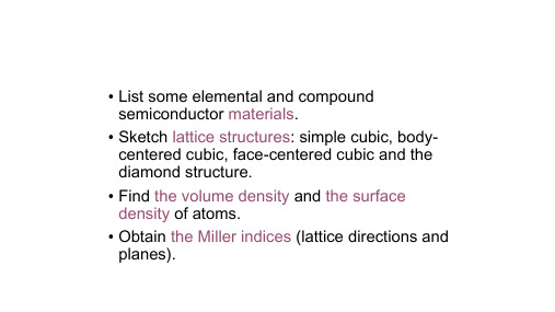
• Discuss carrier drift current density. • Discuss the mechanisms of lattice scattering and impurity scattering. • Define mobility and discuss the temperature and ionized impurity concentration dependence on mobility.
1. Describe carrier drift current density and carrier diffusion current density. Define conductivity and resistivity. What’s the Einstein relationship? 2. Discuss the mechanisms of lattice scattering and impurity scattering. What are the temperature and ionized impurity concentration dependence on mobility? 3. Discuss velocity saturation.
3-Checkpoint • Discuss the concept of allowed and forbidden energy bands in a single crystal both qualitatively and more rigorously from the results of using the Kronig-Penney model. • Discuss the splitting of energy bands in silicon. • Discuss the concept of a hole in terms of the effective mass, covalent bonding and energy bands. • Qualitatively, in terms of energy bands, discuss the difference between metals, insulators, and semiconductors. • Understand the density of states function. • Understand the meaning of the Fermi-Dirac distribution and the Fermi energy.
EPITAXIAL GROWTH SUBSTRATE AND LIGHT-EMITTING ELEM
专利名称:EPITAXIAL GROWTH SUBSTRATE ANDLIGHT-EMITTING ELEMENT USING SAME发明人:SEKI, Takashi,NISHIMURA,Suzushi,TORIYAMA, Shigetaka,TAKAHASHI,Madoka申请号:EP15768215.4申请日:20150326公开号:EP3125312A1公开日:20170201专利内容由知识产权出版社提供专利附图:摘要:An epitaxial growth substrate includes a base member, and a concave-convexpattern having a plurality of concavities and a plurality of convexities and formed on the base member, wherein: each of the plurality of convexities has an elongated shape which extends while winding (waving) in a plane view; and the plurality of convexities in the concave-convex pattern have extending directions, bending directions and lengths which are non-uniform among the plurality of convexities. There are provided an epitaxial growth substrate which can be produced efficiently and which is capable of improving the light-emitting efficiency of a light-emitting element; and a light-emitting element using the epitaxial growth substrate.申请人:JX Nippon Oil & Energy Corporation地址:1-2, Otemachi, 1-chome, Chiyoda-ku Tokyo 100-8162 JP国籍:JP代理机构:Kuhnen & Wacker更多信息请下载全文后查看。
半导体制造技术
Semiconductor Manufacturing Technology半导体制造技术Instructor’s ManualMichael QuirkJulian SerdaCopyright Prentice HallTable of Contents目录OverviewI. Chapter1. Semiconductor industry overview2. Semiconductor materials3. Device technologies—IC families4. Silicon and wafer preparation5. Chemicals in the industry6. Contamination control7. Process metrology8. Process gas controls9. IC fabrication overview10. Oxidation11. Deposition12. Metallization13. Photoresist14. Exposure15. Develop16. Etch17. Ion implant18. Polish19. Test20. Assembly and packagingII. Answers to End-of-Chapter Review QuestionsIII. Test Bank (supplied on diskette)IV. Chapter illustrations, tables, bulleted lists and major topics (supplied on CD-ROM)Notes to Instructors:1)The chapter overview provides a concise summary of the main topics in each chapter.2)The correct answer for each test bank question is highlighted in bold. Test bankquestions are based on the end-of-chapter questions. If a student studies the end-of-chapter questions (which are linked to the italicized words in each chapter), then they will be successful on the test bank questions.2Chapter 1Introduction to the Semiconductor Industry Die:管芯 defective:有缺陷的Development of an Industry•The roots of the electronic industry are based on the vacuum tube and early use of silicon for signal transmission prior to World War II. The first electronic computer, the ENIAC, wasdeveloped at the University of Pennsylvania during World War II.•William Shockley, John Bardeen and Walter Brattain invented the solid-state transistor at Bell Telephone Laboratories on December 16, 1947. The semiconductor industry grew rapidly in the 1950s to commercialize the new transistor technology, with many early pioneers working inSilicon Valley in Northern California.Circuit Integration•The first integrated circuit, or IC, was independently co-invented by Jack Kilby at Texas Instruments and Robert Noyce at Fairchild Semiconductor in 1959. An IC integrates multiple electronic components on one substrate of silicon.•Circuit integration eras are: small scale integration (SSI) with 2 - 50 components, medium scale integration (MSI) with 50 – 5k components, large scale integration (LSI) with 5k to 100kcomponents, very large scale integration (VLSI) with 100k to 1M components, and ultra large scale integration (ULSI) with > 1M components.1IC Fabrication•Chips (or die) are fabricated on a thin slice of silicon, known as a wafer (or substrate). Wafers are fabricated in a facility known as a wafer fab, or simply fab.•The five stages of IC fabrication are:Wafer preparation: silicon is purified and prepared into wafers.Wafer fabrication: microchips are fabricated in a wafer fab by either a merchant chip supplier, captive chip producer, fabless company or foundry.Wafer test: Each individual die is probed and electrically tested to sort for good or bad chips.Assembly and packaging: Each individual die is assembled into its electronic package.Final test: Each packaged IC undergoes final electrical test.•Key semiconductor trends are:Increase in chip performance through reduced critical dimensions (CD), more components per chip (Moore’s law, which predicts the doubling of components every 18-24 months) andreduced power consumption.Increase in chip reliability during usage.Reduction in chip price, with an estimated price reduction of 100 million times for the 50 years prior to 1996.The Electronic Era•The 1950s saw the development of many different types of transistor technology, and lead to the development of the silicon age.•The 1960s were an era of process development to begin the integration of ICs, with many new chip-manufacturing companies.•The 1970s were the era of medium-scale integration and saw increased competition in the industry, the development of the microprocessor and the development of equipment technology. •The 1980s introduced automation into the wafer fab and improvements in manufacturing efficiency and product quality.•The 1990s were the ULSI integration era with the volume production of a wide range of ICs with sub-micron geometries.Career paths•There are a wide range of career paths in semiconductor manufacturing, including technician, engineer and management.2Chapter 2 Characteristics of Semiconductor MaterialsAtomic Structure•The atomic model has three types of particles: neutral neutrons(不带电的中子), positively charged protons(带正电的质子)in the nucleus and negatively charged electrons(带负电的核外电子) that orbit the nucleus. Outermost electrons are in the valence shell, and influence the chemical and physical properties of the atom. Ions form when an atom gains or loses one or more electrons.The Periodic Table•The periodic table lists all known elements. The group number of the periodic table represents the number of valence shell electrons of the element. We are primarily concerned with group numbers IA through VIIIA.•Ionic bonds are formed when valence shell electrons are transferred from the atoms of one element to another. Unstable atoms (e.g., group VIIIA atoms because they lack one electron) easily form ionic bonds.•Covalent bonds have atoms of different elements that share valence shell electrons.3Classifying Materials•There are three difference classes of materials:ConductorsInsulatorsSemiconductors•Conductor materials have low resistance to current flow, such as copper. Insulators have high resistance to current flow. Capacitance is the storage of electrical charge on two conductive plates separated by a dielectric material. The quality of the insulation material between the plates is the dielectric constant. Semiconductor materials can function as either a conductor or insulator.Silicon•Silicon is an elemental semiconductor material because of four valence shell electrons. It occurs in nature as silica and is refined and purified to make wafers.•Pure silicon is intrinsic silicon. The silicon atoms bond together in covalent bonds, which defines many of silicon’s properties. Silicon atoms bond together in set, repeatable patterns, referred to asa crystal.•Germanium was the first semiconductor material used to make chips, but it was soon replaced by silicon. The reasons for this change are:Abundance of siliconHigher melting temperature for wider processing rangeWide temperature range during semiconductor usageNatural growth of silicon dioxide•Silicon dioxide (SiO2) is a high quality, stable electrical insulator material that also serves as a good chemical barrier to protect silicon from external contaminants. The ability to grow stable, thin SiO2 is fundamental to the fabrication of Metal-Oxide-Semiconductor (MOS) devices. •Doping increases silicon conductivity by adding small amounts of other elements. Common dopant elements are from trivalent, p-type Group IIIA (boron) and pentavalent, n-type Group VA (phosphorus, arsenic and antimony).•It is the junction between the n-type and p-type doped regions (referred to as a pn junction) that permit silicon to function as a semiconductor.4Alternative Semiconductor Materials•The alternative semiconductor materials are primarily the compound semiconductors. They are formed from Group IIIA and Group VA (referred to as III-V compounds). An example is gallium arsenide (GaAs).•Some alternative semiconductors come from Group IIA and VIA, referred to as II-VI compounds. •GaAs is the most common III-V compound semiconductor material. GaAs ICs have greater electron mobility, and therefore are faster than ICs made with silicon. GaAs ICs also have higher radiation hardness than silicon, which is better for space and military applications. The primary disadvantage of GaAs is the lack of a natural oxide.5Chapter 3Device TechnologiesCircuit Types•There are two basic types of circuits: analog and digital. Analog circuits have electrical data that varies continuously over a range of voltage, current and power values. Digital circuits have operating signals that vary about two distinct voltage levels – a high and a low.Passive Component Structures•Passive components such as resistors and capacitors conduct electrical current regardless of how the component is connected. IC resistors are a passive component. They can have unwanted resistance known as parasitic resistance. IC capacitor structures can also have unintentional capacitanceActive Component Structures•Active components, such as diodes and transistors can be used to control the direction of current flow. PN junction diodes are formed when there is a region of n-type semiconductor adjacent to a region of p-type semiconductor. A difference in charge at the pn junction creates a depletion region that results in a barrier voltage that must be overcome before a diode can be operated. A bias voltage can be configured to have a reverse bias, with little or no conduction through the diode, or with a forward bias, which permits current flow.•The bipolar junction transistor (BJT) has three electrodes and two pn junctions. A BJT is configured as an npn or pnp transistor and biased for conduction mode. It is a current-amplifying device.6• A schottky diode is formed when metal is brought in contact with a lightly doped n-type semiconductor material. This diode is used in faster and more power efficient BJT circuits.•The field-effect transistor (FET), a voltage-amplifying device, is more compact and power efficient than BJT devices. A thin gate oxide located between the other two electrodes of the transistor insulates the gate on the MOSFET. There are two categories of MOSFETs, nMOS (n-channel) and pMOS (p-channel), each which is defined by its majority current carriers. There is a biasing scheme for operating each type of MOSFET in conduction mode.•For many years, nMOS transistors have been the choice of most IC manufacturers. CMOS, with both nMOS and pMOS transistors in the same IC, has been the most popular device technology since the early 1980s.•BiCMOS technology makes use of the best features of both CMOS and bipolar technology in the same IC device.•Another way to categorize FETs is in terms of enhancement mode and depletion mode. The major different is in the way the channels are doped: enhancement-mode channels are doped opposite in polarity to the source and drain regions, whereas depletion mode channels are doped the same as their respective source and drain regions.Latchup in CMOS Devices•Parasitic transistors can create a latchup condition(???????) in CMOS ICs that causes transistors to unintentionally(无心的) turn on. To control latchup, an epitaxial layer is grown on the wafer surface and an isolation barrier(隔离阻障)is placed between the transistors. An isolation layer can also be buried deep below the transistors.Integrated Circuit Productsz There are a wide range of semiconductor ICs found in electrical and electronic products. This includes the linear IC family, which operates primarily with anal3og circuit applications, and the digital IC family, which includes devices that operate with binary bits of data signals.7Chapter 4Silicon and Wafer Preparation8z Semiconductor-Grade Silicon•The highly refined silicon used for wafer fabrication is termed semiconductor-grade silicon (SGS), and sometimes referred to as electronic-grade silicon. The ultra-high purity of semiconductor-grade silicon is obtained from a multi-step process referred to as the Siemens process.Crystal Structure• A crystal is a solid material with an ordered, 3-dimensional pattern over a long range. This is different from an amorphous material that lacks a repetitive structure.•The unit cell is the most fundamental entity for the long-range order found in crystals. The silicon unit cell is a face-centered cubic diamond structure. Unit cells can be organized in a non-regular arrangement, known as a polycrystal. A monocrystal are neatly arranged unit cells.Crystal Orientation•The orientation of unit cells in a crystal is described by a set of numbers known as Miller indices.The most common crystal planes on a wafer are (100), (110), and (111). Wafers with a (100) crystal plane orientation are most common for MOS devices, whereas (111) is most common for bipolar devices.Monocrystal Silicon Growth•Silicon monocrystal ingots are grown with the Czochralski (CZ) method to achieve the correct crystal orientation and doping. A CZ crystal puller is used to grow the silicon ingots. Chunks of silicon are heated in a crucible in the furnace of the puller, while a perfect silicon crystal seed is used to start the new crystal structure.• A pull process serves to precisely replicate the seed structure. The main parameters during the ingot growth are pull rate and crystal rotation. More homogeneous crystals are achieved with a magnetic field around the silicon melt, known as magnetic CZ.•Dopant material is added to the melt to dope the silicon ingot to the desired electrical resistivity.Impurities are controlled during ingot growth. A float-zone crystal growth method is used toachieve high-purity silicon with lower oxygen content.•Large-diameter ingots are grown today, with a transition underway to produce 300-mm ingot diameters. There are cost benefits for larger diameter wafers, including more die produced on a single wafer.Crystal Defects in Silicon•Crystal defects are interruptions in the repetitive nature of the unit cell. Defect density is the number of defects per square centimeter of wafer surface.•Three general types of crystal defects are: 1) point defects, 2) dislocations, and 3) gross defects.Point defects are vacancies (or voids), interstitial (an atom located in a void) and Frenkel defects, where an atom leaves its lattice site and positions itself in a void. A form of dislocation is astacking fault, which is due to layer stacking errors. Oxygen-induced stacking faults are induced following thermal oxidation. Gross defects are related to the crystal structure (often occurring during crystal growth).Wafer Preparation•The cylindrical, single-crystal ingot undergoes a series of process steps to create wafers, including machining operations, chemical operations, surface polishing and quality checks.•The first wafer preparation steps are the shaping operations: end removal, diameter grinding, and wafer flat or notch. Once these are complete, the ingot undergoes wafer slicing, followed by wafer lapping to remove mechanical damage and an edge contour. Wafer etching is done to chemically remove damage and contamination, followed by polishing. The final steps are cleaning, wafer evaluation and packaging.Quality Measures•Wafer suppliers must produce wafers to stringent quality requirements, including: Physical dimensions: actual dimensions of the wafer (e.g., thickness, etc.).Flatness: linear thickness variation across the wafer.Microroughness: peaks and valleys found on the wafer surface.Oxygen content: excessive oxygen can affect mechanical and electrical properties.Crystal defects: must be minimized for optimum wafer quality.Particles: controlled to minimize yield loss during wafer fabrication.Bulk resistivity(电阻系数): uniform resistivity from doping during crystal growth is critical. Epitaxial Layer•An epitaxial layer (or epi layer) is grown on the wafer surface to achieve the same single crystal structure of the wafer with control over doping type of the epi layer. Epitaxy minimizes latch-up problems as device geometries continue to shrink.Chapter 5Chemicals in Semiconductor FabricationEquipment Service Chase Production BayChemical Supply Room Chemical Distribution Center Holding tank Chemical drumsProcess equipmentControl unit Pump Filter Raised and perforated floorElectronic control cablesSupply air ductDual-wall piping for leak confinement PumpFilterChemical control and leak detection Valve boxes for leak containment Exhaust air ductStates of Matter• Matter in the universe exists in 3 basic states (宇宙万物存在着三种基本形态): solid, liquid andgas. A fourth state is plasma.Properties of Materials• Material properties are the physical and chemical characteristics that describe its unique identity.• Different properties for chemicals in semiconductor manufacturing are: temperature, pressure andvacuum, condensation, vapor pressure, sublimation and deposition, density, surface tension, thermal expansion and stress.Temperature is a measure of how hot or cold a substance is relative to another substance. Pressure is the force exerted per unit area. Vacuum is the removal of gas molecules.Condensation is the process of changing a gas into a liquid. Vaporization is changing a liquidinto a gas.Vapor pressure is the pressure exerted by a vapor in a closed container at equilibrium.Sublimation is the process of changing a solid directly into a gas. Deposition is changing a gas into a solid.Density is the mass of a substance divided by its volume.Surface tension of a liquid is the energy required to increase the surface area of contact.Thermal expansion is the increase in an object’s dimension due to heating.Stress occurs when an object is exposed to a force.Process Chemicals•Semiconductor manufacturing requires extensive chemicals.• A chemical solution is a chemical mixture. The solvent is the component of the solution present in larger amount. The dissolved substances are the solutes.•Acids are solutions that contain hydrogen and dissociate in water to yield hydronium ions. A base is a substance that contains the OH chemical group and dissociates in water to yield the hydroxide ion, OH-.•The pH scale is used to assess the strength of a solution as an acid or base. The pH scale varies from 0 to 14, with 7 being the neutral point. Acids have pH below 7 and bases have pH values above 7.• A solvent is a substance capable of dissolving another substance to form a solution.• A bulk chemical distribution (BCD) system is often used to deliver liquid chemicals to the process tools. Some chemicals are not suitable for BCD and instead use point-of-use (POU) delivery, which means they are stored and used at the process station.•Gases are generally categorized as bulk gases or specialty gases. Bulk gases are the relatively simple gases to manufacture and are traditionally oxygen, nitrogen, hydrogen, helium and argon.The specialty gases, or process gases, are other important gases used in a wafer fab, and usually supplied in low volume.•Specialty gases are usually transported to the fab in metal cylinders.•The local gas distribution system requires a gas purge to flush out undesirable residual gas. Gas delivery systems have special piping and connections systems. A gas stick controls the incoming gas at the process tool.•Specialty gases may be classified as hydrides, fluorinated compounds or acid gases.Chapter 6Contamination Control in Wafer FabsIntroduction•Modern semiconductor manufacturing is performed in a cleanroom, isolated from the outside environment and contaminants.Types of contamination•Cleanroom contamination has five categories: particles, metallic impurities, organic contamination, native oxides and electrostatic discharge. Killer defects are those causes of failure where the chip fails during electrical test.Particles: objects that adhere to a wafer surface and cause yield loss. A particle is a killer defect if it is greater than one-half the minimum device feature size.Metallic impurities: the alkali metals found in common chemicals. Metallic ions are highly mobile and referred to as mobile ionic contaminants (MICs).Organic contamination: contains carbon, such as lubricants and bacteria.Native oxides: thin layer of oxide growth on the wafer surface due to exposure to air.Electrostatic discharge (ESD): uncontrolled transfer of static charge that can damage the microchip.Sources and Control of Contamination•The sources of contamination in a wafer fab are: air, humans, facility, water, process chemicals, process gases and production equipment.Air: class number designates the air quality inside a cleanroom by defining the particle size and density.Humans: a human is a particle generator. Humans wear a cleanroom garment and follow cleanroom protocol to minimize contamination.Facility: the layout is generally done as a ballroom (open space) or bay and chase design.Laminar airflow with air filtering is used to minimize particles. Electrostatic discharge iscontrolled by static-dissipative materials, grounding and air ionization.Ultrapure deiniozed (DI) water: Unacceptable contaminants are removed from DI water through filtration to maintain a resistivity of 18 megohm-cm. The zeta potential represents a charge on fine particles in water, which are trapped by a special filter. UV lamps are used for bacterial sterilization.Process chemicals: filtered to be free of contamination, either by particle filtration, microfiltration (membrane filter), ultrafiltration and reverse osmosis (or hyperfiltration).Process gases: filtered to achieve ultraclean gas.Production equipment: a significant source of particles in a fab.Workstation design: a common layout is bulkhead equipment, where the major equipment is located behind the production bay in the service chase. Wafer handling is done with robotic wafer handlers. A minienvironment is a localized environment where wafers are transferred on a pod and isolated from contamination.Wafer Wet Cleaning•The predominant wafer surface cleaning process is with wet chemistry. The industry standard wet-clean process is the RCA clean, consisting of standard clean 1 (SC-1) and standard clean 2 (SC-2).•SC-1 is a mixture of ammonium hydroxide, hydrogen peroxide and DI water and capable of removing particles and organic materials. For particles, removal is primarily through oxidation of the particle or electric repulsion.•SC-2 is a mixture of hydrochloric acid, hydrogen peroxide and DI water and used to remove metals from the wafer surface.•RCA clean has been modified with diluted cleaning chemistries. The piranha cleaning mixture combines sulfuric acid and hydrogen peroxide to remove organic and metallic impurities. Many cleaning steps include an HF last step to remove native oxide.•Megasonics(兆声清洗) is widely used for wet cleaning. It has ultrasonic energy with frequencies near 1 MHz. Spray cleaning will spray wet-cleaning chemicals onto the wafer. Scrubbing is an effective method for removing particles from the wafer surface.•Wafer rinse is done with overflow rinse, dump rinse and spray rinse. Wafer drying is done with spin dryer or IPA(异丙醇) vapor dry (isopropyl alcohol).•Some alternatives to RCA clean are dry cleaning, such as with plasma-based cleaning, ozone and cryogenic aerosol cleaning.Chapter 7Metrology and Defect InspectionIC Metrology•In a wafer fab, metrology refers to the techniques and procedures for determining physical and electrical properties of the wafer.•In-process data has traditionally been collected on monitor wafers. Measurement equipment is either stand-alone or integrated.•Yield is the percent of good parts produced out of the total group of parts started. It is an indicator of the health of the fabrication process.Quality Measures•Semiconductor quality measures define the requirements for specific aspects of wafer fabrication to ensure acceptable device performance.•Film thickness is generally divided into the measurement of opaque film or transparent film. Sheet resistance measured with a four-point probe is a common method of measuring opaque films (e.g., metal film). A contour map shows sheet resistance deviations across the wafer surface.•Ellipsometry is a nondestructive, noncontact measurement technique for transparent films. It works based on linearly polarized light that reflects off the sample and is elliptically polarized.•Reflectometry is used to measure a film thickness based on how light reflects off the top and bottom surface of the film layer. X-ray and photoacoustic technology are also used to measure film thickness.•Film stress is measured by analyzing changes in the radius of curvature of the wafer. Variations in the refractive index are used to highlight contamination in the film.•Dopant concentration is traditionally measured with a four-point probe. The latest technology is the thermal-wave system, which measures the lattice damage in the implanted wafer after ion implantation. Another method for measuring dopant concentration is spreading resistance probe. •Brightfield detection is the traditional light source for microscope equipment. An optical microscope uses light reflection to detect surface defects. Darkfield detection examines light scattered off defects on the wafer surface. Light scattering uses darkfield detection to detectsurface particles by illuminating the surface with laser light and then using optical imaging.•Critical dimensions (CDs) are measured to achieve precise control over feature size dimensions.The scanning electron microscope is often used to measure CDs.•Conformal step coverage is measured with a surface profiler that has a stylus tip.•Overlay registration measures the ability to accurately print photoresist patterns over a previously etched pattern.•Capacitance-voltage (C-V) test is used to verify acceptable charge conditions and cleanliness at the gate structure in a MOS device.Analytical Equipment•The secondary-ion mass spectrometry (SIMS) is a method of eroding a wafer surface with accelerated ions in a magnetic field to analyze the surface material composition.•The atomic force microscope (AFM) is a surface profiler that scans a small, counterbalanced tip probe over the wafer to create a 3-D surface map.•Auger electron spectroscopy (AES) measures composition on the wafer surface by measuring the energy of the auger electrons. It identifies elements to a depth of about 2 nm. Another instrument used to identify surface chemical species is X-ray photoelectron spectroscopy (XPS).•Transmission electron microscopy (TEM) uses a beam of electrons that is transmitted through a thin slice of the wafer. It is capable of quantifying very small features on a wafer, such as silicon crystal point defects.•Energy-dispersive spectrometer (EDX) is a widely used X-ray detection method for identifying elements. It is often used in conjunction with the SEM.• A focused ion beam (FIB) system is a destructive technique that focuses a beam of ions on the wafer to carve a thin cross section from any wafer area. This permits analysis of the wafermaterial.Chapter 8Gas Control in Process ChambersEtch process chambers••The process chamber is a controlled vacuum environment where intended chemical reactions take place under controlled conditions. Process chambers are often configured as a cluster tool. Vacuum•Vacuum ranges are low (rough) vacuum, medium vacuum, high vacuum and ultrahigh vacuum (UHV). When pressure is lowered in a vacuum, the mean free path(平均自由行程) increases, which is important for how gases flow through the system and for creating a plasma.Vacuum Pumps•Roughing pumps are used to achieve a low to medium vacuum and to exhaust a high vacuum pump. High vacuum pumps achieve a high to ultrahigh vacuum.•Roughing pumps are dry mechanical pumps or a blower pump (also referred to as a booster). Two common high vacuum pumps are a turbomolecular (turbo) pump and cryopump. The turbo pump is a reliable, clean pump that works on the principle of mechanical compression. The cryopump isa capture pump that removes gases from the process chamber by freezing them.。
Strain engineering in semiconductor materials

Strain engineering in semiconductormaterials现代半导体技术发展迅猛,从传统硅晶体到新型半导体材料的转变,带来了新的机遇和挑战。
半导体材料的性能往往决定着电子元器件的性能和发展方向。
随着技术的不断革新和工艺的不断优化,人们对半导体材料的研究和应用也越来越精深。
Strain engineering(应变工程)被广泛地应用于半导体材料中,通过引入外界压力或拉力,改变材料的结构和性能。
应变工程的基本思想是通过对半导体材料施加压力或拉伸,使晶体在不改变材料本身化学性质的情况下,产生局部晶格畸变,从而影响材料的能带结构,进而改变材料的电学、光学等物理性质。
在半导体器件的制造过程中,常用的方法是在硅、锗或III-V族半导体(如GaAs、InP、GaN等)基板上生长薄膜,以制造半导体器件。
应变工程技术可以通过调整薄膜的晶格匹配度,实现材料性能的升级和优化。
具体而言,在硅基板上生长薄膜时,通过在生长过程中施加压力或拉伸,可以使薄膜晶格与基板之间出现畸变,从而产生晶格应变。
晶格应变的发生,会导致半导体材料的能带结构发生变化,从而影响半导体的发光、导电等特性。
相对于晶体缺陷等其它制备方法,应变工程是一种较为可控的方法,具有较强的实用性和可操作性。
应用应变工程技术的最主要目的就是改变半导体的能带结构,以从根本上影响其性能。
例如,通过在硅基板上生长薄膜,我们可以制造出不同的红外、紫外、可见光等截然不同的光学设备,并应用于太阳能电池、激光器等领域。
此外,应变工程技术也可以被广泛应用在其他材料上,如硼氮化镓等III-V族半导体材料,甚至用于奇特的石墨烯单晶体制备。
在硼氮化镓等材料中,因为制造过程材料间的晶格匹配程度通常不高,可以通过应变工程技术等手段,实现晶格对半导体性能的调控,到达更高的性能要求。
总的来说,半导体材料在今后的发展中还需要通过各种高深技术的应用,实现物理属性的升级和优化,以促进整个电子工业的进步。
微电子专业英语翻译

当超量载流子被导入一个直接禁带半导体时,电子与空穴直接复合的几率 较高,这是因为导带的底部与价带的顶端位于同一线上,因此在禁带间跃 迁时,无需额外的动量。直接复合率R应正比于导带中含有的电子数目及 价带中含有的空穴数目。也就是 R=βnp 。其中β为比例常数。
As discussed previously, in thermal equilibrium the recombination rate must be balanced by the generation rate . Therefore , for an n-type semiconductor, we have Gth=Rth=βn no p no where nno and pno represent electron and hole densities in an n-type semiconductor at thermal equilibrium. When we shine a light on the semiconductor to produce electron-hole pairs at a rate GL(Fig.2.11(b)), the carrier concentrations are above their equilibrium values.
当超量载流子被导入一个直接禁带半导体时电子与空穴直接复合的几率较高这是因为导带的底部与价带的顶端位于同一线上因此在禁带间跃迁时无需额外的动量
2.5 Generation and Recombination Processes 载流子产生与复合过程
3. Characteristics of Diodes二极管特性 3.1 Introduction介绍
当电子从导带向下移到价带, 一个电子 - 空穴对消失。这 种反向过程称为复合,并以 复 合 率 Rth 表 示 , 如 图 2.11 ( a )所示。在热平衡状态 下,产生速率 Gth 必定等于 复合率 Rth ,所以载流子浓 度维持常数,且维持 pn=ni2 的状况。
Liquid-phaseepit...
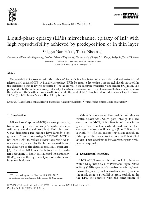
Journal of Crystal Growth 203(1999)459}463Liquid-phase epitaxy (LPE)microchannel epitaxy of InP with high reproducibility achieved by predeposition of In thin layerShigeya Naritsuka *,Tatau NishinagaDepartment of Electronics Engineering,Graduate School of Engineering,The Uni v ersity of Tokyo,7-3-1Hongo,Bunkyo-ku,Tokyo 113,JapanReceived 18November 1998;accepted 25February 1999Communicated by G.B.StringfellowAbstractThe wettability of a solution with the surface of line seeds is a key factor to improve the yield and uniformity of microchannel epitaxy (MCE)by liquid phase epitaxy (LPE).To improve the wetting,a special technique is proposed.In this technique,a thin In layer is deposited before the growth on the substrate with narrow line seeds in SiOmask.Thepredeposited In "lm in the seed area greatly helps the solution to contact with the surface inside the line seeds even when the width and the length are very small.As a result,the yield of MCE has been drastically increased up to almost 100%. 1999Elsevier Science B.V.All rights reserved.Keywords:Microchannel epitaxy;Indium phosphide;High reproducibility;Wetting;Predeposition;Liquid-phase epitaxy1.IntroductionMicrochannel epitaxy (MCE)is a very promising technique to provide atomically #at epitaxial layers with very few dislocations [1}5].Both InP and GaAs dislocation-free regions have already been grown on Si substrates using MCE [6}9].MCE is not only useful to reduce dislocations but also to release stress,caused by the lattice mismatch and the di !erence in the thermal expansion coe $cient [7].Therefore,MCE is suitable to solve the prob-lems occurring in highly mismatched heteroepitaxy (HM ),such as the high density of dislocations and large residual stress.*Corresponding author.Fax:#81-3-5684-3947.E-mail address:nari @ee.t.u-tokyo.ac.jp (S.Naritsuka)Although a narrower line seed is desirable to reduce dislocations which pass through the line seed area in MCE,it is often found there is no growth from the line seeds of small widths.For example,line seeds with a length (¸)of 200 m and a width (=)of 3 m give no InP MCE growth.In this report,the reason for the poor yield is studied at "rst.Then,a technique for overcoming the prob-lem is proposed.2.Experimental procedureMCE of InP was carried out on InP substrates with a SiOmask by a conventional liquid phaseepitaxy (LPE)system of a horizontal sliding boat.Before the growth,the line windows were opened in the mask using a photolithographic technique.In the LPE,the solution with the composition of0022-0248/99/$-see front matter 1999Elsevier Science B.V.All rights reserved.PII:S 0022-0248(99)00136-0Fig.1.(a)Photomicrograph of a substrate surface after conventional MCE process and (b)schematic illustration of the speculated cross section of the solution and the substrate with line seeds during MCE growth.In :Sn "25:75(in weight)was employed and the solution was kept in contact with an InP source crystal for 1h at a saturation temperature of 5503C to complete saturation.In the typical growth pro-cess,the temperature was reduced by 13C at a rate of 0.13C/min.Then the melt was brought into con-tact with the substrate and MCE of InP was started.The typical growth time was chosen as 1h.The experimental details were described in our pre-vious papers [5,6].3.Results and discussionFig.1a shows a microphotograph of a substrate after MCE by conventional method.Here,lineseeds with ¸of 70,90and 140 m and =of 3 m were employed.The "gure shows that no MCE layer was grown from the line seeds.Moreover,no surface morphology showing the growth was ob-served in the line seed areas.This observation sug-gests that the solution has no contact with the surfaces in the line seed area,as schematically shown in Fig.1b.The large surface tension of the solution might be the origin of preventing the contact.To con "rm this,the following experiment was carried out.A mask with a wide opening,as shown in Fig.2a,was used to make the complete wetting of the solution in this area.The direct connection of the open area to the line seeds was employed to keep the continuos wetting from the wide area to460S.Naritsuka,T.Nishinaga /Journal of Crystal Growth 203(1999)459}463Fig.2.(a)Schematic illustration of a special mask with a large wetting area and(b)MCE layer grown from the mask given in(a).the line seeds.MCE layers grown with this mask are shown in Fig.2b.It was found that the MCE layers perfectly cover all line seeds even in the case when the width of the line seeds is less than2 m. This result shows that the wetting is the key factor to govern the yield of MCE.However,the mask of this type cannot be used for practical use because isolated MCE layers are usually required.It is quite di$cult for the solution to wet the small seed area due to the surface tension as dis-cussed before.To overcome this problem,an In thin layer was deposited on the substrate before the growth,as illustrated in Fig.3a,in order to allow for the solution to easily contact with the line seeds in the very beginning of the growth.MCE layers thus grown are shown in Fig.3b.The thickness ofthe In layer was chosen about5800A.Although thewidth of the line seeds was only2.5 m in this case,it is seen in the"gure that all the line seeds wereperfectly covered with the grown InP MCE layers.The MCE layers were grown even on the line seedswith a length of less than2 m,as shown in Fig.3c.Here,a pin-hole in the SiO mask has worked as a seed for MCE.A series of MCE layers weregrown from aligned circular holes with small dia-meter,which had been made from an imperfectphotolithography of a straight line seed.This indi-cates that by this method the wetting of the solu-tion can be accomplished even in very small areaslike pin-holes.S.Naritsuka,T.Nishinaga/Journal of Crystal Growth203(1999)459}463461Fig.3.(a)Schematic illustration of MCE substrate after the deposition of a thin In layer.MCE layers grown(b)from line seeds and(c) from unintentionally introduced pin holes,after In deposition.4.ConclusionsThe wetting of the solution with the line seeds is a key factor governing the yield of MCE.It was found that the deposition of a thin In layer before growth has greatly improved the wetting and,as a result,the yield of MCE has been increased up to almost100%.AcknowledgementsThe authors would like to express thanks to Dr. M.Tanaka for useful discussions.This work was supported by a Grant-in-Aid for Scienti"c Re-search(B)`Growth of dislocation-free GaAs layers on Si substrates by microchannel epitaxy and fabri-cation of laser diodes a No.10555119from the462S.Naritsuka,T.Nishinaga/Journal of Crystal Growth203(1999)459}463Ministry of Education,Science,Sports and Culture and by JSPS Research for the Future Program in the Area of Atomic-Scale Surface and Interface Dynamic under the project of`Self-assembling of Nanostructures and Its Control a.References[1]T.Nishinaga,T.Nakano,S.Zhang,Jpn.J.Appl.Phys.27(1988)L964.[2]Y.Suzuki,T.Nishinaga,Jpn.J.Appl.Phys.28(1989)440.[3]Y.Suzuki,T.Nishinaga,J.Crystal Growth99(1990)229.[4]S.Zhang,T.Nishinaga,J.Crystal Growth99(1990)292.[5]S.Naritsuka,T.Nishinaga,J.Crystal Growth146(1995)314.[6]S.Naritsuka,T.Nishinaga,M.Tachikawa,H.Mori,Jpn.J.Appl.Phys.34(1995)L1432.[7]S.Naritsuka,T.Nishinaga,J.Crystal Growth174(1997)622.[8]Y.Ujiie,T.Nishinaga,Jpn.J.Appl.Phys.28(1989)L337.[9]S.Sakawa,T.Nishinaga,Jpn.J.Appl.Phys.31(1992)L359.S.Naritsuka,T.Nishinaga/Journal of Crystal Growth203(1999)459}463463。
表面等离子体共振显微术的空间分辨力
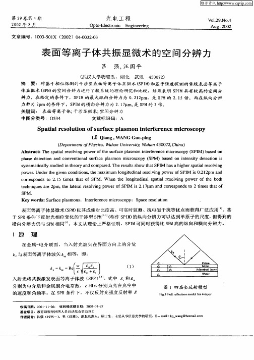
表 面 等 离 子 体 振 术 的 空 间分 辨 力 共 显微
吕 强 , 国平 汪
( 汉 大 学 物 理 系 ,湖 北 武 武汉 4 07) 3 0 2
摘
要 :对基 于相位探 测的干 涉型表 面等 离子体 显微术 (P M 和基 于强度探 测的 常规 表 面等 离子 S I)
体显微 术 (P ) S M 的空间分辨 力进行 了较 系统的理论研 究和比较 ,结 果表 明 S I P M具有较 高的空间分 辨 力 。在给 定的条件 下 ,S I P M的最 大纵 向分辨 力为 0 2 m,是 SM的 2 1 倍 。 而在纵 向分辨 . 1p 2 P .5
于 S R条 件 下 反 射 光 相 位 变 化 的 干 涉 型 S M 。( 作 S I ) P P 瞠。 称 “ P M 的纵 向 分 辨 力 可 以达 到 单 原 子 的 尺 度 , 得 到 的 但 横 向 分 辨 力 仍 与 S M相 同 。 本 文 从 理 论 上 严 格 证 明 ,S I P P M可 同 时 获得 比 S M高 的 纵 向和 横 向分 辨 力 。 P
L JQin WANG o pn I a g, Gu - ig
( p r n h sc, u a n vri , h n4 0 7 , ia De a t tfP y is W h nU ie sy Wu a 3 0 2Chn ) me o t
Ab ta t T es ail eovn o r fh u a epamo tr rn emir so y( P M ) ae n sr c: h p t s ligp we es r c ls ni e ee c co c p S I b sdo ar ot f n f p ae d tcin a d c n e t n ls r c ls n m co c p (P ) a e n it st ee t n i h s ee t n o v ni a u a e pamo r so y S M b s d o ne i d t i s o o f i n y co
- 1、下载文档前请自行甄别文档内容的完整性,平台不提供额外的编辑、内容补充、找答案等附加服务。
- 2、"仅部分预览"的文档,不可在线预览部分如存在完整性等问题,可反馈申请退款(可完整预览的文档不适用该条件!)。
- 3、如文档侵犯您的权益,请联系客服反馈,我们会尽快为您处理(人工客服工作时间:9:00-18:30)。
Epitaxial interfaces in semi-crystalline polymers and their applications
J. P E T E R M A N N , G. BROZA, U. RIECK, A. K A W A G U C H I *
Figure 1 Transmission electron micrograph o f a lamellar PP substrate film. The molecular direction is indicated by an arrow and the electron diffraction pattern is inserted.
PE. 0.5pm
J J -I
(Y
Figure 3 Schematic sketch of the peeling experiment. The arrows within the PP films denote the molecular directions.
The samples for the mechanical tests were prepared as follows: uniaxially oriented films of hot-drawn PP were cross-piled with a 200 nm thin PE film in between, heated in a hot press for 5 min at 155 ° C and cooled to room temperature. The adherence of the cross-piled films was tested in a 180 ° peel-test using a Zwick 1445 tensile testing machine. Fig. 3 shows the experimental arrangement for the test. The sandwiched layered structures were produced as indicated in Fig. 4. The solutions of 0.5% PP and PE in xylene were poured on to two separately heated glass slides. After evaporation of the solvent, a motor driven cylinder was touched on to both glass slides, lifted up and was able to wind up very thin PP and PE-films simultaneously. Again, the films were 50 nm thick and highly oriented. After about 1000 turns of
Polymer and Composite Group, Technical University Hamburg-Harburg, Harburger Schlosstrasse 20, 2100 Hamburg 90, FGR
The epitaxial crystallization of polyethylene (PE) on uniaxially oriented polypropylene is investigated, Mechanical tests indicate that the epitaxial interfaces have strong adherence.
100 kV.
Fig. 1 shows a transmission electron micrograph of a PP-substrate film prepared as described above. The films had a lamellar morphology and a high crystalline fibre texture, as can be estimated from the electron diffraction patterns, inserted into the micrograph. The polymer films used for the layers were solution cast on to hot orthophosphoric acid [10]. In Fig. 2 a layer-film from HDPE is shown. Again, the films were cut into pieces and put on top of the substrate films. Substrate and layers were heated subsequently to 155°C (above Tm of PE but below T~ of PP) and cooled at varying rates to room temper/(t-ure_ The films containing paraffin as the layers were heated to 80°C and subsequently cooled.
Figure 2 Transmission electron microglTaph of a spherulitic PE film,
as used for the layered film. Inserted is the electron diffraction pattern.
*Present address: Institute for Chemical Research, Kyoto University, Uji, Kyoto Fu 611, Japan.
Figure 5 Transmission electron micrographs of epitaxially crystallized HDPE. The molecular directions o f the PP-substrates are horizontal.
(a) Cooling rate I°C min -1 , (b) cooling rate 10°C min 1, (c) cooling rate 100°C min -1 , (d) rapid quenching into ice-water.
0022-2461/87 $03.00 + .12 © 1987 Chapman and Hall Ltd.
1477
C/
take-up roller
PE- melt film
heating prates
PP- melt film
Figure 4 Schematic sketch for the preparation of the layered films.
1478
Figure 6 Electron diffraction patterns from (a) the epitaxial morphologies, and (b) the rapidly que e n t a l p r o c e d u r e
The materials used for the experiments were polypropylene, type PPN from Hrchst AG, polyethylene, type Lupolen 6021 DX (HDPE) and 1810 D (LDPE) from BASF AG and paraffin (n-C28H58) from Merck. Thin oriented substrate films were prepared according to the method of Petermann and Gohil [7]: a small amount of a 0.5% solution of the polymer (PP or PE) in xylene was poured on a hot glass slide where the
1. Introduction
Recently, it was reported that a number of polymers crystallize epitaxially on to polymeric substrates [1-6]. The work of Lotz and Wittmann [4], in particular, demonstrated that the side groups of helical polyolefins (polypropylene, polybutene-l) possess crystallographic interfaces in which the side groups form straight rows along which linear zig-zag chains can well align, and leading to distinct orientation relationships between the lattices of the helical and zig-zag molecules. In the present work further detailed experiments on the epitaxial crystallization of polyethylene (PE) on to uniaxially oriented polypropylene (PP) were carried out. The influence of epitaxial interfaces on the adhesion of polymer laminates and the mechanical properties of sandwiched layers containing epitaxial interfaces are also reported. solvent was allowed to evaporate. The remaining thin polymer film was then picked up on a motor driven cylinder, at a wind-up speed of 20cmsec -1. The resulting thin polymer films were about 50 nm thick and highly oriented in the drawing direction. Oriented PP films containing the/?-modification where crystallized in a strong temperature gradient (200° C mm -1) by zone solidification with a solidification rate of 5 #m min-1 [8, 9]. The films were cut into 3 x 3 mm 2 pieces, floated on to distilled water and mounted on TEM grids. The materials were investigated using a Philips EM-400 T electron microscope operated at