DMBT8050 datasheet
kmps8050d 三极管

SS8050NPN Epitaxial Silicon TransistorAbsolute Maximum Ratings T a =25°C unless otherwise notedElectrical Characteristics T a =25°C unless otherwise notedh FE ClassificationSymbol ParameterRatings Units V CBO Collector-Base Voltage 40V V CEO Collector-Emitter Voltage 25V V EBO Emitter-Base Voltage 6V I C Collector Current1.5A P C Collector Power Dissipation 1W T J Junction Temperature 150°C T STGStorage Temperature-65 ~ 150°CSymbol ParameterTest Condition Min.Typ.Max.Units BV CBO Collector-Base Breakdown Voltage I C =100µA, I E =040V BV CEO Collector-Emitter Breakdown Voltage I C =2mA, I B =025V BV EBO Emitter-Base Breakdown Voltage I E =100µA, I C =06V I CBO Collector Cut-off Current V CB =35V, I E =0100nA I EBO Emitter Cut-off Current V EB =6V, I C =0100nAh FE1h FE2h FE3DC Current GainV CE =1V, I C =5mA V CE =1V, I C =100mA V CE =1V, I C =800mA 458540135160110300V CE (sat)Collector-Emitter Saturation Voltage I C =800mA, I B =80mA 0.280.5V V BE (sat)Base-Emitter Saturation Voltage I C =800mA, I B =80mA 0.98 1.2V V BE (on)Base-Emitter On Voltage V CE =1V, I C =10mA 0.661V C ob Output CapacitanceV CB =10V, I E =0f=1MHz9.0pF f TCurrent Gain Bandwidth ProductV CE =10V, I C =50mA100190MHzClassificationB C D h FE285 ~ 160120 ~ 200160 ~ 300SS80502W Output Amplifier of Portable Radios in Class B Push-pull Operation.•Complimentary to SS8550•Collector Current: I C =1.5A•Collector Power Dissipation: P C =2W (T C =25°C)1. Emitter2. Base3. CollectorTO-921SS8050SS8050TRADEMARKSThe following are registered and unregistered trademarks Fairchild Semiconductor owns or is authorized to use and is not intended to be an exhaustive list of all such trademarks.DISCLAIMERFAIRCHILD SEMICONDUCTOR RESERVES THE RIGHT TO MAKE CHANGES WITHOUT FURTHER NOTICE TO ANY PRODUCTS HEREIN TO IMPROVE RELIABILITY, FUNCTION OR DESIGN. FAIRCHILD DOES NOT ASSUME ANY LIABILITY ARISING OUT OF THE APPLICATION OR USE OF ANY PRODUCT OR CIRCUIT DESCRIBED HEREIN;NEITHER DOES IT CONVEY ANY LICENSE UNDER ITS PATENT RIGHTS, NOR THE RIGHTS OF OTHERS.LIFE SUPPORT POLICYFAIRCHILD’S PRODUCTS ARE NOT AUTHORIZED FOR USE AS CRITICAL COMPONENTS IN LIFE SUPPORT DEVICES OR SYSTEMS WITHOUT THE EXPRESS WRITTEN APPROVAL OF FAIRCHILD SEMICONDUCTOR CORPORATION.As used herein:1. Life support devices or systems are devices or systems which, (a) are intended for surgical implant into the body,or (b) support or sustain life, or (c) whose failure to perform when properly used in accordance with instructions for use provided in the labeling, can be reasonably expected to result in significant injury to the user.2. A critical component is any component of a life support device or system whose failure to perform can be reasonably expected to cause the failure of the life support device or system, or to affect its safety or effectiveness.PRODUCT STATUS DEFINITIONS Definition of TermsDatasheet Identification Product Status DefinitionAdvance InformationFormative or In Design This datasheet contains the design specifications for product development. Specifications may change in any manner without notice.PreliminaryFirst ProductionThis datasheet contains preliminary data, andsupplementary data will be published at a later date.Fairchild Semiconductor reserves the right to make changes at any time without notice in order to improve design.No Identification Needed Full ProductionThis datasheet contains final specifications. Fairchild Semiconductor reserves the right to make changes at any time without notice in order to improve design.Obsolete Not In ProductionThis datasheet contains specifications on a product that has been discontinued by Fairchild semiconductor.The datasheet is printed for reference information only.FACT™FACT Quiet series™FAST ®FASTr™FRFET™GlobalOptoisolator™GTO™HiSeC™I 2C™ImpliedDisconnect™ISOPLANAR™LittleFET™MicroFET™MicroPak™MICROWIRE™MSX™MSXPro™OCX™OCXPro™OPTOLOGIC ®OPTOPLANAR™PACMAN™POP™Power247™PowerTrench ®QFET™QS™QT Optoelectronics™Quiet Series™RapidConfigure™RapidConnect™SILENT SWITCHER ®SMART START™SPM™Stealth™SuperSOT™-3SuperSOT™-6SuperSOT™-8SyncFET™TinyLogic™TruTranslation™UHC™UltraFET ®VCX™ACEx™ActiveArray™Bottomless™CoolFET™CROSSVOLT ™DOME™EcoSPARK™E 2CMOS™EnSigna™Across the board. Around the world.™The Power Franchise™Programmable Active Droop™。
三极管9012_9013_9018的主要参数数据

三极管9012 9013 9018的主要参数数据9011,9012,9013,9014,8050,8550三极管的区别9011 NPN 30V 30mA 400mW 150MHz 放大倍数20-809012 PNP 50V 500mA 600mW 低频管放大倍数30-909013 NPN 20V 625mA 500mW 低频管放大倍数40-1109014 NPN 45V 100mA 450mW 150MHz 放大倍数20-908050 NPN 25V 700mA 200mW 150MHz 放大倍数30-1008550 PNP 40V 1500mA 1000mW 200MHz 放大倍数40-140详情如下:90系列三极管参数90系列三极管大多是以90字为开头的,但也有以ST90、C或A90、S90、SS90、UTC90开头的,它们的特性及管脚排列都是一样的。
9011 结构:NPN集电极-发射极电压 30V集电极-基电压 50V射极-基极电压 5V集电极电流 0.03A耗散功率 0.4W结温 150℃特怔频率平均 370MHZ放大倍数:D28-45 E39-60 F54-80 G72-108 H97-146 I132-198 9012 结构:PNP集电极-发射极电压 -30V集电极-基电压 -40V射极-基极电压 -5V集电极电流 0.5A耗散功率 0.625W结温 150℃特怔频率最小 150MHZ放大倍数:D64-91 E78-112 F96-135 G122-166 H144-220 I190-3009013 结构:NPN集电极-发射极电压 25V集电极-基电压 45V射极-基极电压 5V集电极电流 0.5A耗散功率 0.625W结温 150℃特怔频率最小 150MHZ放大倍数:D64-91 E78-112 F96-135 G122-166 H144-220 I190-300 9014 结构:NPN集电极-发射极电压 45V集电极-基电压 50V射极-基极电压 5V集电极电流 0.1A耗散功率 0.4W结温 150℃特怔频率最小 150MHZ放大倍数:A60-150 B100-300 C200-600 D400-1000 9015 结构:PNP集电极-发射极电压 -45V集电极-基电压 -50V射极-基极电压 -5V集电极电流 0.1A耗散功率 0.45W结温 150℃特怔频率平均 300MHZ放大倍数:A60-150 B100-300 C200-600 D400-1000 9016 结构:NPN集电极-发射极电压 20V集电极-基电压 30V射极-基极电压 5V集电极电流 0.025A耗散功率 0.4W结温 150℃特怔频率平均 620MHZ放大倍数:D28-45 E39-60 F54-80 G72-108 H97-146 I132-198 9018 结构:NPN集电极-发射极电压 15V集电极-基电压 30V射极-基极电压 5V集电极电流 0.05A耗散功率 0.4W结温 150℃特怔频率平均 620MHZ放大倍数:D28-45 E39-60 F54-80 G72-108 H97-146 I132-198三极管85508550是一种常用的普通三极管。
SS8050CBU;SS8050DBU;SS8050BBU;SS8050CTA;SS8050DTA;中文规格书,Datasheet资料

SS8050 — NPN Epitaxial Silicon Transistor© 2010 Fairchild Semiconductor Corporation July 2010SS8050NPN Epitaxial Silicon TransistorFeatures•2W Output Amplifier of Portable Radios in Class B Push-pull Operation.•Complimentary to SS8550•Collector Current: I C =1.5A•Collector Power Dissipation: P C =2W (T C =25°C)Absolute Maximum Ratings T a = 25°C unless otherwise notedElectrical Characteristics T a = 25°C unless otherwise notedh FE ClassificationSymbolParameterValueUnitsV CBO Collector-Base Voltage 40V V CEO Collector-Emitter Voltage 25V V EBO Emitter-Base Voltage 6V I C Collector Current1.5A P C Collector Power Dissipation 1W T J Junction Temperature 150°C T STGStorage Temperature-65 ~ 150°CSymbolParameterConditionsMin.Typ.Max.UnitsBV CBO Collector-Base Breakdown Voltage I C =100µA, I E =040V BV CEO Collector-Emitter Breakdown Voltage I C =2mA, I B =025V BV EBO Emitter-Base Breakdown Voltage I E =100µA, I C =06VI CBO Collector Cut-off Current V CB =35V, I E =0100nA I EBO Emitter Cut-off Current V EB =6V, I C =0100nAh FE1h FE2h FE3DC Current GainV CE =1V, I C =5mA V CE =1V, I C =100mA V CE =1V, I C =800mA 458540300V CE (sat)Collector-Emitter Saturation Voltage I C =800mA, I B =80mA 0.5V V BE (sat)Base-Emitter Saturation Voltage I C =800mA, I B =80mA 1.2V V BE (on)Base-Emitter On Voltage V CE =1V, I C =10mA 1V C ob Output CapacitanceV CB =10V, I E =0, f=1MHz 9.0pF f TCurrent Gain Bandwidth ProductV CE =10V, I C =50mA100MHzClassificationB C D h FE285 ~ 160120 ~ 200160 ~ 3001. Emitter2. Base3. CollectorTO-921SS8050 — NPN Epitaxial Silicon TransistorSS8050 — NPN Epitaxial Silicon TransistorThe following includes registered and unregistered trademarks and service marks, owned by Fairchild Semiconductor and/or its global subsidiaries, and is notAccuPower¥Auto-SPM¥Build it Now¥CorePLUS¥CorePOWER¥CROSSVOLT¥CTL¥Current Transfer Logic¥DEUXPEED®Dual Cool™ EcoSPARK®EfficientMax¥ESBC¥®Fairchild®Fairchild Semiconductor®FACT Quiet Series¥FACT®FAST®FastvCore¥FETBench¥FlashWriter®*FPS¥F-PFS¥FRFET®Global Power Resource SMGreen FPS¥Green FPS¥ e-Series¥G max¥GTO¥IntelliMAX¥ISOPLANAR¥MegaBuck¥MICROCOUPLER¥MicroFET¥MicroPak¥MicroPak2¥MillerDrive¥MotionMax¥Motion-SPM¥OptoHiT™OPTOLOGIC®OPTOPLANAR®®PDP SPM™Power-SPM¥PowerTrench®PowerXS™Programmable Active Droop¥QFET®QS¥Quiet Series¥RapidConfigure¥¥Saving our world, 1mW/W/kW at a time™SignalWise¥SmartMax¥SMART START¥SPM®STEALTH¥SuperFET¥SuperSOT¥-3SuperSOT¥-6SuperSOT¥-8SupreMOS®SyncFET¥Sync-Lock™®*The Power Franchise®TinyBoost¥TinyBuck¥TinyCalc¥TinyLogic®TINYOPTO¥TinyPower¥TinyPWM¥TinyWire¥TriFault Detect¥TRUECURRENT¥*P SerDes¥UHC®Ultra FRFET¥UniFET¥VCX¥VisualMax¥XS™* Trademarks of System General Corporation, used under license by Fairchild Semiconductor.DISCLAIMERFAIRCHILD SEMICONDUCTOR RESERVES THE RIGHT TO MAKE CHANGES WITHOUT FURTHER NOTICE TO ANY PRODUCTS HEREIN TO IMPROVE RELIABILITY, FUNCTION, OR DESIGN. FAIRCHILD DOES NOT ASSUME ANY LIABILITY ARISING OUT OF THE APPLICATION OR USE OF ANY PRODUCT OR CIRCUIT DESCRIBED HEREIN; NEITHER DOES IT CONVEY ANY LICENSE UNDER ITS PATENT RIGHTS, NOR THE RIGHTS OF OTHERS. THESE SPECIFICATIONS DO NOT EXPAND THE TERMS OF FAIRCHILD’S WORLDWIDE TERMS AND CONDITIONS, SPECIFICALLY THE WARRANTY THEREIN, WHICH COVERS THESE PRODUCTS.LIFE SUPPORT POLICYFAIRCHILD’S PRODUCTS ARE NOT AUTHORIZED FOR USE AS CRITICAL COMPONENTS IN LIFE SUPPORT DEVICES OR SYSTEMS WITHOUT THE EXPRESS WRITTEN APPROVAL OF FAIRCHILD SEMICONDUCTOR CORPORATION.As used herein:1. Life support devices or systems are devices or systems which, (a) areintended for surgical implant into the body or (b) support or sustain life, and (c) whose failure to perform when properly used in accordance with instructions for use provided in the labeling, can be reasonably expected to result in a significant injury of the user. 2. A critical component in any component of a life support, device, orsystem whose failure to perform can be reasonably expected to cause the failure of the life support device or system, or to affect its safety or effectiveness.ANTI-COUNTERFEITING POLICYFairchild Semiconductor Corporation's Anti-Counterfeiting Policy. Fairchild's Anti-Counterfeiting Policy is also stated on our external website, , under Sales Support.Counterfeiting of semiconductor parts is a growing problem in the industry. All manufacturers of semiconductor products are experiencing counterfeiting of their parts. Customers who inadvertently purchase counterfeit parts experience many problems such as loss of brand reputation, substandard performance, failed applications, and increased cost of production and manufacturing delays. Fairchild is taking strong measures to protect ourselves and our customers from the proliferation of counterfeit parts. Fairchild strongly encourages customers to purchase Fairchild parts either directly from Fairchild or from Authorized Fairchild Distributors who are listed by country on our web page cited above. Products customers buy either from Fairchild directly or from Authorized Fairchild Distributors are genuine parts, have full traceability, meet Fairchild's quality standards for handling and storage and provide access to Fairchild's full range of up-to-date technical and product information. Fairchild and our Authorized Distributors will stand behind all warranties and will appropriately address any warranty issues that may arise. Fairchild will not provide any warranty coverage or other assistance for parts bought from Unauthorized Sources. Fairchild is committed to combat this global problem and encourage our customers to do their part in stopping this practice by buying direct or from authorized distributors.PRODUCT STATUS DEFINITIONSDefinition of TermsDatasheet Identification Product Status Definition分销商库存信息:FAIRCHILDSS8050CBU SS8050DBU SS8050BBU SS8050CTA SS8050DTA。
MMBT8050

MMBT8050SMD General PurposeTransistor (NPN)SMD General Purpose Transistor (NPN)Features• NPN Silicon Epitaxial Planar Transistor for Switching and Amplifier ApplicationsMechanical DataCase: SOT-23, Plastic PackageTerminals: Solderable per MIL-STD-202G, Method 208 Weight:0.008 gramMaximum Ratings (T Ambient =25ºC unless noted otherwise)SymbolDescriptionMMBT8050Unit ConditionsV CEO Collector-Emitter Voltage 25 V V CBO Collector-Base Voltage 40 V V EBO Emitter-Base Voltage 5.0 V I C Collector Current1.5A225 mW T A =25 ˚CP D Total Device Power Dissipation (Note 1) 1.8 mW/°C Derate above 25 ˚C R θJA Thermal Resistance, Junction to Ambient556 °C /W 300 mW T A =25 ˚CP D Total Device Power Dissipation, Alumina Substrate (Note 2)2.4 mW/°C Derate above 25 ˚C R θJA Thermal Resistance, Junction to Ambient 417 °C /W T J Junction Temperature -55 to +150 °C T STGStorage Temperature Range-55 to +150°CNote: 1. FR-5 Board=25.4 x 19.05 x 1.58 mm (1.0 x 0.75 x 0.062 inches.)2. Alumina Substrate=10.16 x 7.62 x 0.61 mm (0.4 x 0.3 x 0.024 inches.) 99.5% alumina.SOT-23MMBT8050Electrical Characteristics(T Ambient=25ºC unless noted otherwise)Off CharacteristicsSymbol Description Min. Max. Unit ConditionsV(BR)CEO Collector-Emitter Breakdown Voltage 25 - V I C=0.1mA, I B=0V(BR)CBO Collector-Base Breakdown Voltage 40 - V I C=0.1mA, I E=0V(BR)EBO Emitter-Base Breakdown Voltage 5.0 - V I E=0.1mA, I C=0I CEO Collector Cut-off Current - 0.15 µA V CE=20V, I E=0I CBO Base Cut-off Current - 0.15 µA V CB=35V, I E=0I EBO Emitter Cut-off Current - 0.15 µA V EB=4V, I C=0On CharacteristicsSymbol Description Min. Max. Unit Conditionsh FE D.C. Current Gain 120 600 V CE=1V, I C=100mAV CE(sat)Collector-Emitter Saturation Voltage - 0.5 V I C=800mA, I B=80mASmall-signal CharacteristicsSymbol Description Min. Max. Unit Conditionsf T Current Gain-Bandwidth Product 100 - MHz V CE=10V, I C=50mA,f=30MHzClassification Of h FERank P Q R S Range 120-200 150-300 200-400 300-600 Marking 1HA 1HC 1HE 1HGMMBT8050Fig.4- Base-Emitter On VoltageFig.1- Static CharacteristicFig.2- DC Current GainFig.3- Collector-Emitter Saturation Voltage Base-Emitter Saturation Voltage Typical Characteristics CurvesFig.5- Current Gain Bandwidth ProductD C C u r r e n t G a i n h F EC o l l e c t o r C u r r e n t I C (m A )S a t u r a t i o n V o l t a g e V C E (s a t ), V B E (s a t ) (V )C u r r e n t G a i n -B a n d w i d t h P r o d u c tf T (M H z )Collector-Emitter Voltage V CE (V)C o l l e c t o r C u r r e n t I C (m A )Collector Current I C (mA)Base-Emitter Voltage VBE(V)Collector Current I C (mA) Collector Current I C (mA)MMBT8050 Dimensions in mmHow to contact us:。
MS8050说明书(中文版)
目录目录第一章 安全信息◎仪表安全标准…………………………………………………………………………………………………………….. ◎警告……………………………………………………………………………………………………………………….. ◎有限担保及其责任范围………………………………………………………………………………………………….. 第二章 仪表介绍◎特点……………………………………………………………………………………………………………………….. ◎前面板说明……………………………………………………………………………………………………………….. ◎后面板说明……………………………………………………………………………………………………………….. ◎功能描述………………………………………………………………………………………………………………….. 第三章 操作方法◎交流伏特/分贝测量...................................................................................................................... ◎直流伏特/直流伏特+交流伏特测量................................................................................................. ◎直流毫伏/交流毫伏/直流毫伏+交流毫伏测量.................................................................................... ◎逻辑频率/占空比测量................................................................................................................... ◎二极管测量................................................................................................................................ ◎电阻/通断测量............................................................................................................................ ◎电容测量................................................................................................................................... ◎直流微安/交流微安/直流微安+交流微安测量.. (I)1 123 8 10 13 14 15 16 17 18 19 204目录◎直流毫安/交流毫安/直流毫安+交流毫安测量………………………………………………………………………… ◎直流安培/交流安培/直流安培+交流安培测量………………………………………………………………………… ◎线性频率测量………….…………………………………………………………………………………………..…….. ◎相对值测量………………………………………………………………………………………………………..……… ◎最大值/最小值/最大值 - 最小值测量…………………………………………………………………..……………. ◎数据保持…………………………………………………………………………………………………………..……… ◎数据存储与回放………………………………………………………………………………………………….……… ◎与计算机RS -232C 口的连接………………………………………………………………….……………………… 第四章 技术指标◎一般特性…………………………………………………………………………………………………………..……… ◎量程和精度………………………………………………………………………………………………………………. 第五章 维护◎更换保险丝………………………………………………………………………………………………………………. ◎仪表校准………………………………………………………………………………………………….………………. ◎其它……………………………………………………………………………………………………….……..………..II21 22 24 26 31 32 32 23 24 24 24 25 27第一章安全信息第一章仪表安全标准这款数字多用表是根据国际电工安全标准IEC1010-1对电子测试仪器和手持式数字多用表的安全要求而设计制造的。
Pundit PD8050中文说明书

Pundit PD8050中文说明书产品参数:品牌:Pundit型号:PD8050生产日期:2022/4/2概述:一台设备整合超声脉冲回波技术,实现结构成像及埋藏物与缺陷探测的功能。
特点:一台设备即可获得Pundit 200 PE、Pundit 250 Array 和PD8000 的强大功能。
增强了现场成像、2D成像、热点成像和高分辨率 3D 成像等无线检测。
体验轻便、智能的脉冲回波结构成像设备。
通过持续开发的软件及人工智能和增强现实功能,不断扩展您的检测能力。
AI辅助定位和数据解释、探头控制的实时反馈、即时数据可视化和轻松的报告创建带来的生产力。
应用:混凝土地下缺陷的位置/ 混凝土构件厚度测量/ 用于均匀性和强度估计的混凝土脉冲速度的测定。
技术指标:(一)传感器Applications:Void and delamination detection;粘合评估;厚度测量;蜂窝检测;纤维混凝土;防止混凝土撞击;密集钢筋成像。
带宽:20 - 80 kHz。
技术:多通道超声波脉冲回波。
测量分辨率:0.1 us。
脉冲电压:±50 至±150 V(UPE)。
接收器增益:1 至 10'000(0 至 80 dB)。
报告生成:云同步;通过 URL 共享;云的日志;基于云的原始数据导出;基于云的 HTML 导出;基于云的报告生成。
测量模式:线扫描;条纹扫描;网格扫描(即将推出)。
测量范围:高达 2 m / 6.6 ft,具体取决于混凝土质量。
查看模式:A-scan(包括信封);B-scan(线视图);C-scan(时间切片视图);热图(深度);热图(脉冲速度)。
电池:电池组,6x AA (NiMH),飞行安全。
显示器:任何兼容的Apple® iPad(iOS 11.0 及更高版本)。
(二)软件/工作区应用程序Workspace集成:应用程序同步;通过URL 共享;自动日志;原始数据导出;HTML 导出;即时报告生成。
8050

DATA SHEETbook, halfpageM3D186PSS8050NPN medium power25V transistor Product specification2002Nov18NPN medium power 25 V transistorPSS8050FEATURES•High total power dissipation •High current capability.APPLICATIONS•Medium power switching and muting •Amplification•Portable radio output amplifier (class-B, push-pull).DESCRIPTIONNPN transistor in a SOT54 (TO-92) plastic package.PNP complement: PSS8550.MARKINGTYPE NUMBER MARKING CODEPSS8050C S8050C PSS8050DS8050DPINNINGPIN DESCRIPTION1collector 2base 3emitterhandbook, halfpage132MSB033Fig.1 Simplified outline (SOT54).QUICK REFERENCE DATA SYMBOL PARAMETER MAX.UNIT V CEO collector-emitter voltage 25V I C collector current (DC)1.5ALIMITING VALUESIn accordance with the Absolute Maximum Rating System (IEC 60134).Notes1.Device mounted on a printed-circuit board; single sided copper; tinplated; standard footprint.2.Device mounted on a printed-circuit board; single sided copper; tinplated; mounting pad for collector 1cm 2.3.Device mounted on a printed-circuit board;single sided copper;tinplated;standard footprint.Operated under pulsedconditions: pulse width t p ≤1s; duty cycle δ≤0.75%.SYMBOL PARAMETERCONDITIONSMIN.MAX.UNITV CBO collector-base voltage open emitter −40V V CEO collector-emitter voltage open base −25V V EBO emitter-base voltage open collector−6V I C collector current (DC)− 1.5A I CM peak collector current −2A I B base current (DC)−300mA I BM peak base current −1A P tottotal power dissipationT amb ≤25°C; note 1−850mW T amb ≤25°C; note 2−900mW T amb ≤25°C; note 3−1W T stg storage temperature −65+150°C T j junction temperature−150°C T amb operating ambient temperature−65+150°CNPN medium power 25 V transistorPSS8050THERMAL CHARACTERISTICS Notes1.Device mounted on a printed-circuit board; single sided copper; tinplated; standard footprint.2.Device mounted on a printed-circuit board; single sided copper; tinplated; mounting pad for collector 1cm 2.3.Device mounted on a printed-circuit board; single sided copper; tinplated; standard footprint.Operated under pulsed conditions: pulse width t p ≤1s; duty cycle δ≤0.75%.CHARACTERISTICST amb =25°C unless otherwise specified.SYMBOL PARAMETERCONDITIONSVALUE UNIT R th j-athermal resistance from junction to ambientin free air; note 1147K/W in free air; note 2139K/W in free air; note 3125K/WSYMBOL PARAMETERCONDITIONSMIN.TYP .MAX.UNIT I CBO collector-base cut-off current V CB =35V; I E =0−−100nA V CB =35V; I E =0; T amb =150°C −−50µA I CEO collector-emitter cut-off current V CE =25V; I B =0−−100nA I EBO emitter-base cut-off current V EB =6V;I C =0−−100nAh FEDC current gain I C =5mA; V CE =1V 45−−I C =800mA; V CE =1V 40−−DC current gain I C =100mA; V CE =1VPSS8050C 120−200PSS8050D160−300V CEsat collector-emitter saturation voltage I C =800mA; I B =80mA −165500mV V BEsat base-emitter saturation voltage I C =800mA; I B =80mA −− 1.2V V BEon base-emitter turn-on voltage I C =10mA; V CE =1V −−1V f T transition frequency I C =50mA; V CE =10V;f =100MHz100−−MHz C ccollector capacitanceV CB =10V; I E =i e =0; f =1MHz−−10pFNPN medium power 25 V transistor PSS8050handbook, halfpage0400100200300MLD94610−11I C (mA)h FE 10102103104(1)(2)(3)Fig.2DC current gain as a function of collector current; typical values.PSS8050C V CE =1V.(1)T amb =150°C.(2)T amb =25°C.(3)T amb =−55°C.handbook, halfpage20012004006008001000MLD94710−1110I C (mA)V BE(mV)103102104(1)(2)(3)Fig.3Base-emitter voltage as a function of collector current; typical values.PSS8050C V CE =1V.(1)T amb =−55°C.(2)T amb =25°C.(3)T amb =150°C.handbook, halfpage10−111010210310410102103MLD948I C (mA)V CEsat (mV)(1)(3)(2)Fig.4Collector-emitter saturation voltage as a function of collector current; typical values.PSS8050C I C /I B =10.(1)T amb =150°C.(2)T amb =25°C.(3)T amb =−55°C.handbook, halfpageMLD9502001400600100010−1110I C (mA)V BEsat (mV)102103104(1)(3)(2)Fig.5Base-emitter saturation voltage as afunction of collector current; typical values.PSS8050C I C /I B =10.(1)T amb =−55°C.(2)T amb =25°C.(3)T amb =150°C.NPN medium power 25 V transistor PSS8050handbook, halfpageMLD949103102101010−11R CEsat (Ω)I C (mA)10102103104(1)(3)(2)Fig.6Equivalent on-resistance as a function of collector current; typical values.PSS8050C I C /I B =10.(1)T amb =150°C.(2)T amb =25°C.(3)T amb =−55°C.handbook, halfpage00.51V CE (V)I C(A)22.521.51.510.5MLD951(1)(8)(2)(3)(4)(7)(5)(6)(10)(9)Fig.7Collector current as a function ofcollector-emitter voltage; typical values.PSS8050C(1)I B =55mA.(2)I B =49.5mA.(3)I B =44mA.(4)I B =38.5mA.(5)I B =33mA.(6)I B =27.5mA.(7)I B =22mA.(8)I B =16.5mA.(9)I B =11mA.(10)I B =5.5mA.NPN medium power 25 V transistor PSS8050handbook, halfpage0400100200300MLD95210−11I C (mA)h FE10102103104(1)(2)(3)Fig.8DC current gain as a function of collector current; typical values.PSS8050D V CE =1V.(1)T amb =150°C.(2)T amb =25°C.(3)T amb =−55°C.handbook, halfpage20012004006008001000MLD95310−1110I C (mA)V BE(mV)103102104(1)(2)(3)Fig.9Base-emitter voltage as a function of collector current; typical values.PSS8050D V CE =1V.(1)T amb =−55°C.(2)T amb =25°C.(3)T amb =150°C.handbook, halfpageMLD9541031021010−1110I C (mA)V CEsat (mV)1031021041(1)(3)(2)Fig.10Collector-emitter saturation voltage as afunction of collector current; typical values.PSS8050D I C /I B =10.(1)T amb =150°C.(2)T amb =25°C.(3)T amb =−55°C.handbook, halfpageMLD9562001400600100010−1110I C (mA)V BEsat (mV)102103104(1)(3)(2)Fig.11Base-emitter saturation voltage as afunction of collector current; typical values.PSS8050D I C /I B =10.(1)T amb =−55°C.(2)T amb =25°C.(3)T amb =150°C.NPN medium power 25 V transistor PSS8050handbook, halfpageMLD955103102101010−11R CEsat (Ω)I C (mA)10102103104(1)(3)(2)Fig.12Equivalent on-resistance as a function ofcollector current; typical values.PSS8050D I C /I B =10.(1)T amb =150°C.(2)T amb =25°C.(3)T amb =−55°C.handbook, halfpage00.51V CE (V)I C(A)22.521.51.510.5MLD957(7)(9)(10)(1)(8)(6)(5)(4)(3)(2)Fig.13Collector current as a function ofcollector-emitter voltage; typical values.PSS8050D(1)I B =55mA.(2)I B =49.5mA.(3)I B =44mA.(4)I B =38.5mA.(5)I B =33mA.(6)I B =27.5mA.(7)I B =22mA.(8)I B =16.5mA.(9)I B =11mA.(10)I B =5.5mA.NPN medium power 25 V transistorPSS8050PACKAGE OUTLINEUNIT A REFERENCESOUTLINE VERSION EUROPEAN PROJECTIONISSUE DATE IECJEDEC EIAJ mm5.25.0b 0.480.40c 0.450.40D 4.84.4d 1.71.4E 4.23.6L 14.512.7e 2.54e 11.27L 1(1)2.5b 10.660.56DIMENSIONS (mm are the original dimensions)Note1. Terminal dimensions within this zone are uncontrolled to allow for flow of plastic and terminal irregularities.SOT54TO-92SC-4397-02-28AL0 2.5 5 mmscalebcDb 1L 1dE Plastic single-ended leaded (through hole) package; 3 leads SOT54e 1e123NPN medium power 25 V transistorPSS8050DATA SHEET STATUS Notes1.Please consult the most recently issued data sheet before initiating or completing a design.2.The product status of the device(s) described in this data sheet may have changed since this data sheet waspublished. The latest information is available on the Internet at URL .3.For data sheets describing multiple type numbers,the highest-level product status determines the data sheet status.LEVEL DATA SHEET STATUS (1)PRODUCT STATUS (2)(3)DEFINITIONIObjective dataDevelopmentThis data sheet contains data from the objective specification for product development. Philips Semiconductors reserves the right to change the specification in any manner without notice.II Preliminary data QualificationThis data sheet contains data from the preliminary specification.Supplementary data will be published at a later date. PhilipsSemiconductors reserves the right to change the specification without notice, in order to improve the design and supply the best possible product.III Product data ProductionThis data sheet contains data from the product specification. Philips Semiconductors reserves the right to make changes at any time in order to improve the design, manufacturing and supply. Relevant changes will be communicated via a Customer Product/Process Change Notification (CPCN).DEFINITIONSShort-form specification The data in a short-form specification is extracted from a full data sheet with the same type number and title. For detailed information see the relevant data sheet or data handbook.Limiting values definition Limiting values given are in accordance with the Absolute Maximum Rating System (IEC 60134). Stress above one or more of the limiting values may cause permanent damage to the device.These are stress ratings only and operation of the device at these or at any other conditions above those given in the Characteristics sections of the specification is not implied.Exposure to limiting values for extended periods may affect device reliability.Application information Applications that are described herein for any of these products are forillustrative purposes only. Philips Semiconductors make no representation or warranty that such applications will be suitable for the specified use without further testing or modification.DISCLAIMERSLife support applications These products are not designed for use in life support appliances, devices, or systems where malfunction of these products canreasonably be expected to result in personal injury.Philips Semiconductors customers using or selling these products for use in such applications do so at their own risk and agree to fully indemnify Philips Semiconductors for any damages resulting from such application.Right to make changes Philips Semiconductors reserves the right to make changes in the products -including circuits, standard cells, and/or software -described or contained herein in order to improve design and/or performance.When the product is in full production (status ‘Production’), relevant changes will becommunicated via a Customer Product/Process Change Notification (CPCN).Philips Semiconductors assumes no responsibility or liability for the use of any of these products, conveys no licence or title under any patent,copyright, or mask work right to these products, and makes no representations or warranties that these products are free from patent, copyright, or mask work right infringement, unless otherwise specified.NPN medium power 25 V transistor PSS8050NOTESPhilips Semiconductors Product specification NPN medium power 25 V transistor PSS8050NOTES2002Nov1811Philips Semiconductors – a worldwide companyContact informationFor additional information please visit .Fax:+31402724825For sales offices addresses send e-mail to:sales.addresses@.© Koninklijke Philips Electronics N.V. 2002SCA74 All rights are reserved. Reproduction in whole or in part is prohibited without the prior written consent of the copyright owner.The information presented in this document does not form part of any quotation or contract,is believed to be accurate and reliable and may be changed without notice. No liability will be accepted by the publisher for any consequence of its use. Publication thereof does not convey nor imply any license under patent- or other industrial or intellectual property rights.Printed in The Netherlands613514/01/pp12 Date of release:2002Nov18Document order number: 939775010625。
FOSAN富信电子 三极管 M8050-产品规格书
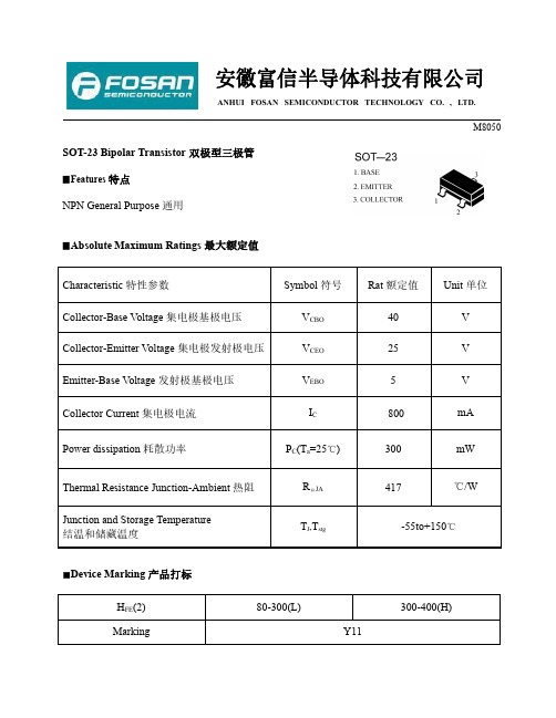
安徽富信半导体科技有限公司ANHUI FOSAN SEMICONDUCTOR TECHNOLOGY CO.,LTD.M8050 SOT-23Bipolar Transistor双极型三极管▉Features特点NPN General Purpose通用▉Absolute Maximum Ratings最大额定值Characteristic特性参数Symbol符号Rat额定值Unit单位Collector-Base Voltage集电极基极电压V CBO40V Collector-Emitter Voltage集电极发射极电压V CEO25V Emitter-Base Voltage发射极基极电压V EBO5V Collector Current集电极电流I C800mA Power dissipation耗散功率P C(T a=25℃)300mW Thermal Resistance Junction-Ambient热阻RΘJA417℃/WJunction and Storage TemperatureT J,T stg-55to+150℃结温和储藏温度■Device Marking产品打标H FE(2)80-300(L)300-400(H)Marking Y11ANHUI FOSAN SEMICONDUCTOR TECHNOLOGY CO.,LTD.M8050■ElectricalCharacteristics 电特性(T A =25℃unless otherwise noted 如无特殊说明,温度为25℃)Characteristic 特性参数Symbol 符号Min 最小值Type 典型值Max 最大值Unit 单位Collector-Base Breakdown V oltage集电极基极击穿电压(I C =100uA ,I E =0)BV CBO 40——V Collector-Emitter Breakdown Voltage 集电极发射极击穿电压(I C =1mA ,I B =0)BV CEO 25——V Emitter-Base Breakdown V oltage发射极基极击穿电压(I E =100uA ,I C =0)BV EBO 5——V Collector-Base Leakage Current集电极基极漏电流(V CB =35V ,I E =0)I CBO ——100nA Collector-Emitter Punch Throng Current 集电极发射极穿透电流(V CE =20V ,V BE =0)I CES ——100nA Emitter-Base Leakage Current发射极基极漏电流(V EB =3V ,I C =0)I EBO ——100nADC Current Gain直流电流增益(V CE =1V ,I C =5mA)H FE (1)45——DC Current Gain直流电流增益(V CE =1V ,I C =100mA)H FE (2)80—400DC Current Gain直流电流增益(V CE =1V ,I C =800mA)H FE (3)40——Collector-Emitter Saturation Voltage 集电极发射极饱和压降(I C =800mA ,I B =80mA)V CE(sat)——0.5VBase-Emitter Saturation V oltage 基极发射极饱和压降(I C =800mA ,I B =80mA)V BE(sat)—— 1.2V Transition Frequency特征频率(V CE =5V ,I C =20mA)f T —150—MH Z Output Capacitance输出电容(V CB =10V ,I E =0,f=1MH Z )C ob—6—pFANHUI FOSAN SEMICONDUCTOR TECHNOLOGY CO.,LTD.M8050■Typical Characteristic Curve典型特性曲线ANHUI FOSAN SEMICONDUCTOR TECHNOLOGY CO.,LTD.M8050■Dimension外形封装尺寸Symbol Dimensions In Millimeters Dimensions In Inches Min Max Min Max A 0.900 1.1500.0350.045A10.0000.1000.0000.004A20.900 1.0500.0350.041b 0.3000.5000.0120.020c 0.0800.1500.0030.006D 2.800 3.0000.1100.118E 1.200 1.4000.0500.055E1 2.2502.5500.0890.100e 0.950TYP0.037TYPe1 1.8002.0000.0710.079L 0.550REF0.022REFL10.3000.5000.0120.020θ0o8o 0o8o。