HY016射频设计4-静态NV生成说明教学文案
SP16系列编程器使用手册说明书

SP16系列编程器使用手册Revision B5使用编程器之前,请仔细阅读本手册,并按要求正确操作编程器,不按要求操作 将会导致编程器损坏,并得不到保修服务!深圳硕飞科技有限公司SHENZHEN SOFI TECHNOLOGY CO.,LTD .WEB: 硕飞科技目录第一章产品介绍∙∙∙∙∙∙∙∙∙∙∙∙∙∙∙∙∙∙∙∙∙∙∙∙∙∙∙∙∙∙∙∙∙∙∙∙∙∙∙∙∙∙∙∙∙∙∙∙∙∙∙∙∙∙∙∙∙∙∙∙∙∙∙∙∙∙∙∙∙∙∙∙∙∙∙∙∙∙∙∙∙∙∙∙∙∙∙∙∙∙∙∙∙∙∙∙∙∙∙∙∙∙∙∙∙∙∙∙∙∙∙∙∙∙∙∙∙∙∙∙∙3 功能特点∙∙∙∙∙∙∙∙∙∙∙∙∙∙∙∙∙∙∙∙∙∙∙∙∙∙∙∙∙∙∙∙∙∙∙∙∙∙∙∙∙∙∙∙∙∙∙∙∙∙∙∙∙∙∙∙∙∙∙∙∙∙∙∙∙∙∙∙∙∙∙∙∙∙∙∙∙∙∙∙∙∙∙∙∙∙∙∙∙∙∙∙∙∙∙∙∙∙∙∙∙∙∙∙∙∙∙∙∙∙∙∙∙∙∙∙∙∙∙∙∙3 SP16系列编程器功能对比表∙∙∙∙∙∙∙∙∙∙∙∙∙∙∙∙∙∙∙∙∙∙∙∙∙∙∙∙∙∙∙∙∙∙∙∙∙∙∙∙∙∙∙∙∙∙∙∙∙∙∙∙∙∙∙∙∙∙∙∙∙∙∙∙∙∙∙∙∙∙∙∙∙∙∙∙∙∙∙∙∙∙∙∙∙∙∙∙∙∙∙∙∙ 4 第二章编程器硬件∙∙∙∙∙∙∙∙∙∙∙∙∙∙∙∙∙∙∙∙∙∙∙∙∙∙∙∙∙∙∙∙∙∙∙∙∙∙∙∙∙∙∙∙∙∙∙∙∙∙∙∙∙∙∙∙∙∙∙∙∙∙∙∙∙∙∙∙∙∙∙∙∙∙∙∙∙∙∙∙∙∙∙∙∙∙∙∙∙∙∙∙∙∙∙∙∙∙∙∙∙∙∙∙∙∙∙∙∙∙∙∙∙∙∙∙∙∙5 第三章快速使用∙∙∙∙∙∙∙∙∙∙∙∙∙∙∙∙∙∙∙∙∙∙∙∙∙∙∙∙∙∙∙∙∙∙∙∙∙∙∙∙∙∙∙∙∙∙∙∙∙∙∙∙∙∙∙∙∙∙∙∙∙∙∙∙∙∙∙∙∙∙∙∙∙∙∙∙∙∙∙∙∙∙∙∙∙∙∙∙∙∙∙∙∙∙∙∙∙∙∙∙∙∙∙∙∙∙∙∙∙∙∙∙∙∙∙∙∙∙∙∙∙6 联机模式烧录步骤∙∙∙∙∙∙∙∙∙∙∙∙∙∙∙∙∙∙∙∙∙∙∙∙∙∙∙∙∙∙∙∙∙∙∙∙∙∙∙∙∙∙∙∙∙∙∙∙∙∙∙∙∙∙∙∙∙∙∙∙∙∙∙∙∙∙∙∙∙∙∙∙∙∙∙∙∙∙∙∙∙∙∙∙∙∙∙∙∙∙∙∙∙∙∙∙∙∙∙∙∙∙∙∙∙∙∙ 6 联机烧录模式指示灯状态说明∙∙∙∙∙∙∙∙∙∙∙∙∙∙∙∙∙∙∙∙∙∙∙.∙∙∙∙∙∙∙∙∙∙∙∙∙∙∙∙∙∙∙∙∙∙∙∙∙∙∙∙∙∙∙∙∙∙∙∙∙∙∙∙∙∙∙∙∙∙∙∙∙∙∙∙∙∙∙∙∙∙∙∙∙∙∙∙∙∙∙8 第四章脱机烧录∙∙∙∙∙∙∙∙∙∙∙∙∙∙∙∙∙∙∙∙∙∙∙∙∙∙∙∙∙∙∙∙∙∙∙∙∙∙∙∙∙∙∙∙∙∙∙∙∙∙∙∙∙∙∙∙∙∙∙∙∙∙∙∙∙∙∙∙∙∙∙∙∙∙∙∙∙∙∙∙∙∙∙∙∙∙∙∙∙∙∙∙∙∙∙∙∙∙∙∙∙∙∙∙∙∙∙∙∙∙∙∙∙∙∙∙∙∙∙∙∙9 下载脱机数据∙∙∙∙∙∙∙∙∙∙∙∙∙∙∙∙∙∙∙∙∙∙∙∙∙∙∙∙∙∙∙∙∙∙∙∙∙∙∙∙∙∙∙∙∙∙∙∙∙∙∙∙∙∙∙∙∙∙∙∙∙∙∙∙∙∙∙∙∙∙∙∙∙∙∙∙∙∙∙∙∙∙∙∙∙∙∙∙∙∙∙∙∙∙∙∙∙∙∙∙∙∙∙∙∙∙∙∙∙∙∙∙∙∙9 脱机运行–手动方式∙∙∙∙∙∙∙∙∙∙∙∙∙∙∙∙∙∙∙∙∙∙∙∙∙∙∙∙∙∙∙∙∙∙∙∙∙∙∙∙∙∙∙∙∙∙∙∙∙∙∙∙∙∙∙∙∙∙∙∙∙∙∙∙∙∙∙∙∙∙∙∙∙∙∙∙∙∙∙∙∙∙∙∙∙∙∙∙∙∙∙∙∙∙∙∙∙∙∙∙∙∙10 脱机运行–自动控制方式∙∙∙∙∙∙∙∙∙∙∙∙∙∙∙∙∙∙∙∙∙∙∙∙∙∙∙∙∙∙∙∙∙∙∙∙∙∙∙∙∙∙∙∙∙∙∙∙∙∙∙∙∙∙∙∙∙∙∙∙∙∙∙∙∙∙∙∙∙∙∙∙∙∙∙∙∙∙∙∙∙∙∙∙∙∙∙∙∙∙∙∙∙∙∙∙10 ATE接口定义∙∙∙∙∙∙∙∙∙∙∙∙∙∙∙∙∙∙∙∙∙∙∙∙∙∙∙∙∙∙∙∙∙∙∙∙∙∙∙∙∙∙∙∙∙∙∙∙∙∙∙∙∙∙∙∙∙∙∙∙∙∙∙∙∙∙∙∙∙∙∙∙∙∙∙∙∙∙∙∙∙∙∙∙∙∙∙∙∙∙∙∙∙∙∙∙∙∙∙∙∙∙∙∙∙∙∙∙∙∙∙∙10 脱机工作模式状态指示灯∙∙∙∙∙∙∙∙∙∙∙∙∙∙∙∙∙∙∙∙∙∙∙∙∙∙∙∙∙∙∙∙∙∙∙∙∙∙∙∙∙∙∙∙∙∙∙∙∙∙∙∙∙∙∙∙∙∙∙∙∙∙∙∙∙∙∙∙∙∙∙∙∙∙∙∙∙∙∙∙∙∙∙∙∙∙∙∙∙∙∙∙∙∙∙∙∙∙ 11 脱机数据查看∙∙∙∙∙∙∙∙∙∙∙∙∙∙∙∙∙∙∙∙∙∙∙∙∙∙∙∙∙∙∙∙∙∙∙∙∙∙∙∙∙∙∙∙∙∙∙∙∙∙∙∙∙∙∙∙∙∙∙∙∙∙∙∙∙∙∙∙∙∙∙∙∙∙∙∙∙∙∙∙∙∙∙∙∙∙∙∙∙∙∙∙∙∙∙∙∙∙∙∙∙∙∙∙∙∙∙∙∙∙∙∙∙∙∙11 第五章ISP 模式烧录∙∙∙∙∙∙∙∙∙∙∙∙∙∙∙∙∙∙∙∙∙∙∙∙∙∙∙∙∙∙∙∙∙∙∙∙∙∙∙∙∙∙∙∙∙∙∙∙∙∙∙∙∙∙∙∙∙∙∙∙∙∙∙∙∙∙∙∙∙∙∙∙∙∙∙∙∙∙∙∙∙∙∙∙∙∙∙∙∙∙∙∙∙∙∙∙∙∙∙∙∙∙∙∙∙∙∙∙∙∙∙∙∙12 ISP接口∙∙∙∙∙∙∙∙∙∙∙∙∙∙∙∙∙∙∙∙∙∙∙∙∙∙∙∙∙∙∙∙∙∙∙∙∙∙∙∙∙∙∙∙∙∙∙∙∙∙∙∙∙∙∙∙∙∙∙∙∙∙∙∙∙∙∙∙∙∙∙∙∙∙∙∙∙∙∙∙∙∙∙∙∙∙∙∙∙∙∙∙∙∙∙∙∙∙∙∙∙∙∙∙∙∙∙∙∙∙∙∙∙∙∙∙∙∙∙∙12 ISP连接线∙∙∙∙∙∙∙∙∙∙∙∙∙∙∙∙∙∙∙∙∙∙∙∙∙∙∙∙∙∙∙∙∙∙∙∙∙∙∙∙∙∙∙∙∙∙∙∙∙∙∙∙∙∙∙∙∙∙∙∙∙∙∙∙∙∙∙∙∙∙∙∙∙∙∙∙∙∙∙∙∙∙∙∙∙∙∙∙∙∙∙∙∙∙∙∙∙∙∙∙∙∙∙∙∙∙∙∙∙∙∙∙∙∙∙∙∙12 目标芯片连接∙∙∙∙∙∙∙∙∙∙∙∙∙∙∙∙∙∙∙∙∙∙∙∙∙∙∙∙∙∙∙∙∙∙∙∙∙∙∙∙∙∙∙∙∙∙∙∙∙∙∙∙∙∙∙∙∙∙∙∙∙∙∙∙∙∙∙∙∙∙∙∙∙∙∙∙∙∙∙∙∙∙∙∙∙∙∙∙∙∙∙∙∙∙∙∙∙∙∙∙∙∙∙∙∙∙∙∙∙∙∙∙∙13 ISP供电模式∙∙∙∙∙∙∙∙∙∙∙∙∙∙∙∙∙∙∙∙∙∙∙∙∙∙∙∙∙∙∙∙∙∙∙∙∙∙∙∙∙∙∙∙∙∙∙∙∙∙∙∙∙∙∙∙∙∙∙∙∙∙∙∙∙∙∙∙∙∙∙∙∙∙∙∙∙∙∙∙∙∙∙∙∙∙∙∙∙∙∙∙∙∙∙∙∙∙∙∙∙∙∙∙∙∙∙∙∙∙∙∙∙14 第六章FlyPRO MCP多机控制软件∙∙∙∙∙∙∙∙∙∙∙∙∙∙∙∙∙∙∙∙∙∙∙∙∙∙∙∙∙∙∙∙∙∙∙∙∙∙∙∙∙∙∙∙∙∙∙∙∙∙∙∙∙∙∙∙∙∙∙∙∙∙∙∙∙∙∙∙∙∙∙∙∙∙∙∙∙∙∙∙∙∙∙∙∙∙∙∙∙∙∙∙∙∙15 功能介绍∙∙∙∙∙∙∙∙∙∙∙∙∙∙∙∙∙∙∙∙∙∙∙∙∙∙∙∙∙∙∙∙∙∙∙∙∙∙∙∙∙∙∙∙∙∙∙∙∙∙∙∙∙∙∙∙∙∙∙∙∙∙∙∙∙∙∙∙∙∙∙∙∙∙∙∙∙∙∙∙∙∙∙∙∙∙∙∙∙∙∙∙∙∙∙∙∙∙∙∙∙∙∙∙∙∙∙∙∙∙∙∙∙∙∙∙∙∙∙∙15 使用方法∙∙∙∙∙∙∙∙∙∙∙∙∙∙∙∙∙∙∙∙∙∙∙∙∙∙∙∙∙∙∙∙∙∙∙∙∙∙∙∙∙∙∙∙∙∙∙∙∙∙∙∙∙∙∙∙∙∙∙∙∙∙∙∙∙∙∙∙∙∙∙∙∙∙∙∙∙∙∙∙∙∙∙∙∙∙∙∙∙∙∙∙∙∙∙∙∙∙∙∙∙∙∙∙∙∙∙∙∙∙∙∙∙∙∙∙∙∙∙∙∙15 附录一常见问题∙∙∙∙∙∙∙∙∙∙∙∙∙∙∙∙∙∙∙∙∙∙∙∙∙∙∙∙∙∙∙∙∙∙∙∙∙∙∙∙∙∙∙∙∙∙∙∙∙∙∙∙∙∙∙∙∙∙∙∙∙∙∙∙∙∙∙∙∙∙∙∙∙∙∙∙∙∙∙∙∙∙∙∙∙∙∙∙∙∙∙∙∙∙∙∙∙∙∙∙∙∙∙∙∙∙∙∙∙∙∙∙∙∙∙∙∙∙∙∙∙19 附录二免责声明∙∙∙∙∙∙∙∙∙∙∙∙∙∙∙∙∙∙∙∙∙∙∙∙∙∙∙∙∙∙∙∙∙∙∙∙∙∙∙∙∙∙∙∙∙∙∙∙∙∙∙∙∙∙∙∙∙∙∙∙∙∙∙∙∙∙∙∙∙∙∙∙∙∙∙∙∙∙∙∙∙∙∙∙∙∙∙∙∙∙∙∙∙∙∙∙∙∙∙∙∙∙∙∙∙∙∙∙∙∙∙∙∙∙∙∙∙∙∙∙∙21 附录三文件修订记录信息∙∙∙∙∙∙∙∙∙∙∙∙∙∙∙∙∙∙∙∙∙∙∙∙∙∙∙∙∙∙∙∙∙∙∙∙∙∙∙∙∙∙∙∙∙∙∙∙∙∙∙∙∙∙∙∙∙∙∙∙∙∙∙∙∙∙∙∙∙∙∙∙∙∙∙∙∙∙∙∙∙∙∙∙∙∙∙∙∙∙∙∙∙∙∙∙∙∙∙∙∙∙∙∙∙∙∙∙22第一章产品介绍功能特点⚫专门针对串行EEPROM / SPI FLASH芯片进行设计,相比于通用编程器速度更快,稳定性更高;⚫USB供电及通讯,无需外接电源。
16m晶振写延时

16MHz晶振写延时可以通过公式进行计算,公式为:T = 1.15/(f x 2^N),其中T为晶振频率对应的周期,f为晶振频率,N为相位常数。
根据这个公式,可以得出需要的延时时间。
一般来说,可以使用Keil或IAR等开发工具中的定时器进行延时。
在C语言中,可以使用delay()函数实现延时操作。
在编写代码时,需要根据实际情况选择合适的延时时间,并注意避免程序中出现死循环等问题。
具体步骤如下:
1. 根据晶振频率和相位常数,使用公式计算出需要的延时时间。
2. 在Keil或IAR等开发工具中,选择合适的定时器进行延时操作。
3. 在主程序中调用delay()函数实现延时操作。
4. 根据实际需要,对程序进行调试和优化,确保程序能够正常运行。
注意事项:
1. 在编写代码时,需要注意避免程序中出现死循环等问题,以免影响程序的正常运行。
2. 在使用晶振时,需要注意晶振的安装方式和连接方式是否正确,以免影响晶振的性能和稳定性。
3. 在编写代码时,需要考虑到晶振的频率误差等因素,并采取相应的措施进行处理。
总之,通过以上步骤和注意事项,可以有效地实现16MHz晶振写延时操作。
需要注意的是,在实际应用中,需要根据具体情况进行调整和优化,以确保程序的正确性和稳定性。
DDR4设计概述以及分析仿真案例演示教学

D D R4设计概述以及分析仿真案例DRAM (动态随机访问存储器)对设计人员特别具有吸引力,因为它提供了广泛的性能,用于各种计算机和嵌入式系统的存储系统设计中。
本文概括阐述了DRAM 的概念,及介绍了SDRAM、DDR SDRAM、DDR2 SDRAM、DDR3 SDRAM、DDR4 SDRAM、DDR5 SDRAM、LPDDR、GDDR。
DRAMDRAM较其它内存类型的一个优势是它能够以IC(集成电路)上每个内存单元更少的电路实现。
DRAM 的内存单元基于电容器上贮存的电荷。
典型的DRAM 单元使用一个电容器及一个或三个FET(场效应晶体管)制成。
典型的SRAM (静态随机访问内存)内存单元采取六个FET 器件,降低了相同尺寸时每个IC 的内存单元数量。
与DRAM 相比,SRAM 使用起来更简便,接口更容易,数据访问时间更快。
DRAM核心结构由多个内存单元组成,这些内存单元分成由行和列组成的两维阵列(参见图1)。
访问内存单元需要两步。
先寻找某个行的地址,然后在选定行中寻找特定列的地址。
换句话说,先在DRAM IC 内部读取整个行,然后列地址选择DRAM IC I/O(输入/ 输出)针脚要读取或要写入该行的哪一列。
DRAM读取具有破坏性,也就是说,在读操作中会破坏内存单元行中的数据。
因此,必需在该行上的读或写操作结束时,把行数据写回到同一行中。
这一操作称为预充电,是行上的最后一项操作。
必须完成这一操作之后,才能访问新的行,这一操作称为关闭打开的行。
对计算机内存访问进行分析后表明,内存访问中最常用的类型是读取顺序的内存地址。
这是合理的,因为读取计算机指令一般要比数据读取或写入更加常用。
此外,大多数指令读取在内存中顺序进行,直到发生到指令分支或跳到子例程。
图1. DRAMs 内存单元分成由行和列组成的两维阵列DRAM的一个行称为内存页面,一旦打开行,您可以访问该行中多个顺序的或不同的列地址。
这提高了内存访问速度,降低了内存时延,因为在访问同一个内存页面中的内存单元时,其不必把行地址重新发送给DRAM.结果,行地址是计算机的高阶地址位,列地址是低阶地址位。
第6章(486)
第6章 VHDL程序设计实验 图6.3 工程属性参数
第6章 VHDL程序设计实验
2.逻辑门的RTL描述 编写MY_AND2实体的VHDL代码。 (1) 选择菜单栏中的 Project→New Source。 (2) 在 Select Source Type 窗口中,选择左侧VHDL Module,在右侧 File Name栏中填入文件名MY_AND2,单 击Next按钮后弹出Define Module窗口,如图6.4所示。
entity MY_AND2 is port ( A: in STD_LOGIC; B: in STD_LOGIC; C: out STD_LOGIC);
end MY_AND2;
architecture BEHAVIORAL of MY_AND2 is begin
C <= A and B; end BEHAVIORAL;
(2) 将AND_OR.VHD的输入定义为一个总线,即STD_ LOGIC_VECTOR类型。
(3) 在AND_OR模块中,必须声明和例化被调用的下层 模块MY_AND2和MY_OR2。
(4) 在AND_OR模块中,必须显式地定义用于下层模块 互联的连线信号。
(5) MY_OR2和AND_OR模块的代码可以参照本实验后 面给出的代码实例。
本实验中会用到3个文件,文件对应的代码分别下:
MY_AND2.VH D
library IEEE; use IEEE.STD_LOGIC_1164.all; use IEEE.STD_LOGIC_ARITH. all; use IEEE.STD_LOGIC_UNSIGNED. all;
第6章 VHDL程序设计实验
end MY_AND2;
第6章 VHDL程序设计实验
SP16系列编程器用户手册说明书

SP16 SERIES PROGRAMMERUSER MANUALRevision B5Before using the programmer, please read this manual carefully and operate the programmer correctly as required. Failure to follow the instructions will result in damage to the programmer and no warranty service!深圳硕飞科技有限公司SHENZHEN SOFI TECHNOLOGY CO.,LTD .WEB: 硕飞科技ContentsChapter1. Introduction into Products ∙∙∙∙∙∙∙∙∙∙∙∙∙∙∙∙∙∙∙∙∙∙∙∙∙∙∙∙∙∙∙∙∙∙∙∙∙∙∙∙∙∙∙∙∙∙∙∙∙∙∙∙∙∙∙∙∙∙∙∙∙∙∙∙∙∙∙∙∙∙∙∙∙∙∙∙∙∙∙∙∙∙∙∙∙∙∙∙∙∙∙∙ 3 Performance and Characters∙∙∙∙∙∙∙∙∙∙∙∙∙∙∙∙∙∙∙∙∙∙∙∙∙∙∙∙∙∙∙∙∙∙∙∙∙∙∙∙∙∙∙∙∙∙∙∙∙∙∙∙∙∙∙∙∙∙∙∙∙∙∙∙∙∙∙∙∙∙∙∙∙∙∙∙∙∙∙∙∙∙∙∙∙∙∙∙∙∙∙∙ 3Correlation Table of SP16 Performance∙∙∙∙∙∙∙∙∙∙∙∙∙∙∙∙∙∙∙∙∙∙∙∙∙∙∙∙∙∙∙∙∙∙∙∙∙∙∙∙∙∙∙∙∙∙∙∙∙∙∙∙∙∙∙∙∙∙∙∙∙∙∙∙∙∙∙∙∙∙∙∙∙∙∙∙∙∙ 4 Chapter 2. Programmer Hardware∙∙∙∙∙∙∙∙∙∙∙∙∙∙∙∙∙∙∙∙∙∙∙∙∙∙∙∙∙∙∙∙∙∙∙∙∙∙∙∙∙∙∙∙∙∙∙∙∙∙∙∙∙∙∙∙∙∙∙∙∙∙∙∙∙∙∙∙∙∙∙∙∙∙∙∙∙∙∙∙∙∙∙∙∙∙∙∙∙∙∙∙∙∙∙∙∙∙ 5 Chapter 3. Quick start∙∙∙∙∙∙∙∙∙∙∙∙∙∙∙∙∙∙∙∙∙∙∙∙∙∙∙∙∙∙∙∙∙∙∙∙∙∙∙∙∙∙∙∙∙∙∙∙∙∙∙∙∙∙∙∙∙∙∙∙∙∙∙∙∙∙∙∙∙∙∙∙∙∙∙∙∙∙∙∙∙∙∙∙∙∙∙∙∙∙∙∙∙∙∙∙∙∙∙∙∙∙∙∙∙∙∙∙∙∙∙∙∙∙∙∙ 6 Programming steps for on-line mode∙∙∙∙∙∙∙∙∙∙∙∙∙∙∙∙∙∙∙∙∙∙∙∙∙∙∙∙∙∙∙∙∙∙∙∙∙∙∙∙∙∙∙∙∙∙∙∙∙∙∙∙∙∙∙∙∙∙∙∙∙∙∙∙∙∙∙∙∙∙∙∙∙∙∙∙∙∙∙∙∙∙ 6LED status for On-line programming mode∙∙∙∙∙∙∙∙∙∙∙∙∙∙∙∙∙∙∙∙∙∙∙∙∙∙∙∙∙∙∙∙∙∙∙∙∙∙∙∙∙∙∙∙∙∙∙∙∙∙∙∙∙∙∙∙∙∙∙∙∙∙∙∙∙∙∙∙∙∙∙∙∙∙ 8 Chapter 4. Off-line programming∙∙∙∙∙∙∙∙∙∙∙∙∙∙∙∙∙∙∙∙∙∙∙∙∙∙∙∙∙∙∙∙∙∙∙∙∙∙∙∙∙∙∙∙∙∙∙∙∙∙∙∙∙∙∙∙∙∙∙∙∙∙∙∙∙∙∙∙∙∙∙∙∙∙∙∙∙∙∙∙∙∙∙∙∙∙∙∙∙∙∙∙∙∙∙∙∙∙ 10 Download Off-line Data∙∙∙∙∙∙∙∙∙∙∙∙∙∙∙∙∙∙∙∙∙∙∙∙∙∙∙∙∙∙∙∙∙∙∙∙∙∙∙∙∙∙∙∙∙∙∙∙∙∙∙∙∙∙∙∙∙∙∙∙∙∙∙∙∙∙∙∙∙∙∙∙∙∙∙∙∙∙∙∙∙∙∙∙∙∙∙∙∙∙∙∙∙∙∙∙∙∙ 10Off-line Operation - Manual Mode∙∙∙∙∙∙∙∙∙∙∙∙∙∙∙∙∙∙∙∙∙∙∙∙∙∙∙∙∙∙∙∙∙∙∙∙∙∙∙∙∙∙∙∙∙∙∙∙∙∙∙∙∙∙∙∙∙∙∙∙∙∙∙∙∙∙∙∙∙∙∙∙∙∙∙∙∙∙∙∙∙∙∙∙ 12Off-line Operation - Automatic Control Mode∙∙∙∙∙∙∙∙∙∙∙∙∙∙∙∙∙∙∙∙∙∙∙∙∙∙∙∙∙∙∙∙∙∙∙∙∙∙∙∙∙∙∙∙∙∙∙∙∙∙∙∙∙∙∙∙∙∙∙∙∙∙∙∙∙∙∙∙∙ 12ATE interface definitions∙∙∙∙∙∙∙∙∙∙∙∙∙∙∙∙∙∙∙∙∙∙∙∙∙∙∙∙∙∙∙∙∙∙∙∙∙∙∙∙∙∙∙∙∙∙∙∙∙∙∙∙∙∙∙∙∙∙∙∙∙∙∙∙∙∙∙∙∙∙∙∙∙∙∙∙∙∙∙∙∙∙∙∙∙∙∙∙∙∙∙∙∙∙∙∙∙ 12LED status for off-line programming mode ∙∙∙∙∙∙∙∙∙∙∙∙∙∙∙∙∙∙∙∙∙∙∙∙∙∙∙∙∙∙∙∙∙∙∙∙∙∙∙∙∙∙∙∙∙∙∙∙∙∙∙∙∙∙∙∙∙∙∙∙∙∙∙∙∙∙∙∙∙∙∙ 12View Off-line Data ∙∙∙∙∙∙∙∙∙∙∙∙∙∙∙∙∙∙∙∙∙∙∙∙∙∙∙∙∙∙∙∙∙∙∙∙∙∙∙∙∙∙∙∙∙∙∙∙∙∙∙∙∙∙∙∙∙∙∙∙∙∙∙∙∙∙∙∙∙∙∙∙∙∙∙∙∙∙∙∙∙∙∙∙∙∙∙∙∙∙∙∙∙∙∙∙∙∙∙∙∙∙∙∙∙ 13 Chapter 5.ISP Programming∙∙∙∙∙∙∙∙∙∙∙∙∙∙∙∙∙∙∙∙∙∙∙∙∙∙∙∙∙∙∙∙∙∙∙∙∙∙∙∙∙∙∙∙∙∙∙∙∙∙∙∙∙∙∙∙∙∙∙∙∙∙∙∙∙∙∙∙∙∙∙∙∙∙∙∙∙∙∙∙∙∙∙∙∙∙∙∙∙∙∙∙∙∙∙∙∙∙∙∙∙∙∙∙ 14 Use ISP programming mode∙∙∙∙∙∙∙∙∙∙∙∙∙∙∙∙∙∙∙∙∙∙∙∙∙∙∙∙∙∙∙∙∙∙∙∙∙∙∙∙∙∙∙∙∙∙∙∙∙∙∙∙∙∙∙∙∙∙∙∙∙∙∙∙∙∙∙∙∙∙∙∙∙∙∙∙∙∙∙∙∙∙∙∙∙∙∙∙∙∙∙ 14ISP Interface∙∙∙∙∙∙∙∙∙∙∙∙∙∙∙∙∙∙∙∙∙∙∙∙∙∙∙∙∙∙∙∙∙∙∙∙∙∙∙∙∙∙∙∙∙∙∙∙∙∙∙∙∙∙∙∙∙∙∙∙∙∙∙∙∙∙∙∙∙∙∙∙∙∙∙∙∙∙∙∙∙∙∙∙∙∙∙∙∙∙∙∙∙∙∙∙∙∙∙∙∙∙∙∙∙∙∙∙∙∙∙∙∙ 14ISP cable∙∙∙∙∙∙∙∙∙∙∙∙∙∙∙∙∙∙∙∙∙∙∙∙∙∙∙∙∙∙∙∙∙∙∙∙∙∙∙∙∙∙∙∙∙∙∙∙∙∙∙∙∙∙∙∙∙∙∙∙∙∙∙∙∙∙∙∙∙∙∙∙∙∙∙∙∙∙∙∙∙∙∙∙∙∙∙∙∙∙∙∙∙∙∙∙∙∙∙∙∙∙∙∙∙∙∙∙∙∙∙∙∙∙∙∙∙∙ 14Target devices connections∙∙∙∙∙∙∙∙∙∙∙∙∙∙∙∙∙∙∙∙∙∙∙∙∙∙∙∙∙∙∙∙∙∙∙∙∙∙∙∙∙∙∙∙∙∙∙∙∙∙∙∙∙∙∙∙∙∙∙∙∙∙∙∙∙∙∙∙∙∙∙∙∙∙∙∙∙∙∙∙∙∙∙∙∙∙∙∙∙∙∙∙∙ 15ISP Power supply mode∙∙∙∙∙∙∙∙∙∙∙∙∙∙∙∙∙∙∙∙∙∙∙∙∙∙∙∙∙∙∙∙∙∙∙∙∙∙∙∙∙∙∙∙∙∙∙∙∙∙∙∙∙∙∙∙∙∙∙∙∙∙∙∙∙∙∙∙∙∙∙∙∙∙∙∙∙∙∙∙∙∙∙∙∙∙∙∙∙∙∙∙∙∙∙∙∙∙ 16 Chapter 6. FlyPRO MCP multi-machine control software∙∙∙∙∙∙∙∙∙∙∙∙∙∙∙∙∙∙∙∙∙∙∙∙∙∙∙∙∙∙∙∙∙∙∙∙∙∙∙∙∙∙∙∙∙∙∙∙∙∙∙∙∙∙∙∙∙∙∙∙∙∙∙∙ 17 Function Introduction∙∙∙∙∙∙∙∙∙∙∙∙∙∙∙∙∙∙∙∙∙∙∙∙∙∙∙∙∙∙∙∙∙∙∙∙∙∙∙∙∙∙∙∙∙∙∙∙∙∙∙∙∙∙∙∙∙∙∙∙∙∙∙∙∙∙∙∙∙∙∙∙∙∙∙∙∙∙∙∙∙∙∙∙∙∙∙∙∙∙∙∙∙∙∙∙∙∙∙∙∙∙ 17Usage Instruction∙∙∙∙∙∙∙∙∙∙∙∙∙∙∙∙∙∙∙∙∙∙∙∙∙∙∙∙∙∙∙∙∙∙∙∙∙∙∙∙∙∙∙∙∙∙∙∙∙∙∙∙∙∙∙∙∙∙∙∙∙∙∙∙∙∙∙∙∙∙∙∙∙∙∙∙∙∙∙∙∙∙∙∙∙∙∙∙∙∙∙∙∙∙∙∙∙∙∙∙∙∙∙∙∙∙∙ 17FlyPRO_MCP function limitations∙∙∙∙∙∙∙∙∙∙∙∙∙∙∙∙∙∙∙∙∙∙∙∙∙∙∙∙∙∙∙∙∙∙∙∙∙∙∙∙∙∙∙∙∙∙∙∙∙∙∙∙∙∙∙∙∙∙∙∙∙∙∙∙∙∙∙∙∙∙∙∙∙∙∙∙∙∙∙∙∙∙∙∙∙ 19About USB hub∙∙∙∙∙∙∙∙∙∙∙∙∙∙∙∙∙∙∙∙∙∙∙∙∙∙∙∙∙∙∙∙∙∙∙∙∙∙∙∙∙∙∙∙∙∙∙∙∙∙∙∙∙∙∙∙∙∙∙∙∙∙∙∙∙∙∙∙∙∙∙∙∙∙∙∙∙∙∙∙∙∙∙∙∙∙∙∙∙∙∙∙∙∙∙∙∙∙∙∙∙∙∙∙∙∙∙∙∙∙ 19 Appendix I FAQ∙∙∙∙∙∙∙∙∙∙∙∙∙∙∙∙∙∙∙∙∙∙∙∙∙∙∙∙∙∙∙∙∙∙∙∙∙∙∙∙∙∙∙∙∙∙∙∙∙∙∙∙∙∙∙∙∙∙∙∙∙∙∙∙∙∙∙∙∙∙∙∙∙∙∙∙∙∙∙∙∙∙∙∙∙∙∙∙∙∙∙∙∙∙∙∙∙∙∙∙∙∙∙∙∙∙∙∙∙∙∙∙∙∙∙∙∙∙∙∙∙∙∙∙∙20 Appendix II Disclaimer ∙∙∙∙∙∙∙∙∙∙∙∙∙∙∙∙∙∙∙∙∙∙∙∙∙∙∙∙∙∙∙∙∙∙∙∙∙∙∙∙∙∙∙∙∙∙∙∙∙∙∙∙∙∙∙∙∙∙∙∙∙∙∙∙∙∙∙∙∙∙∙∙∙∙∙∙∙∙∙∙∙∙∙∙∙∙∙∙∙∙∙∙∙∙∙∙∙∙∙∙∙∙∙∙∙∙∙∙∙∙∙∙∙ 22 Appendix III Revision history ∙∙∙∙∙∙∙∙∙∙∙∙∙∙∙∙∙∙∙∙∙∙∙∙∙∙∙∙∙∙∙∙∙∙∙∙∙∙∙∙∙∙∙∙∙∙∙∙∙∙∙∙∙∙∙∙∙∙∙∙∙∙∙∙∙∙∙∙∙∙∙∙∙∙∙∙∙∙∙∙∙∙∙∙∙∙∙∙∙∙∙∙∙∙∙∙∙∙∙∙∙∙∙ 23Chapter 1. Introduction into ProductsPerformance and characters⚫Designed specifically for serial EEPROM / SPI FLASH device, faster and more stable than general-purpose programmer⚫USB power supply and communication, no external power supply required. Small size (size: 103x71x23mm), easy to carry⚫Supports a full range of 93/24/25/BR90 memories, supports software upgrades to increase support for new devices⚫Supports detection of 25 series SPI FLASH device models;⚫Supports pin contact detection to improve the reliability of programing;⚫Supports ISP program. On-board patch devices can be directly connected to be programmed⚫Standard 40Pin ZIF socket, applicable to wide/narrow devices and general adapters⚫Overcurrent protection function to effectively prevent misplaced or destroyed device’s effects on the programmer;⚫Programmer has a built-in 32-bit high-speed processor that provides high-speed programming and precise timing;⚫Supports off-line programming without connecting computers. Has a large data memory built-in that can supports up to 512Mbit device to program off-line (Note 1);⚫Mass production programming mode, automatic detection of device placement and start programming operation;⚫ATE interface function that supports automatic programming machine to control (Note 2);⚫Supports one computer to connect multiple programmers programming at the same time, one computer can connect up to 8 programmers⚫The buzzer present voice prompt for success or failure⚫Programmable voltage design, adjustable from 1.7V to 5.0V, supporting 1.8V/2.5V/3V/3.3V/5V devices; ⚫Provide device self-test function;⚫Support WinXP (SP2), VISTA, Win7/Win8/Win10 (32bit/64bit)Note 1: Off-line operation is limited to SP16-F, SP16-FX mode; off-line program does not support ISP mode Note 2: SP16-FX mode onlyCorrelation table of SP16 performanceModel SP16-FX SP16-F SP16-B maximum capacity of Supporteddevices512MbSupported device voltage programmable voltage adjustable from 1.7V to 5.0V , supports1.8V/2.5V/3V/3.3V/5V...Off-line programming (Note 1)Y Y N Built-in memory for off-line data 512Mb -On-line mass production (Note 1)Y (automatic detection device placement/removal) Multi connection (Note 2)YAuto serial number Y(On-line program mode only)Buzzer prompt Y (off-line mode only) N Overcurrent/short circuit protection YZIF Socket ARIESISP programming Support 24/93/25 series (clock adjustable) OTP area read and write (Note 3)supportDevice configuration (Note 3)supportAutomatic programing MachineSupport (ATE)Y N Nprograming speed (Note 4)GD25Q16(SOP8) Off-line P+V=6S; on-line P+V=7S W25Q128FV(SOP8) Off-line P+V=47S; on-line P+V=52S MX25L12845E(SOP16) Off-line P+V=62S; on-line P+V=68Soff-line data download speeds 41S@128Mb -Support the number of devices(Note 5)10284 10284Note 1: Off-line programming means the model can program without computer, suitable for mass production.On-line mass production refers to connecting to a computer for batch programming.Note 2: One computer can maximum connect eight SP16 series programmers (need to work together with FlyPRO_MCP software, search Chapter 6 for specific usage);Note 3: Depending on the software function, not all the devices are supported;Note 4: The programming speed is tested by the complete device random number, “P” is programming, V “is”verification;Note 5: Based on FlyPRO software version V4.48 (2019-05-29). The devices will increase with software upgrades. The number in the table is for reference only. Please download the latest supported software from Sofi official website download center.Chapter 2. Programmer hardwareProgrammerAccessoriesUSB Cable ISP Cable 5V/1A Power adapter⚫ The appearance of different models and batches may vary, please refer to the actualproduct;⚫ The power adapter is used to power the programmer during offline programming, andonly SP16-F/SP16-FX which supports offline programming has equipped ;⚫ The programmer is equipped with a device adapter (IC socket) as standard, pleasechoose according to your needs.USB InterfaceZIF SocketPWR(Power) STA(State) ISP/ATE InterfaceChapter 3. Quick startProgramming steps for on-line mode1. Install programmer control software: FlyPRO (Includes USB driver, single control software FlyPRO,multi-control software FlyPRO), software download website: 2. Connect programmer to USB port of computer with a USB cable.3. Run the single control software FlyPRO ,the programmer hardware will be automatically connected afterthe software starts. After the connection is successful, the software status bar will display theprogrammer mode and product serial number, and then you can program devices.The following takes a device W25Q32BV packaged of SOIC8 (208mil) as an example to introduce the steps of programming devices:4. Click the toolbar button,or menu [Device] - [Select Device], open the "Select Device" dialog box, select the device model to be programmed and the corresponding package"W25Q32BV[SOIC8]". You can quickly find the device by entering the device model keyword through the search box.Connect to computer USB portNOTE:The “W25Q32BV” in the device listdoes not have a “[ ]” suffix,indicating that the model is an DIPdevice;"[SOIC8]", "[SOIC16]", "[WSON88x6]", "[WSON8 6x5]", etc. indicatethe package type of device;“[ISP]” means to use ISP mode toprogram, please refer to “Chapter5. ISP progr amming”.5. Load programming fileClick toolbar button,or menu [File] - [Load File] to load the data file of program.6. Set operation optionsClick the toolbar button,or menu [Operation] - [Operational Options] to deviceprogramming settings. In most cases, you can use the default settings. For details on the operation options, please refer to the helper topic of the programmer software.7. Place device to ZIF SocketThe DIP packaged device can be directly inserted, and the non-straight-inserted device needs to be matched with IC socket. In this example, an SOP8 wide-body programing seat is used. First, lift ZIF Socket’s handle, insert the bottom side of IC socket into the bottom of ZIF Socket, press the handle, and then put the device into IC socket. Pay attention to the direction of the first leg of device.Pin1 Pin1Physical map Device pin position diagram For other device s’ placement (including IC socket information), please open the device information in the FlyPRO software for viewing. Most of 8-pin devices are inserted into ZIF Socket according to thecorresponding relationship on the right. A very small number of devices are placed in a special way.Please pay attention to the prompts that the software pops up.Note: ZIF Socket is only used to place the device to be programmed (including IC socket). It is forbidden to programming devices which have already been welded on circuit board, through wires from ZIF socket. The peripheral circuit on the board will cause the operation to fail. Serious conditions can cause permanent damage to the programmer hardware. The manufacturer is not responsible for anyconsequences that may result from this incorrect operation. The EMI method is recommended for the device that has been soldered. Please refer to "Chapter 5. ISP Programming".8. Perform programmingThere are three modes for programming, including manual mode, automatic mode, and automatic mass production mode. Choose one of the modes to operate according to different situations.Manual modeSelect the "Manual Operation" page in the command bar on the left side of the main software window.Follow the typical operation steps according to the device type.Automatic modeSelect the "Automatic Programming" page in the command bar on the left side of the main software window. First set the operation content, and then click the "single program" button. The programmer then performs the steps set in "Operational Content" to complete programming process of one device.Typical steps:➢Program SPI FLASH (25 series): Erase → check space →program → check➢Program SPI FLASH (25 series, brand new blank device): Program → check➢Program I2C EEPROM (24 Series): Program → Verify➢Read device data and save it to file: Read → Verify → SaveProduction modeAfter clicking “Production Programm ing” button, the programmer automatically detects the placement and removal of the device and automatically completes the steps in “Operational Content”. The software pops up a message box to remind users to pick and place devices. It is convenient and quick to program without using mouse or any buttons.LED status for on-line programming modePower LED (PWR):A long red light indicates that the power supply is normal, and a red flash indicates that the programmer has detected a device short circuit or excessive current.Status LED (STA):STA LED status Status descriptionOrange Programming deviceGreen Device programming completed, programming successfullyRed Device programming failed●The above operation is only a demonstration of the conventional programming stepsof the general device,and the specific operation needs to be determined accordingto actual needs.●For detailed instructions on using the software, please refer to the help topic ofFlyPRO software.Chapter 4. Off-line ProgramingSP16-F、SP16-FX supports off-line program. In this mode, programmers don't have to be connected to a computer. Programmer has a built-in 128Mbit data memory, eliminating the need for additional storage. Off-line program is easy and efficient. In this mode, programmers automatically detect the placement of devices, start programming, and present results via state lights and a built-in buzzer.Off-line mode includes two methods: manual operation and automatic control:In manual operation mode, programmer automatically detects placement and removal of device. Indicates working status and programming result through state lights and built-in buzzer.In automatic control mode, connecting to automatic control machine through ISP/ATE multi-function interface which controls its function and outputs corresponding indication signals.SP16-F supports off-line manual mode only; SP16-FX supports two modes above, and it can be operated by any one of them through software settings.Download off-line dataBefore off-line operation, you must download off-line data into programmer by using computer in advance. The data download operation steps are as follows:1. First connect programmer to computer with a USB cable and then turn on the FlyPRO software.2. Select the correct device model.3. Load files that need to program.4. Click the menu [Device] - [Off-line Data Management] - [Download Off-line Data] to open off-line data downloaddialog box and download off-line data. As shown below:Controlled by ISP/ATE interfaceThis option can be used only in SP16-FX. When this function is checked, SP16-FX works in the automatic control mode and works with automatic machine.If this function is not checked, SP16-FX works in manual mode.Erase optionThis feature is currently supported by SP16-F/SP16-FX and available for FLASH class devices only.In order to reduce time of erase options, it can be used to set operation mode when operation content box contains erase option.Forced Erase: Always erase the device in its entiretyNon-empty erase: Perform erase operation when the device is not blank. The programmer will first perform a blank check on the device. The erase operation will be performed only if it is not blank. If the device is already blank, the erase operation will not be performed.Device Type Operation Content setting Erase Option All blank FLASH devices program→check -All non-blank FLASH devices erase→program→check Forced eraseBlank device mixed with non-blankerase→program→check Non-empty erase deviceand it will be disabled in gray. It is enabled only if there is an erase item in the action content.For other setting options, please refer to the help topic of FlyPro software.5. Disconnect the USB cable between computer and programmer after completing off-line data download, and then programmer can work independently from the computer.Off-line operation - manual modeThe steps for the programmer to operate off-line are as follows:1. Power the programmer with the power adapter that came with the product.2. After the programmer is powered on, the internal off-line data will be checked to verify that the data iscomplete and accurate.This takes 3 to 25 seconds. STA indicator will flash green if the test passes, indicating that theprogrammer has entered to off-line programming mode. STA displays a red flashing state if the test fails, i ndicating that there is no valid off-line data in the programmer, and off-line programming cannot be started.3. The programmer's STA indicator flashes green to indicate that it is waiting for the device to be placed.4. STA stops flashing and being orange indicates that the programmer has detected the device and isprogramming.5. STA displays green or red indicates that device is programmed. Green indicates successful, and redindicates failed. At the same time, the programmer begins to wait for the current device to be removed fromZIF Socket. If the buzzer prompt function is turned on, programmer will make sounds when programming is completed.6. After detecting the device removal, programmer repeats steps 3 through 5 to program next device.Off-line operation – automatic control modeThe automatic control mode is only applicable to SP16-FX, which is used to cooperate with automatic equipment such as automatic programming machine and robot to realize automatic operation of devices. When downloading off-line data, check the "Control via ISP/ATE interface" option to enable this feature. In this mode of operation, the programmer's ATE interface provides a START enable signal, and OK / NG / BUSY indicator.ATE Interface definitionsLED status for off-line programming modeSTA LED status Status description (Manual mode) Status description(Automatic control mode, SP16-FX only)Flashing red The programmer did not downloadoff-line dataThe programmer did not download off-line dataFlashing green Waiting for device placement <no status> Orange Programming device Programming deviceGreen Device programming completed,programming successfully(Waiting for device removal)Device programming completed,programming successfullyRed Device programming failed(waiting for device removal)Device programming failed 3--BUSY 5--OK 9--NG7--START 2—VCC 4/6/8/10--GNDView off-line dataOff-line data that has been downloaded to the programmer can be viewed with FlyPRO software.Click the menu [Device] - [Off-line Data Management] - [View Off-line Data] to open off-line data viewing dialog box, as shown below:●Offline working mode does not support ISP mode to program.●Use the power adapter supplied with the product when working offline. Do not use otherpower adapters.Incorrect use of other power adapters may result in damage toprogrammer.Chapter 5. ISP ProgramingThe ISP is called In System Program, which is on-line programming. The ISP programming mode only needs to connect several signal lines to the relevant pins of the onboard device to be read and written, which can eliminate the trouble of removing and soldering devices.Use ISP programming modeThe SP16 series programmer only supports ISP mode programming of some devices. When the device model with the "[ISP]" suffix is selected in the software, it means that ISP mode is used for programming. (Selecting the device mode without ISP suffix, you can only program it through ZIF Socket. Do not select wrong mode for both programming methods.)Note: ISP program should use a dedicated ISP interface to connect, do not connect through wires from ZIF socket.ISP interfaceThe SP16 Series Programmer provides an additional ISP interface as shown below:ISP/ATE interface ISP interface definiensISP CableThe ISP cable is a 10-color color cable with a 5x2 standard plug on one end and access to the programmer's ISP/ATE interface. The other end is 10 DuPont connectors that are connected to the corresponding pins on the target board. The following figure shows the BIOS upgrade for the ASUS motherboard with SPI interface reserved.ISP/ATE接口1 97532 10864接口引脚图The correspondence between the color of the connecting line and the pin number is as follows:Color Pin number Color Pin numberbrown 1 Blue 6Red 2 purple 7 Orange(or pink) 3 Gray 8 Yellow 4 White 9Green 5 Black 10Target device connectionsCommon 25 series and 93/24 series FLASH/EEPROM connection diagrams are as follows Typical 25 series FLASH connection diagrams Typical 93 series EEPROM connection diagramsTypical 24 series EEPROM connection diagrams NOTE:Different devices will have different connection methods.For detailed connection information of the device, please open the device information in FlyPRO software for viewing.ISP Power supply modeWhen using ISP program, there are two power modes available for the target device. The power mode can be set in the operating options of FlyPRO software.⚫Powered by programmerProgrammer supplies voltage to the target board at a supply voltage of 1.8V, 2.5V, 3.3V, or 5V (set in operating options of FlyPRO software).In this mode, if the programmer detects that the target board power supply already exists, it will give an error message about the power supply conflict. Programmer has equipped with an overcurrent detection function that limits the current to 250mA when power is supplied to the target board. Overcurrentprotection will occur when current exceeding this range. If the target board's operating current is greater than 250mA, use the target board self-powered mode.⚫Target board self-poweredProgrammer does not supply power to the target board in this mode.SP16 programmer can support a target voltage range of 1.65V~5.5V. The signal driving voltage of the ISP is automatically adjusted following the VCC voltage of the target board.● ISP programming is relatively complicated to implement , you must be very familiarwith the circuit;● The interference introduced by lead wire or other circuits on the circuit board maycause ISP programming to fail. Please remove the device and use conventional ICsocket to program.● For more detailed usage, please refer to the software help topic or the electronicmanual.Chapter 6. FlyPRO MCP multi-machine control software Function Introduction●FlyPRO MCP is the multi-machine control software of SOFI SP16 series programmer●Up to 8 programmers can be connected to a single computer●Can support 8 programmers to work at the same time, including: automatic programming (single), massproduction programming, download off-line data (SP16-F/SP16-FX)●Support the management of project filesUsage InstructionStep 1: Install multi-machine applicationStarting in 2016-10-10, FlyPRO installation package includes SP16 series of multi-machine operating software (FlyPRO MCP),If it has been installed, Skip step 1.●Download FlyPRO programmer software (SP8 series/SP16 series) from SOFI official website:●Unzip the downloaded file and install itStep 2: Connect multiple SP16 programmers to the computer using a USB hubStep 3: USB driver installation●When using for the first time, the computer needs to install the driver for each USB interface programmer.Usually the computer will do this automatically.●USB driver installation may take several minutes, please wait for the installation to complete●After all the drivers of programmer are installed, restart the programmer.●If the USB hub has a power switch, re-switch the USB hub once.Step 4: Start the FlyPRO_MCP software●Click the desktop image to open the multi-machine control software.⚫After startup, you need to select the mode of programmer and enter on-line or demo mode as needed.Step 5: Create a new programming project / or open the project fileThe detailed operation steps are as follows:Step 6: ActionFlyPRO_MCP function limitationsCompared to the standard stand-alone software FlyPRO, the following functions are not supported in multi-machine software.●Automatic serial number●Manual operation (multi-machine software only supports automatic programming, mass productionprogramming and off-line data download)●Programmer device self-test●Programmer firmware upgrade●Pin contact failure prompt (multi-machine software will directly report error and terminate the operationwhen pin contact is poor)●Test device mode●View off-line information in the programmerTo apply the above information, please use the standard stand-alone software FlyPROAbout USB hub●To ensure performance, please use a USB hub with an external power supply.●It is recommended to use USB3.0 hub.Appendix I FAQ☺Why 24 series device does not have an erase function◼The device is based on EEPROM technology, device data can be directly rewritten without pre-erasing, so there is no erase operation available.◼If you want to clear the device data, please write FFH data directly to the device.☺What is the reason for the software prompt device initialization error?When programming some devices (such as 24 series devices), the programmer will perform initialization detection on the device. The error will be prompted if the detection fails. Device initialization errors usually have the following reasons:◼The device is not placed on ZIF Socket, or the device pins are not in contact.◼Device placement direction or position error◼There is a problem with the device itself◼The device mode does not match (the model selected in the software is different from the actual placement on the lock seat)◼ISP connection line problem (ISP mode only, device with [ISP] suffix)☺Why the programmed device cannot work properly?The programmed device does not work properly for the following reasons:◼The data file was not loaded correctly before the device was programmed◼There is a problem with the data file itself◼Programming operation steps are wrong◼Device working circuit / voltage problem☺Is it possible to program devices which have already been welded on circuit board through wires from ZIF socket?No.The ZIF Socket is only used to place the device to be programmed (including IC socket). It is forbidden to operate the device soldered on the circuit board through wires from ZIF socket. The peripheral circuit on the board will cause the operation to fail and result in permanent damage to the programmer hardware.Manufacturer is not responsible for any consequences that may result from this incorrect operation. The EMI method is recommended for the device that has been soldered. Please refer to "Chapter 5 ISP Program".☺Can img file be programming?The file encoding format supported by the programmer software is binary and hexadecimal (Inter HEX), the binary file is suffixed with *.bin, and the hex file is suffixed with *.hex.Img is just a file suffix, does not represent the file encoding format, usually (90% or more) such files are binary coded, can be loaded directly in the software. The software automatically recognizes whether the file is binary encoded and loads it in the recognized format.In order to ensure the accuracy of file loading, we recommend that users check the buffer checksum and file checksum with the engineering technician (or file code provider/customer, etc.) after loading such files.The information will be displayed below the main window of program software).。
纳微半导体GaNFast功率IC应用笔记 AN016说明书
简介纳微半导体公司的GaNFast 功率IC 采用了GaNSense 技术,具备控制、驱动、感应和保护等功能,适用于移动、消费、工业、数据中心和企业等市场领域的30W 至1kW 的应用。
集成栅极驱动消除了寄生栅极环路电感,并可以防止栅极振铃和毛刺。
集成的无损电流感应功能无需外部电流感应电阻,可提高系统效率,缩小PCB 占板面积,消除R CS 热点,并提供实时过流保护(OCP )和过温保护(OTP ),实现针对短路和过载故障情况的快速且可靠的保护。
NV6169进一步将GaNSense 产品系列扩展到更高功率的应用,具备较低的45mΩR DS(ON),采用了新型PQFN 8x8mm 封装,具备较大的散热焊盘,可实现卓越的散热管理。
本应用笔记详细介绍了NV6169和GaNSense 的功能、原理图和PCB 布线指南、电路示例和波形、以及散热管理说明。
这些说明可以帮助实现最高效率和功率密度,以实现最高水平的系统稳健性和可靠性。
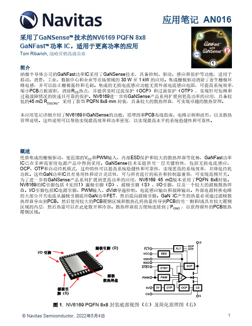
图1. NV6169 PQFN 8x8封装底部视图(左)及简化原理图(右)漏极引脚(D )I/O 引脚源极引脚(S )源极散热焊盘概述凭借集成的栅极驱动、宽范围的V CC 和PWM 输入、内部ESD 保护和较大的散热焊盘等优势,GaNFast 功率IC 已在多种高密度电源产品中得到采用。
GaNSense 技术还提供另一层关键特性,包括无损电流感应、OCP 、OTP 和自动待机模式,这些特性可以提高系统稳健性和可靠性,实现更高的系统效率,并降低待机功耗。
这些GaN 功率IC 具有易用性和设计灵活性,可与所有流行的拓扑和控制器兼容,可实现高频开关。
为了进一步将GaNSense 产品系列扩展到更高功率的应用,NV616945m Ω版本采用了PQFN 8x8封装。
NV6169的IC 引脚包括(见图1)漏极引脚(D )、源极引脚(S )、I/O 引脚、以及一个较大的源极散热焊盘。
I/O 引脚包括IC 电源引脚、PWM 输入、dV/dt 导通控制、电流感应输出和故障输出。
CY7C1069DV33 16Mb 静态 RAM 产品说明书

CY7C1069DV3316-Mbit (2M x 8) Static RAM
CypressSemiconductorCorporation•198 Champion Court•SanJose,CA95134-1709•408-943-2600Document Number: 38-05478 Rev. *D Revised September 06, 2007
Features■High speed❐tAA = 10 ns ■Low active power❐ICC = 175 mA at 10 ns■Low CMOS standby power❐ISB2 = 25 mA■Operating voltages of 3.3 ± 0.3V■2.0V data retention ■Automatic power down when deselected■TTL compatible inputs and outputs■Easy memory expansion with CE1 and CE2 features■Available in Pb-free 54-Pin TSOP II and 48-Ball VFBGA packagesFunctional DescriptionThe CY7C1069DV33 is a high performance CMOS Static RAMorganized as 2,097,152 words by 8 bits.
To write to the device, take Chip Enables (CE1 LOW and CE2
HIGH) and Write Enable (WE) input LOW. Data on the eight IO
pins (IO0 through IO7) is then written into the location specifiedon the address pins (A0 through A20).
高新兴物联ME3616 NB-IoT模组硬件用户指导手册说明书
:警告或注意:备注或说明目的明确的了解,并可在此文档基础上顺利完成无线通信上网类产品或设备的应用开发。
为了给用户提供一个较为全面的设计参考,此硬件开发文档不仅提供了产品功能特点和技术参数,还提供了产品可靠性测试和相关测试标准、业务功能实现流程、射频性能指标以及用户电路设计指导。
注意:为保证模组板在客户端的焊接直通率,确保该模组后续集成过程中的制造和焊接质量。
本文档中第七章内容提供SMT工艺和缩略语安全警告和注意事项在模组二次开发、使用及返修等过程中,都必须遵循本章节的所有安全警告及注意事项。
模组的集成商等必须将如下的安全信息传递给用户、操作人员或集成在产品的使用手册中:●在使用包括模组在内的射频设备时可能会对一些屏蔽性能不好的电子设备造成干扰,请尽可能在远离普通电话、电视、收音机和办公自动化的地方使用,以免这些设备和模组相互影响。
●在如助听器、植入耳蜗和心脏起搏器等医用设备旁使用包含模组的设备时,请先向该设备生产厂家咨询了解。
●请不要在油料仓库,化学工厂等有潜在爆炸危险的环境,或在医院、飞机等有特殊要求的场所,使用包含模组的设备。
●请不要将模组暴露在强烈日光之下,以免过度受热而损坏。
●本产品没有防水性能,请避免各种液体进入模组内部,请勿在浴室等高湿度的地方使用,以免造成损坏。
●非专业人员,请勿自行拆开模组,以免造成人员及设备损伤。
●清洁模组时请先关机,并使用干净的防静电布。
用户有责任遵循其他国家关于无线通信模组及设备的相关规定和具体的使用环境法规。
我司不承担因客户未能遵循这些规定导致的相关损失。
目录关于本文档 (I)安全警告和注意事项............................................................................................................................................................. I II 目录. (IV)表格索引 (VI)图形索引 (VIII)1. 产品概述 (10)1.1.整体概述 (10)1.2.关键特点 (10)1.3.模组框图 (11)2. 应用接口 (12)2.1.整体概述 (12)2.2.管脚分布 (12)2.3.管脚描述 (13)2.4.工作模式 (15)2.5.电源供给 (16)2.5.1. 电源管脚 (16)2.5.2. 减少供电电源压降 (16)2.5.3. 电源参考电路设计 (17)2.6.VCC1V8_OUT参考设计 (17)2.7.开机 (18)2.8.关机 (21)2.9.复位 (22)IM接口 (24)2.10.1. 管脚描述 (24)2.10.2. USIM卡座 (25)2.11.UART接口 (27)2.11.1. 串口连接 (27)2.11.2. 使用三极管做电平转化 (28)2.11.3. 使用电平转换芯片做电平转化 (32)2.12.状态指示 (34)2.13.ADC接口 (35)2.14.GPIO接口 (35)2.15.WAKEUP_IN接口 (35)2.16.WAKEUP_OUT接口 (36)B接口 (37)3. 天线接口 (38)3.1.管脚定义 (38)3.2.参考设计 (38)3.3.天线的PCB设计 (39)3.4.EMC和ESD设计 (39)3.4.1. EMC设计 (39)3.4.2. ESD设计 (39)3.5.天线OTA测试方法 (39)4. 电气、可靠性和射频特点 (41)4.1.工作温度 (41)4.2.工作电流 (41)4.3.RF输出功率 (42)4.4.RF接收灵敏度 (42)4.5.静电放电 (42)4.6.GNSS性能指标参数 (42)5. 封装尺寸 (44)5.1.模组尺寸 (44)5.2.推荐封装尺寸 (46)6. 测试和测试标准 (47)6.1.测试参考 (47)6.2.测试环境说明 (47)6.3.可靠性测试环境 (48)7. 贴片工艺和烘烤指导 (49)7.1.存储要求 (49)7.2.模组平面度标准 (49)7.3.工艺路径选择 (49)7.3.1. 锡膏选择 (49)7.3.2. 主板对应模组焊盘钢网开孔设计 (49)7.3.3. 模组贴片 (50)7.3.4. 模组焊接回流曲线 (52)7.3.5. 过炉方式 (52)7.3.6. 不良品维修 (52)7.4.模组烘烤指导 (53)7.4.1. 模组烘烤环境 (53)7.4.2. 烘烤设备和操作方法 (53)7.4.3. 模组烘烤条件 (53)表格索引表1-1ME3616支持频段 (10)表1-2ME3616关键特点 (10)表2-1 输入输出(IO)参数定义 (13)表2-2逻辑电平 (13)表2-3管脚定义 (13)表2-4电源供给 (16)表2-5 VCC1V8_OUT信号定义 (17)表2-6开关机信号管脚 (18)表2-7开机时间 (21)表2-8关机时间 (21)表2-9复位信号定义 (22)表2-10复位时间 (23)表2-11 USIM卡接口定义 (24)表2-12 Molex USIM卡座管脚描述 (25)表2-13 Amphenol USIM卡座管脚描述 (26)表2-14主UART接口定义 (27)表2-15调试UART接口定义 (33)表2-16网络指示灯管脚定义 (34)表2-17 ADC管脚定义 (35)表2-18 ADC接口特性 (35)表2-19 GPIO管脚定义 (35)表2-20 WAKEUP_IN定义 (35)表2-21 WAKEUP_OUT定义 (36)表3-1天线接口定义 (38)表4-1温度参数 (41)表4-2平均功耗 (41)表4-3平均功耗 (41)表4-4 RF输出功率 (42)表4-5 RF接收灵敏度 (42)表4-6 ME3616模组静电放电特征 (42)表4-7 GNSS性能指标参数 (42)表6-1测试标准 (47)表6-2测试环境 (47)表6-3测试仪器和设备 (48)表6-4可靠性测试参数 (48)表7-1烘烤参数 (49)表7-2 LCC模组焊盘钢网开孔 (50)图形索引图1-1系统链接框图 (11)图2-1管脚分配 (12)图2-2工作模式切换 (16)图2-3 VBAT输入参考电路 (17)图2-4 DC-DC参考电路 (17)图2-5 VCC1V8_OUT参考电路 (18)图2-6开关机参考电路 (19)图2-7上电开机参考设计 (20)图2-8模组开机时序 (20)图2-9模组POWER_ON唤醒时序 (21)图2-10 模组关机时序图 (22)图2-11复位参考电路 (23)图2-12模组复位时序图 (24)图2-13 USIM卡参考电路图 (24)图2-14 Molex 91228 USIM卡座 (25)图2-15 Amphenol C707 10M006 512 2 USIM卡座 (26)图2-16串口三线连接示意 (27)图2-17串口带流控连四线接示意 (28)图2-18 TXD电平匹配参考电路 (29)图2-19 RXD电平匹配参考电路 (30)图2-20 RTS电平匹配参考电路 (31)图2-21 CTS电平匹配参考电路 (32)图2-22 4线UART芯片电平匹配参考电路 (33)图2-23 2线UART芯片电平匹配参考电路 (33)图2-24调试UART接口引出测试点 (34)图2-25模组状态指示参考电路 (35)图2-26 WAKEUP_IN输入时序 (35)图2-27 WAKEUP_IN管脚外部连接示意图 (36)图2-28 WAKEUP_OUT输出时序 (36)图2-29 WAKEUP_OUT管脚外部连接示意图 (37)图2-30模组USB添加测试点参考电路设计 (37)图3-1天线接口参考电路 (38)图5-1 ME3616尺寸图(公差:±0.1mm) (44)图5-2 ME3616尺寸图(正面透视图) (45)图5-3推荐封装尺寸(单位:mm) (46)图7-1模组钢网示意图 (50)图7-2模组卷带包装 (51)图7-3模组卷带包装相关尺寸 (51)图7-4模组炉温参考曲线图 (52)1.产品概述1.1.整体概述ME3616是一款采用LCC封装的基于NB-IoT通信标准的移动通讯网络模组。
- 1、下载文档前请自行甄别文档内容的完整性,平台不提供额外的编辑、内容补充、找答案等附加服务。
- 2、"仅部分预览"的文档,不可在线预览部分如存在完整性等问题,可反馈申请退款(可完整预览的文档不适用该条件!)。
- 3、如文档侵犯您的权益,请联系客服反馈,我们会尽快为您处理(人工客服工作时间:9:00-18:30)。
HY016射频设计4-静态NV生成说明 HY016射频设计4_静态NV生成说明 在PCB投板的两周间隙中,射频工程师可以先把静态NV和校准文件准备起来。这样等板子贴片回来后就可以下载静态NV,验证原理图设计了。本文对静态NV进行介绍,并详细说明如何生成HY016的静态NV。 目前高通平台,绝大部分射频相关参数是通过NV来进行配置的。一份静态NV包括如下部分: 1、 硬件设计对应的RF Card(NV1878) 2、 射频电路支持的所有频段,包括2G/3G/4G,发射/主接收/分集接收 3、 每个支持频段的射频相关参数,包括发射和接收的增益等级、切换点、最大最小发射功率、温度补偿、时序控制等 一份正确的静态NV是要让射频电路跑起来的必要条件。
RF Card RF Card是硬件和驱动正确关联的关键。每份不同的硬件设计采用不同的RF Card,比如有些是WTR2965+QFE4373的,有些是WTR4905+QFE4320的,有些支持南美频段,有些支持国内CA。这些不同的硬件设计,都对应不同的RF Card。驱动则根据不同的RF Card对硬件做相应的配置。所以RF Card弄错,往往都会导致开机死机。 RF Card保持在NV1878中。以HY016南美全频段为例,射频和驱动约定这个设计的RF Card是111,即NV1878=111。在这个RF Card中,射频采用WTR4905+RDA PhaseII来实现南美全频段。驱动也需要在这个RF Card下修改代码,使之和硬件相匹配,重点是通过MIPI和GPIO对芯片的模式和频段进行控制。
若我们使用的是高通的参考设计,那高通会有默认原理图和驱动代码,我们只要沿用这份原理图的RF Card即可。 以8909 QCN_XTT_MBN_NV_sysRFCalDll_8909_JO.3.0_r00046为例,在软件代码如下路径中可以看到高通支持的RFCard QCN_XTT_MBN_NV_sysRFCalDll_8909_JO.3.0_r00046\modem_proc\rftarget_jolokia\msm8909\qcn(驱动每个基线都会把这部分文档上传到服务器)
但这些RF Card都是采用高通的PA进行设计的电路,在成本上会贵不少。所以我们采用新的射频方案后,往往第一个平台都要自己准备相关NV,PA厂家若能提供那就更好了。
RFC文件夹说明 以WTR4905_chile_srlte_V2为例来说明一个具体的RFC文件夹。打开这个文件夹能看到:
里面包括一个MasterFile的主文件和所有这个Card支持频段的参数。MasterFile中包括了所有这个Card支持的频段的索引,每个索引都代表外面文件夹中的一个文件。下图就是MSM8909_WTR4905_CHILE_SRLTE_V2_MASTERFILE.xml的前一部分:
如href="WTR4905_CHILE_SRLTE_V2_CDMA_BC0_RX0.xml#xpointer(/NvSource/*)"/> 就代表要导入WTR4905_CHILE_SRLTE_V2_CDMA_BC0_TX0.xml文件,即CDMA制式下850M频段的主发射通路相关射频参数。
MasterFile文件中除了每个频段的具体参数外,在最后还包括如下整个RFCard频段相关参数:
这两部分变构成了整个MasterFile文件 下图以LTE B1的发射、主接收、分集接收的文件为例,对主要NV进行说明 WTR4905_CHILE_SRLTE_V2_LTE_B1_TX0.xml WTR4905_CHILE_SRLTE_V2_LTE_B1_RX0.xml WTR4905_CHILE_SRLTE_V2_LTE_B1_RX1.xml HY016南美全频段静态文件的生成 HY016南美全频段需要支持:GSM QB+WCDMA B1/2/4/5/8+LTE B2/4/5/7/12/28A/28B 高通目前没有RDA PhaseII的RFCard,所以我们最快捷的方法是从F8T(国内电信全网通)的静态NV进行扩展。 首先修改频段等相关参数,包括RFCard。NV定义和修改说明如下图:
然后再添加新增频段的参数(需增加WCDMA B2/4/5, LTE B2/4/7/12/28A/28B),这里以增加LTE B12为例进行说明。 1, 在高通现有RFC中找一个支持B12的作为基本模板。 \qcn\wtr4905_tmo\etc包含B12,所以可以把这个文件夹下的三个文件作为模板进行删减优化 WTR4905_TMO_LTE_B12_TX0.xml WTR4905_TMO_LTE_B12_RX0.xml WTR4905_TMO_LTE_B12_RX1.xml
2, 先看两个简单的接收文件RX0和RX1 由于同为WTR4905为射频收发器,所以增益等级可以共用,即LNA共包括六个不同增益等级,各增益等级的上升下降沿如下: [-74dbm,-78dBm,-60dbm,-64dbm,-40dBm,-44dBm,-28dBm,-32dBm,-20dBm,-24dBm]
mapping="direct" encoding="dec">-740,-780,-600,-640,-400,-440,-280,-320,-200,-240,0,0,0,0,0,0,0,0,0,0,0,0,0,0,0,0,0,0,0,0,0,0 mapping="direct" encoding="dec">-740,-780,-600,-640,-400,-440,-280,-320,-200,-240,0,0,0,0,0,0,0,0,0,0,0,0,0,0,0,0,0,0,0,0,0,0
3, 然后看发射文件TX 由于我们的射频电路未采用APT或EPT模式,所以这些XPT相关NV可以直接删除 name="RFNV_LTE_B12_TX_LIN_VS_TEMP_VS_FREQ_P_IN_I"> name="RFNV_LTE_B12_TX_LIN_VS_TEMP_VS_FREQ_P_OUT_I">
表示发射校准信道,可以沿用默认值,我们在QSPR校准时设置的信道须在这16个校准信道中
name="RFNV_LTE_C0_B12_FBRX_GAIN_SWITCH_POINT_I">,忽略,保持默认值
,最大发射功率,保持23dBm默认值
name="RFNV_LTE_B12_TX_ROT_ANGLE_PA_STATE_I">,PA不同增益等级的相位补偿,和PA特性有关,保持默认值
name="RFNV_LTE_B12_PA_COMPENSATE_UP_DOWN_I">,PA不同增益等级切换时AGC的补偿,和PA特性有关,保持默认值 ,不同增益等级下的温度补偿值,对电路调试无影响,保持默认值。后续温度特性较差的话,可以做些补偿,通常用默认值不会有问题
,最大发射功率的温度补偿值,对电路调试无影响,保持默认值。后续温度特性较差的话,可以做些补偿,通常用默认值不会有问题
,非常关键的参数,由PA特性决定,对应[PA State0,State1,State2,State3]的控制逻辑。对于RDA PhaseII PA,只有两个增益等级,PA State0是3,对应低增益等级;State1-3都是0,对应高增益等级。默认值是基于QPA的,包含四个增益等级,是[3,2,1,0]。我们需要将其修改为[3,0,0,0]
,高增益切换到低增益等级AGC的保持时间,用默认值即可
name="RFNV_LTE_B12_PA_RISE_FALL_THRESHOLD_I">,PA增益等级切换点,和PA特性相关。换算规则是10*(70+dBm),须和PA_Range_Map对应。根据RPM6743的Datasheet,我们将切换点设置在[6.5dBm,3.5dBm],即 NV22153=<765,735,2047,2047,2047,2047,0,0,0,0,0,0,0,0,0,0
name="RFNV_LTE_B12_MPR_BASED_PA_SWITCHPOINTS_SHIFT_I">,忽略,保持默认值 ,发射功率回退,保持默认值 防止DAC饱和的功率回退值,保持默认值
name="RFNV_LTE_B12_TX_EPT_DPD_CONFIG_PARAMS_I">,由于我们未采用APT或EPT模式,所以第一位设置为0即可
,精度为0.1dB的最小发射功率设置,获得更高精度 ,精度为0.1dB的最大发射功率设置,获得更高精度
4, 至此整个B12频段的静态NV全部添加完毕。重复同样的工作,直到把所有支持的频段全部添加好,便生成整个HY016南美频段的静态NV。比如可命名为: HY016_static_SA_Whole_180508.xml