PL3366C-ASEMI电源管理IC规格书
英飞凌单片机选型

24 / 30/40
最多10 1 1 4 最多2 QFP 144 / 176
16 / 24
最多8 0 1 4 QFP 64/100 / 144 - 40°C to +125°C
16 / 24
最多6 0 1 4 QFP 100 / 144 - 40°C to +125°C
9 / 16
最多6 0 1 2 QFP 64 / 100
程序 [PSRAM]
数据 [DSRAM] 双端口[DPRAM]
SB RAM CAN ADC Standby 通道数 通道数 8 最多3 最多24 最多6 0 1 最多4 可选 QFP 100 / 144 - 40°C to +125°C
112
24 2 8 3 24 8 0 1 4 2 通道 QFP 144 - 40°C to +125°C
XC874
Vector Computer
XC878
Vector Computer
52kB
XC874
Vector Computer
XC878
Vector Computer
32kB
XC886
Vector Computer
XC888
Vector Computer
XC886
XC888
Vector Computer
工作温度 (T环境)
- 40°C to +125°C
- 40°C to +125°C
-40°C to +125°C
* **
USIC: CCU:
可配置成UART, LIN, SPI/QSPI, IIC, IIS 用于PWM, D/A
04.05.2012
XLSEMI XL8002 80V 1A高效降压PWM LED常电流驱动器说明书
80V 1A High Efficiency Buck PFM LED Constant Current Driver XL8002FeaturesOperation Voltage DC 12V~80V. 0.1V current sense voltage reference. Directly drive 1~18 Series 1W/3W LED. Excellent line and load regulation.Internal Optimize Power HV-MOSFET. Built in Thermal Shutdown Function. Built in Current Limiting Function.Built in Soft-Start Circuit.Available in TO263-5L package. Up to 98% efficiency. ApplicationsLED Lighting & LED LAMP General purpose LED lightingGeneral DescriptionThe XL8002 is a monolithic high voltage switching regulator with PFM that is specifically designed to operate from a 12V~80V DC power supply.The XL8002 is a high efficiency LED driver switching regulator. The LED string is driven at DC constant current rather than constant voltage, thus providing constant light output and enhanced reliability.Figure1. Package Type of XL800280V 1A High Efficiency Buck PFM LED Constant Current Driver XL800280V 1A High Efficiency Buck PFM LED Constant Current Driver XL8002Figure4. XL8002 Typical Application80V 1A High Efficiency Buck PFM LED Constant Current Driver XL8002Figure5. Efficiency VS Output N*1W LEDFigure6. Output ILED Load Regulation VS Output N*1W LED80V 1A High Efficiency Buck PFM LED Constant Current Driver XL800280V 1A High Efficiency Buck PFM LED Constant Current Driver XL800280V 1A High Efficiency Buck PFM LED Constant Current Driver XL8002 Figure7. XL8002 System Application at VIN=60V~80V Schematic Figure8. XL8002 System Application at VIN=60V~80V Efficiency Curve80V 1A High Efficiency Buck PFM LED Constant Current Driver XL8002 Figure9. XL8002 System Application at VIN=36V~60V Schematic80V 1A High Efficiency Buck PFM LED Constant Current Driver XL8002Figure10. XL8002 System Application at VIN=36V~60V Efficiency Curve Table2: Figure9 Input VIN=36V/48V system parameters table:80V 1A High Efficiency Buck PFM LED Constant Current Driver XL8002Figure11. XL8002 System Application at VIN=12V~36V SchematicFigure12. XL8002 System Application at VIN=12V~36V Efficiency CurveTable3: Figure11 Input VIN=12V/24V system parameters table:VIN=12V VIN=24VFOSC Pout Efficiency FOSC Pout Efficiency1.01W 82.3%1.96W 90.8%2.91W 94.1%47.25K 3.80W 95.5%42.17K 4.70W 96.6%31.13K 5.61W 97.2%80V 1A High Efficiency Buck PFM LED Constant Current Driver XL8002 Figure13. XL8002 System Application at VIN=60V~80V Schematic Figure14. XL8002 System Application at VIN=60V~80V Efficiency Curve80V 1A High Efficiency Buck PFM LED Constant Current Driver XL800280V 1A High Efficiency Buck PFM LED Constant Current Driver XL8002。
SMC EX260-SEC1 -SEC2 -SEC3 -SEC4 商品说明书
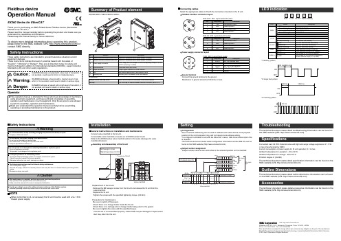
<EX260-SEC1/-SEC2/-SEC3/-SEC4>InstallationConfigurationAuto-increment addressing can be used to address each slave device via its physical position in the communication ring, and not require local address setting.To configure the EX260 SI unit with the EtherCAT master, XML Device Description File is required.The technical document states detail configuration information and the XML file can be found on the SMC website (.)Output number assignmentOutput number starts at zero and refers to the solenoid position on the manifold.General instructions on installation and maintenanceConnect valve manifold to the SI unit.Connectable valve manifolds are same as for EX250 series SI unit.Refer to the EX250 series valve manifold section in the valve catalogue for valvemanifold dimension.Power supply connector layoutGround terminalConnect the ground terminal to the ground.Resistance to ground should be 100 ohms or less.SettingReplacement of the SI unit•Remove the M3 hexagon screw from the SI unit and release the SI unit from the valve manifold.•Replace the SI unit.•Tighten the screws with the specified tightening torque. (0.6 Nm)Precautions for maintenance •Be sure to switch off the power.•Check there is no foreign matter inside the SI unit.•Check there is no damage and no foreign matter being stuck to the gasket.•Be sure to tighten the screw with the specified torque.If the SI unit is not assembled properly, inside PCBs may be damaged or liquid and/or dust may enter into the unit.Connecting cablesSelect the appropriate cables to fit with the connectors mounted on the SI unit.Fieldbus interface connector layoutTroubleshootingThe technical document states detail troubleshooting information can be found on the SMC website (URL )SpecificationsConnected load: 24VDC Solenoid valve with light and surge voltage suppressor of 1.5 W or less (manufactured by SMC)Current consumption of power supply for SI unit operation: 0.1 A max.Ambient temperature for operation: -10 to 50 ℃Ambient temperature for storage: -20 to 60 ℃Pollution degree 2: (UL508)The technical document states detail specification information can be found on the SMC website (URL )Akihabara UDX 15F, 4-14-1, Sotokanda, Chiyoda-ku, Tokyo 101-0021, JAPAN Phone: +81 3-5207-8249 Fax: +81 3-5298-5362URL Outline DimensionsThe technical document states detail outline dimensions information can be foundon the SMC website (URL )AccessoriesThe technical document states detail accessories information can be found on the SMC website (URL )*2: Single flash pattern*1: Blinking patternAssembly and disassembly of the SI unit*3: Flickering patternNOTEWhen conformity to UL is necessary the SI unit must be used with a UL 1310Class2 power supply.Fieldbus deviceOperation ManualEX260 Series for EtherCATThank you for purchasing an SMC EX260 Series Fieldbus device (Hereinafter referred to as "SI unit" ).Please read this manual carefully before operating the product and make sure you understand its capabilities and limitations.Please keep this manual handy for future reference.To obtain more detailed information about operating this product,please refer to the SMC website (URL ) or contact SMC directly.These safety instructions are intended to prevent hazardous situations and/or equipment damage.These instructions indicate the level of potential hazard with the labels of"Caution", " Warning" or "Danger". They are all important notes for safety and must be followed in addition to International standards (ISO/IEC), Japan Industrial Standards (JIS) and other safety regulations.OperatorNote: Specifications are subject to change without prior notice and any obligation on the part of the manufacturer.EtherCAT ®is registered trademark and patented technology, licensed by Beckhoff Automation GmbH, Germany.© 2010 SMC Corporation All Rights ReservedPWR: M12 5-pole Plug A-coded。
LMC-PCIE-V6K3-SPI 系列激光控制卡 电气使用说明书
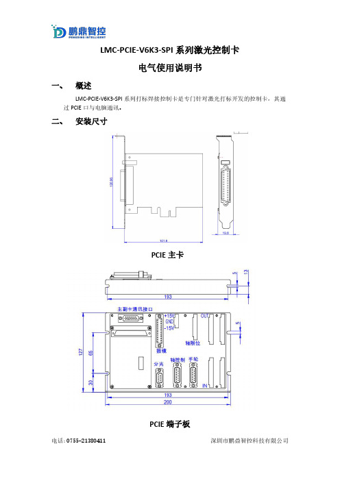
LMC-PCIE-V6K3-SPI系列激光控制卡电气使用说明书一、概述LMC-PCIE-V6K3-SPI系列打标焊接控制卡是专门针对激光打标开发的控制卡,其通过PCIE口与电脑通讯。
二、安装尺寸PCIE主卡PCIE端子板三、外观介绍PCIE主卡PCIE端子板四、LED指示灯说明注意:在对控制卡上电后第一时间查看亮灯情况,如果异常马上断电检查接线情况。
主卡灯状态:位号说明状态三色灯绿色指示灯空闲灯黄色指示灯运行灯红色指示灯报警灯端子板灯状态位号说明LED1负向电源指示灯LED6正向电源指示灯LED8外接24V电源指示灯(IO)LED3板卡空闲指示灯LED4板卡工作中指示灯LED5板卡错误指示灯五、接口说明5.1电源接口(J1,3PIN接线端子)5.1.1振镜不通过板卡J1端口供电接线方式管脚号板卡端丝印名称方向供电电源电压电源功率1+15V输入8V~28V>5W2GND输入GND3-15V不接注:如是以上方式接线,为避免振镜或板卡损坏需将振镜电源参考地与板卡电源参考地短接。
5.1.2振镜通过板卡J1端口供电接线方式管脚号板卡端丝印名称方向供电电源电压电源功率供电线径1+15V输入振镜正向电源电压(8~28V范围内)振镜功率+5W不小于0.75平方mm2GND输入GND振镜功率+5W不小于0.75平方mm 3-15V输入振镜负向电源电压(-8~-28V范围内)振镜功率+5W不小于0.75平方mm例如:鹏鼎Ⅰ、Ⅱ代振镜供电,J1端口如下接线:管脚号板卡端丝印名称方向供电电源电压电源功率供电线径1+15V输入+15V振镜功率+5W不小于0.75平方mm 2GND输入GND振镜功率+5W不小于0.75平方mm 3-15V输入-15V振镜功率+5W不小于0.75平方mm管脚号板卡端丝印名称方向供电电源电压电源功率供电线径1+15V输入+24V振镜功率+5W不小于0.75平方mm 2GND输入GND振镜功率+5W不小于0.75平方mm 3-15V输入不接5.2振镜控制接口定义(J3,DB25母头)(XY2-100协议接口定义)管脚名称说明信号方向管脚名称说明信号方向1Clk-时钟信号-输出14Clk+时钟信号+输出2Sync-同步信号-输出15Sync+同步信号+输出3X_data-X振镜信号-输出16X_data+X振镜信号+输出4Y_data-Y振镜信号-输出17Y_data+Y振镜信号+输出5X_fb-(A-)X振镜反馈-(复用,飞行A-)输入18X_fb+(A+)X振镜反馈+(复用,飞行A+)输入6Y_fb-(B-)Y振镜反馈-(复用,飞行B-)输入19Y_fb+(B+)Y振镜反馈+(复用,飞行B+)输入9/10 /22+15V振镜供电电源+15V输出,与J1的1脚直连11/23/24GND GND,电源参考点输出,与J1的2脚直连12/1 3/25-15V振镜供电电源-15V输出,与J1的3脚直连7/8/20/21NC留用5.2.1振镜控制接口(J3,DB25母头)(SL2-100协议接口定义)振镜接线(SL2-100)SCANLAB振镜接口控制卡振镜接口振镜管脚号振镜信号定义控制卡管脚号接口定义1DATA IN+16x-data+6DATA IN-3X-data-5DATA OUT+18X-FB+9DATA OUT-5X-FB-7,8GND11,23,24GND注:①振镜信号(+,-)为一对差分信号,信号线要用屏蔽双绞线,振镜信号线长度<20m.②如果振镜电源从J3供电,供电线缆线径不小于0.75平方mm。
微塞米ZL3066系列1-3通道10输入18输出线路卡时间IC产品简介说明书
ZL30661, ZL30662, ZL306631-, 2-, 3-Channel, 10-Input, 18-OutputLine Card Timing ICsProduct BriefAugust 2019 Features•One, Two or Three DPLL Channels•Programmable bandwidth, 14Hz to 470Hz•Freerun or holdover on loss of all inputs•Hitless reference switching•High-resolution holdover averaging•Per-DPLL phase adjustment, 1ps resolution•Programmable tracking range, phase-slope limiting, frequency-change limiting and otheradvanced features•Input Clocks•Accepts up to 10 differential or CMOS inputs•Any input frequency from 1kHz to 900MHz•Per-input activity and frequency monitoring•Automatic or manual reference switching•Revertive or nonrevertive switching•Any input can be a 1PPS SYNC input for REF+SYNC frequency/phase/time locking •Any input can be a clock with embedded 1PPS •Input-input phase measurement, 1ps resolution •Input-DPLL phase measurement, 1ps resolution •Per-input phase adjustment, 1ps resolution •Output Clock Frequency Generation•Any output frequency from <1Hz to 1045MHz (180MHz max for Synth0)•High-resolution fractional frequency conversion with 0ppm error•Synthesizers 1 & 2 have integer and fractional dividers to make a total of 5 frequency families •Output jitter from Synth 1 & 2 is <0.3ps RMS•Output jitter from fractional dividers is typically < 1ps RMS, many frequencies <0.5ps RMS •Each HPOUTP/N pair can be LVDS, LVPECL, HCSL, 2xCMOS, HSTL or programmable diff.•In 2xCMOS mode, the P and N pins can be different frequencies (e.g. 125MHz and 25MHz) •Four output banks each with VDDO pin; CMOS output voltages from 1.5V to 3.3V•Per-synthesizer phase adjust, 1ps resolution•Per-output programmable duty cycle•Precise output alignment circuitry and per-output phase adjustment•Per-output enable/disable and glitchlessstart/stop (stop high or low)•Local Oscillator•Operates from a single low-cost XO: 23.75-25MHz, 47.5-50MHz, 114.285-125MHz •High-stability applications can connect a TCXO or OCXO (any frequency, any output jitter) tothe OSCI pin to provide a stability reference •General Features•Automatic self-configuration at power-up from internal Flash memory•Input-to-output alignment <200ps (ext feedback) •Fast REF+SYNC locking for frequency and 1PPS phase alignment with lower-cost oscillator •Internal compensation (1ppt) for local oscillator frequency error in DPLLs and input monitors •Numerically controlled oscillator behavior in each DPLL and each fractional output divider•Easy-to-configure design requires no external VCXO or loop filter components•7 GPIO pins with many possible behaviors•SPI or I2C processor Interface• 1.8V and 3.3V core VDD voltages•Power: 1.3W for 2 inputs, 1 synth, 6 LVDS out•Easy-to-use evaluation/programming software Applications•Line card timing IC for SyncE, SyncE+1588, SONET/SDH, OTN, wireless base station andother systems carrier-grade systemOrdering InformationZL30661LFG7 1-Channel 80-lead LGA TraysZL30662LFG7 2-Channel 80-lead LGA TraysZL30663LFG7 3-Channel 80-lead LGA TraysNiAu (Pb-free)Package size: 11 x 11 mm-40︒C to +85︒C1. Block DiagramFigure 1 - Functional Block Diagram2. Application ExampleFigure 2 - Synchronous Ethernet and IEEE 1588 Line Card ApplicationFracDiv IntDiv FracDivIntDivHP Synthesizer 2low-jitterHPOUT6P HPOUT6N HPOUT7P HPOUT7NDIVREF0P DPLL0R S T _BC S _B _A S E L 0S C K _S C LS O _A S E L 1S I _S D AG P I O [8:0]Microprocessor Port SPI or I2C I/F & GPIO Pins One Diff / Two Single-Ended REF0N REF1P One Diff / Two Single-Ended REF1N REF2P One Diff / Two Single-EndedREF2NREF3P One Diff / Two Single-Ended REF3N REF4P One Diff / Two Single-EndedREF4NReference Monitors & State MachinesDPLL1DPLL2HP Synthesizer 1low-jitterGP Synthesizer 0general purpos eGPOUT0GPOUT1DIV DIVXO Optional x2O S C IO S C OMaster Clock M C L K I N _PDIVHPOUT4P HPOUT4N HPOUT5P HPOUT5N DIV DIVHPOUT0P HPOUT0N HPOUT1P HPOUT1N DIVDIV HPOUT2P HPOUT2N HPOUT3P HPOUT3NDIVDIVM C L K I N _NS R S T _BDPLL0Synth0DPLL1Synth1Synth22x 156.25MHz differential 2x 125MHz differential 25MHz CMOS 2x 155.52MHz, 161.1328125MHz or other frequencyto PHY transmitters, line card Ethernet switch IC, etc.from PHY receivers2x 156.25MHz differential 2x 125MHz differential 2x 25MHz CMOS2x 19.44MHz, 25MHzor 8kHz CMOS to central timing functionsfrom central timing functionsXO2x 19.44MHz or 25MHz CMOS1PPS CMOSoptional 2x 1PPS CMOSDPLL1 only present on ZL30662 and ZL30663 DPLL2 only present on ZL306633. Detailed Features3.1 Input Block Features•Ten input reference pins; each can accept a CMOS signal or the POS side of a differential pair; or two can be paired to accept both sides of a differential pair•Any input can be a SYNC signal for REF+SYNC frequency/phase/time locking•Any input can be a clock signal with embedded PPS signal (duty cycle distortion indicates PPS location) •Input clocks can be any frequency from 1kHz up to 900MHz (180MHz max for CMOS inputs)•Supported telecom frequencies include PDH, SDH, Synchronous Ethernet, OTN, wireless•Inputs constantly monitored by programmable frequency and single-cycle monitors•Single-cycle monitor can quickly disqualify a reference when measured period is incorrect•Frequency measurement (ppb or Hz) and monitoring (coarse, fine, and frequency-step monitors)•Optional input clock invalidation on GPIO assertion to react to LOS signals from PHYs•Input-to-input phase measurement, 1ps resolution•Input-to-DPLL phase measurement, 1ps resolution•Per-input phase adjustment, 1ps resolution3.2 DPLL Features•One, two or three full-featured DPLLs•Very high-resolution DPLL architecture•State machine automatically transitions among freerun, tracking and holdover states•Revertive or nonrevertive reference selection algorithm•Programmable bandwidth from 14Hz to 470Hz•Less than 0.1dB gain peaking•Fast frequency/phase/time lock capability for clock+1PPS input references•Programmable phase-slope limiting (PSL)•Programmable frequency rate-of-change limiting (FCL)•Programmable tracking range (i.e. hold-in range)•Truly hitless reference switching•Per-DPLL phase adjustment, 1ps resolution•High-resolution frequency and phase measurement•Fast detection of input clock failure and transition to holdover mode•High-resolution holdover frequency averaging•Time-of-Day registers: 48-bit seconds, 32-bit nanoseconds, writeable on input PPS edge3.3 Synthesizer Features•Any-to-any frequency conversion with 0ppm error•Two low-jitter synthesizers (Synth1, Synth2) with very high-resolution fractional scaling (i.e. non-integer multiplication)•Two output dividers per low-jitter synthesizer: one integer (4 to 15 plus half divides 4.5 to 7.5) and one 40-bit fractional•One general-purpose synthesizer (Synth0)• A total of five output frequency families•Easy-to-configure, completely encapsulated design requires no external VCXO or loop filter components3.4 Low-Jitter Output Clock Features•Up to 16 single-ended outputs (up to 8 differential outputs) from Synth1 and Synth2•Each output can be one differential output or two CMOS outputs•Output clocks can be any frequency from 1Hz to 1045MHz (250MHz max for CMOS and HSTL outputs) •Output jitter from Synth1 and Synth2 integer dividers is <0.3ps RMS•Output jitter from fractional dividers is <1ps RMS, many frequencies <0.5ps RMS•In CMOS mode, the HPOUTxN frequency can be an integer divisor of the HPOUTxP frequency (Example 1: HPOUT3P 125MHz, HPOUT3N 25MHz. Example 2: HPOUT2P 25MHz, HPOUT2N 1Hz)•Outputs directly interface (DC coupled) with LVDS, LVPECL, HSTL, HCSL and CMOS components •Supported telecom frequencies include PDH, SDH, Synchronous Ethernet, OTN•Can produce clock frequencies for microprocessors, ASICs, FPGAs and other components•Can produce PCIe clocks•Sophisticated output-to-output phase alignment•Per-synthesizer phase adjustment, 1ps resolution•Per-output phase adjustment•Per-output duty cycle / pulse width configuration•Per-output enable/disable•Per-output glitchless start/stop (stop high or low)3.5 General-Purpose Output Clock Features•Two CMOS outputs from Synth0•Any frequency from 1Hz to 180MHz•Output jitter is typically 20-30ps•Useful for applications where the component or system receiving the signal has low bandwidth such asa central timing IC•Can output a clock signal with embedded PPS (ePPS) (duty cycle distortion indicates PPS location) 3.6 Local Oscillator•Operates from a single low-cost XO (jitter reference for the device). Acceptable frequencies: 23.75MHz to 25MHz, 47.5MHz to 50MHz, 114.285MHz to 125MHz. Best jitter: ≥48MHz.•High stability applications can connect a TCXO or OCXO (any frequency, any output jitter) to a REF pin to provide a separate stability reference•This ability to have separate jitter and stability references greatly reduces the cost of the TCXO or OCXO (no jitter requirement, no high-frequency-requirement) and allows reuse of already-qualifiedTCXO and OCXO components3.7 General Features•Automatic self-configuration at power-up from internal Flash memory•Input-to-output alignment <200ps with external feedback•Fast REF+SYNC locking for frequency and 1PPS phase alignment with lower-cost oscillator•Generates output SYNC signals: 1PPS (IEEE 1588), 2kHz or 8kHz (SONET/SDH) or other frequency •JESD204B clocking: device clock and SYSREF signal generation with skew adjustment•Internal compensation for local oscillator frequency error in DPLLs and input monitors, 1ppt resolution •Numerically controlled oscillator (NCO) behavior allows system software to steer DPLL frequency or fractional output divider frequency with resolution better than 0.005ppt•Spread-spectrum modulation available in each fractional output divider (PCIe compliant)•Seven general-purpose I/O pins each with many possible status and control options•SPI or I2C serial microprocessor interface3.8 Evaluation Software•Simple, intuitive Windows-based graphical user interface•Supports all device features and register fields•Makes lab evaluation of the device quick and easy•Generates configuration scripts to be stored in internal Flash memory•Generates full or partial configuration scripts to be run on a system processor•Works with or without an evaluation boardMicrosemi Corporate Headquarters One EnterpriseAliso Viejo, CA 92656 USAWithin the USA: +1 (800) 713-4113 Outside the USA: +1 (949) 380-6100 Sales: +1 (949) 380-6136Fax: +1 (949) 215-4996E-mail: ***************************©2019 Microsemi Corporation. All rights reserved. Microsemi and the Microsemi logo are trademarks of Microsemi Corporation. All other trademarks and service marks are the property of their respective owners. Microsemi Corporation (Nasdaq: MSCC) offers a comprehensive portfolio of semiconductor and system solutions for communications, defense & security, aerospace and industrial markets. Products include high-performance and radiation-hardened analog mixed-signal integrated circuits, FPGAs, SoCs and ASICs; power management products; timing and synchronization devices and precise time solutions, setting the world’s standard for time; voice processing devices; RF solutions; discrete components; security technologies and scalable anti-tamper products; Power-over-Ethernet ICs and midspans; as well as custom design capabilities and services. Microsemi is headquartered in Aliso Viejo, Calif., and has approximately 3,400 employees globally. Learn more at .Microsemi makes no warranty, representation, or guarantee regarding the information contained herein or the suitability of its products and services for any particular purpose, nor does Microsemi assume any liability whatsoever arising out of the application or use of any product or circuit. The products sold hereunder and any other products sold by Microsemi have been subject to limited testing and should not be used in conjunction with mission-critical equipment or applications. Any performance specifications are believed to be reliable but are not verified, and Buyer must conduct and complete all performance and other testing of the products, alone and together with, or installed in, any end-products. Buyer shall not rely on any data and performance specifications or parameters provided by Microsemi. It is the Buyer’s responsibility to independently determine suitability of any products and to test and verify the same. The information provided by Microsemi hereunder is provided “as is, where is” and with all faults, and the entire risk associated with such information is entirely with the Buyer. Microsemi does not grant, explicitly or implicitly, to any party any patent rights, licenses, or any other IP rights, whether with regard to such information itself or anything described by such information. Information provided in this document is proprietary to Microsemi, and Microsemi reserves the right to make any changes to the information in this document or to any products and services at any time without notice.。
电子工程师常用的10款稳压元件
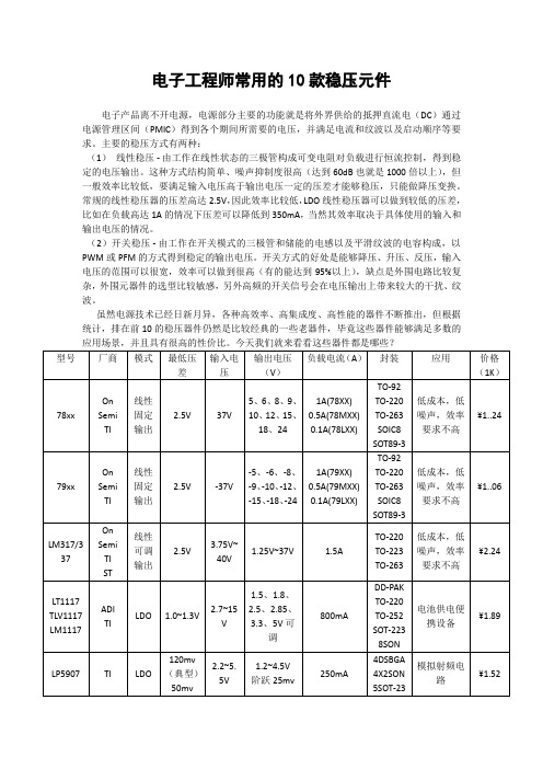
电子工程师常用的10款稳压元件电子产品离不开电源,电源部分主要的功能就是将外界供给的抵押直流电(DC)通过电源管理区间(PMIC)得到各个期间所需要的电压,并满足电流和纹波以及启动顺序等要求。
主要的稳压方式有两种:(1)线性稳压 - 由工作在线性状态的三极管构成可变电阻对负载进行恒流控制,得到稳定的电压输出。
这种方式结构简单、噪声抑制度很高(达到60dB也就是1000倍以上),但一般效率比较低,要满足输入电压高于输出电压一定的压差才能够稳压,只能做降压变换。
常规的线性稳压器的压差高达2.5V,因此效率比较低,LDO线性稳压器可以做到较低的压差,比如在负载高达1A的情况下压差可以降低到350mA,当然其效率取决于具体使用的输入和输出电压的情况。
(2)开关稳压 - 由工作在开关模式的三极管和储能的电感以及平滑纹波的电容构成,以PWM或PFM的方式得到稳定的输出电压。
开关方式的好处是能够降压、升压、反压,输入电压的范围可以很宽,效率可以做到很高(有的能达到95%以上),缺点是外围电路比较复杂,外围元器件的选型比较敏感,另外高频的开关信号会在电压输出上带来较大的干扰、纹波。
虽然电源技术已经日新月异,各种高效率、高集成度、高性能的器件不断推出,但根据统计,排在前10的稳压器件仍然是比较经典的一些老器件,毕竟这些器件能够满足多数的可以看成是78xx的夫妻档,经常配对使用。
78xx得到的是对地正电压,79xx得到的是对地负电压,除此之外跟78xx一样;3.LM317/LM117上面的78xx和79xx的器件输出电压是固定的,不可调整,LM317则是输出电压可以调节的线性稳压器,也有不同的封装支持不同的电流输出,最大输出电路可以高达 1.5A;也要求2.5v以上的压差才能正常稳压工作,也具备78xx一样的优点和缺点;4. 1117系列非常经典的LDO线性稳压器,相比于78xx和LM317系列的器件,它要求的输入电压和输出电压的差值为1.2V,因此可以广泛用在电池供电的便携式系统里面,比如通过4节1.25V 的电池(满电量的时候达到5V),电量不足到4.5V电压的时候依然能够通过1117-3.3得到3.3V的稳压输出供板子上的3.3V电路工作。
DDSI3366说明书(新)
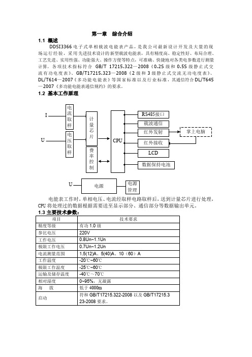
第一章 综合介绍 1.1 概述DDSI3366电子式单相载波电能表产品,是我公司最新设计开发及大量的现场运行经验,采用先进技术设计的新型载波电能表,具有精度高、稳定性好、布局合理、工艺先进、实用性强、功能强大、操作方便等特点,可准确、快捷地对各类电参数进行测量计算。
各项技术指标符合 GB/T 17215.322—2008《0.2S 级和0.5S 级静止式交流有功电度表》、GB/T17215.323—2008《2级和3级静止式交流无功电度表》、DL/T614—2007《多功能电能表》等国家标准以及行业标准,其通信符合DL/T645—2007《多功能电能表通信规约》的要求。
1.2 基本工作原理UU电能表工作时,单相电压、电流经取样电路取样后,送到计量芯片进行处理,CPU 将处理过的数据根据需要送至显示部分、通信部分等数据输出单元。
1.5 其他第二章仪表主要功能2.1 电能计量采用了24bit的高精度ΣΔ模数转换器,确保了采样的精度值,并保证了电能表在1000:1范围内的线性度优于0.2%。
同时对周边采样电路进行了优化设计,采用了大量的高精度高稳定性的电阻、电容、振荡器,确保电能表在-25℃至60℃的温度范围内误差偏移值优于国家相关标准。
如采用特殊工艺,电能表在10倍表的范围内可满足国标的计量要求。
a)具有正向、反向有功电能量计量功能,并可以据此设置组合有功和组合有功电能量。
b)具有分时计量功能;有功电能量应对尖、峰、平、谷等各时段电能量及总电能量分别进行累计、存储;c)具有单独计量正向有功、反向有功电能量计量功能,反向有功电能按正向有功电能单独进行计量和存储。
d)可测量有功功率、功率因数、电压、相电流、零线电流、电网频率、电表温度等运行参数。
2.2 时钟采用具有温度补偿功能的内置硬件时钟电路,具有日历、计时、闰年自动转换功能。
2.2.1 广播校时不受密码和硬件编程开关限制,对时钟误差小于或等于5分钟的电能表进行校时,每天只允许校对一次,且在午夜零点前后10分钟内不能进行广播校时。
美琴263585产品说明书
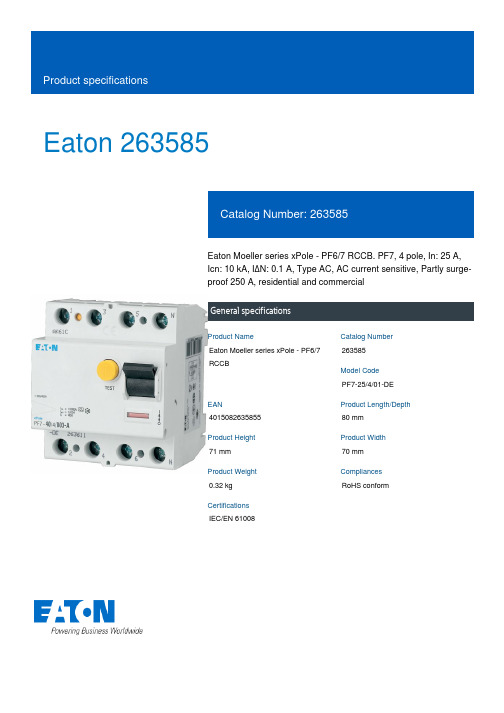
Eaton 263585Eaton Moeller series xPole - PF6/7 RCCB. PF7, 4 pole, In: 25 A, Icn: 10 kA, I ΔN: 0.1 A, Type AC, AC current sensitive, Partly surge-proof 250 A, residential and commercialGeneral specificationsEaton Moeller series xPole - PF6/7 RCCB263585PF7-25/4/01-DE401508263585580 mm 71 mm 70 mm 0.32 kg RoHS conformIEC/EN 61008Product NameCatalog Number Model Code EANProduct Length/Depth Product Height Product Width Product Weight Compliances Certifications25 AIs the panel builder's responsibility. The specifications for the switchgear must be observed.7035-35 °CMeets the product standard's requirements.Is the panel builder's responsibility. The specifications for the switchgear must be observed.DIN railQuick attachment with 2 latch positions for DIN-rail IEC/EN 6071525 ADoes not apply, since the entire switchgear needs to be evaluated.0.1 A184 V AC - 440 V ACMeets the product standard's requirements.Non-delayedIS/SPE-1TE 101911Interlocking device500 A eaton-rcd-application-guide-br019003en-en-us.pdfeaton-xpole-pf7-rccb-catalog-ca019032en-en-us.pdf eaton-xpole-pf6-rccb-catalog-ca019034en-en-us.pdfDA-DC-03_PF7eaton-circuit-breaker-xeffect-frcmm-rccb-dimensions.jpg eaton-xpole-pf6/7-rccb-3d-drawing.jpgIL019140ZUeaton-xeffect-frcmm-rccb-wiring-diagram-002.jpgRated operational current for specified heat dissipation (In) 10.11 Short-circuit ratingRAL-numberPermitted storage and transport temperature - min10.4 Clearances and creepage distances10.12 Electromagnetic compatibilityMounting MethodAmperage Rating10.2.5 LiftingRated fault current - maxTest circuit range10.2.3.1 Verification of thermal stability of enclosures Tripping timeFitted with:Rated residual making and breaking capacity Application notes Catalogs Certification reports DrawingsInstallation instructions Wiring diagramsFrequency rating50 Hz10.8 Connections for external conductorsIs the panel builder's responsibility.Fault current rating100 mATerminal protectionFinger and hand touch safe, DGUV VS3, EN 50274Special featuresMaximum operatingtemperature is 55 °C:Starting at 40 °C, the max.permissible continuouscurrent decreases by 3% forevery 1 °CTripping signal contact forsubsequent installation Z-NHK 248434Sensitivity typeAC current sensitiveAmbient operating temperature - max55 °CHeat dissipation per pole, current-dependent0 WClimatic proofing25-55 °C / 90-95% relative humidity according to IEC 60068-2Built-in depth69.5 mmShort-circuit rating63 A (max. admissible back-up fuse)FeaturesResidual current circuit breakerAdditional equipment possibleLifespan, electrical4000 operationsConnectable conductor cross section (solid-core) - min1.5 mm²10.9.3 Impulse withstand voltageIs the panel builder's responsibility.Number of polesFour-poleTerminal capacity (solid wire)1.5 mm² - 35 mm²Ambient operating temperature - min-25 °C10.6 Incorporation of switching devices and componentsDoes not apply, since the entire switchgear needs to be evaluated.Rated short-circuit strength10 kA10.5 Protection against electric shockDoes not apply, since the entire switchgear needs to be evaluated.Used withKLV-TC-4 276241 (Compact enclosure) Z-FW/LP 248296 (Remote control and automatic switching device) Z-RC/AK-4TE 101062 (sealing cover set)Residual current circuit breakersPF7Type ACKLV-TC-4 276241 (Compact enclosure)Z-FW/LP 248296 (Remote control and automatic switching device)Z-RC/AK-4TE 101062 (sealing cover set)Equipment heat dissipation, current-dependent2.8 W10.13 Mechanical functionThe device meets the requirements, provided the information in the instruction leaflet (IL) is observed.10.2.6 Mechanical impactDoes not apply, since the entire switchgear needs to be evaluated.10.9.4 Testing of enclosures made of insulating materialIs the panel builder's responsibility.Static heat dissipation, non-current-dependent0 WApplicationResidual current circuitbreaker for residential andcommercial applicationsxPole - Switchgear forresidential and commercialapplications10.3 Degree of protection of assembliesDoes not apply, since the entire switchgear needs to be evaluated.Voltage typeACTerminal capacity (stranded cable)16 mm² (2x)Leakage current typeACFrame45 mmBuilt-in width (number of units)70 mm (4 SU)Terminals (top and bottom)Open mouthed/lift terminalsHeat dissipation capacity0 WImpulse withstand currentPartly surge-proof 250 AWidth in number of modular spacings4Busbar material thickness0.8 mm - 2 mm10.2.3.2 Verification of resistance of insulating materials to normal heatMeets the product standard's requirements.10.2.3.3 Resist. of insul. mat. to abnormal heat/fire by internal elect. effectsMeets the product standard's requirements.Lifespan, mechanical20000 operationsVoltage rating230 V AC / 400 V AC10.9.2 Power-frequency electric strengthIs the panel builder's responsibility.Connectable conductor cross section (solid-core) - max35 mm²Degree of protectionIP20, IP40 with suitable enclosureIP20Rated short-time withstand current (Icw)10 kAAccessories requiredZ-HK 248432Pollution degree210.7 Internal electrical circuits and connectionsIs the panel builder's responsibility.Connectable conductor cross section (multi-wired) - min 1.5 mm²Rated impulse withstand voltage (Uimp)4 kV10.10 Temperature riseThe panel builder is responsible for the temperature rise calculation. Eaton will provide heat dissipation data for the devices.Connectable conductor cross section (multi-wired) - max 16 mm²TypePF7Residual current circuitbreakersType AC10.2.2 Corrosion resistanceMeets the product standard's requirements.10.2.4 Resistance to ultra-violet (UV) radiationMeets the product standard's requirements.10.2.7 InscriptionsMeets the product standard's requirements.Surge current capacity0.25 kAPermitted storage and transport temperature - maxEaton Corporation plc Eaton House30 Pembroke Road Dublin 4, Ireland © 2023 Eaton. All Rights Reserved. Eaton is a registered trademark.All other trademarks areproperty of their respectiveowners./socialmedia60 °C25 A gG/gL0.1 A400 V440 VAdmissible back-up fuse overload - max Rated fault current - min Rated operational voltage (Ue) - max Rated insulation voltage (Ui)。
- 1、下载文档前请自行甄别文档内容的完整性,平台不提供额外的编辑、内容补充、找答案等附加服务。
- 2、"仅部分预览"的文档,不可在线预览部分如存在完整性等问题,可反馈申请退款(可完整预览的文档不适用该条件!)。
- 3、如文档侵犯您的权益,请联系客服反馈,我们会尽快为您处理(人工客服工作时间:9:00-18:30)。
\/1.2 ©2020
I
< 乡
PL3366C
高精度恒流/恒压 原边控制PWM 功率开关
PM
ICRO
Powerlink Microelectronics
芯片概述:
PL3366C 是一款原边控制,用于反激式开关电源的恒流/恒 压调节器。
其高度集成了功率开关,并通过去除光耦以及次 级控制电路,在简化充电器/适配器等传统的恒流/恒压设计 的同时实现了精确的电流和电压调节,如图1所示。
PL3366C 的复合模式的应用使芯片能够实现低静态功耗、低 音频噪音、高效率。
满载时芯片工作在PFM 模式,随着负载 降低,芯片会逐渐进入到绿色模式,以提高整个系统的效率。
PL3366C 同时具有多种保护功能:逐周期峰值电流检测、 VDD 欠压/过压保护、输出过压保护、输出短路保护和过温 保护等。
Icc
图1典型的恒流/恒压波形
管脚分布图:
VDD 匚
「B 匚
,B
匚
CS 匚
2] GND
□ C □ C
PL3366C
1 概要
主要特点:
• 内置高压功率BJT 管
• 全电压范围内高精度恒流/恒压调节 • 去除光耦和次级控制电路 • 内置恒流调节的线电压补偿 • 内置变压器电感补偿 • 内置输出线补偿
• 内置可提高效率的自适应PFM 控制 • 低启动电流 • 内置前沿消隐 • 逐周期电流限制 • VDD 欠压/过压保护 • 输出过压保护 • 输出短路保护 •
内置过温保护
应用:
•手机充电器
・小功率率电源适配器
• LED 驱动
・消费类的备用电源
PL3366C是一款原边控制,用于反激式开关电源的恒流/恒压调节器。
其高度集成了功率开关,并通过去除光耦以及次级控制电路,在简化充电器/适配器等传统的恒流/恒压设计的同时实现了精确的电流和电压调节。
以提高整个系统的效率。
PL3366C具有多种保护功能以应对系统的各种异常状态。
主要包括:逐周期限流保护、VDD欠压/过压保护、输出短路/过压保护和过温保护等。
系统发生异常时,芯片将被保护,直到系统恢复正常状态。
PL3366C的复合模式的应用使芯片能够实现低静态
功耗、低音频噪音、高效率。
满载时芯片工作在PFM 模式,随着负载降低,芯片会逐渐进入到绿色模式,
2 特性
•内置高压功率BJT管
•全电压范围内高精度恒流/恒压调节
•去除光耦和次级控制电路
•内置恒流调节的线电压补偿
•内置变压器电感补偿
•内置输出线补偿PL3366C提供S0P7封装。
•低启动电流
•内置前沿消隐
•输出短路保护
•输出过压保护
•逐周期限流保护•VDD欠压/过压保护•过温保护
•内置可提高效率的自适应PFM控制
3 管脚分布图
管脚图如下图所示:
4 管脚描述
管脚名 描述
VDD 芯片电源输入
FB 通过电阻分压连接到辅助绕组,该管脚用于检测输出信号并调节芯片的怛流 CS 通过检测连接CS 到地电阻的电压来反映原边电感电流 C 功率BJT 的集电极,连接到变压器的一端 GND
芯片地
5 最大额定值
参数
符号 范围
单位 VDD 电压 VDD -0.3 至∣J VDDclamp
V CS 输入 CS -0.3 到 5
V FB 输入 FB -0.3 到 5 V 最大工作结温
Tjmax 150 ℃ 存储温度
Tsto
-55 到 150
℃
焊接温度(Soldering, 10secs)
Tlea 260
℃ 注释:超过最大额定值可能损毁潜件;超过推荐工作范围的芯片功能特性不能保证;长时间工作于最大额纪条件下可能会 影响器件的稳定性.
6 推荐工作条件
参数 数值 单位 工作温度 -40 - 105 ℃ 典型工作频率@满载
65
kHz
VDD
IB IB
CS E
E E E
口
GND
□ C □ C
PL3366C
7 结构框图
VDD
GND
8 电气特性
(无特殊说明,其测试条件为:VDD =21V∕ΓA = 25°C)。