推挽 升压 电路
推挽式电路
推挽式电路推挽式电路是一种常见的电子电路,其设计理念是采用传统的三极管、场效应管和功率 MOS 管多样化组合的方式,来实现高可靠性、高稳定性的控制。
在日常生活和工业生产中,推挽式电路被广泛应用于功率放大、开关等领域。
下面我们来分步骤阐述推挽式电路的工作原理,以及常见的组成方式。
一、推挽式电路的工作原理推挽式电路的工作原理是通过两个开关电路的交替工作来实现控制。
其中一个开关电路负责将信号从低电平变为高电平进行放大,这个开关电路叫做“驱动电路”;另一个开关电路则负责将信号从高电平变为低电平进行放大,这个开关电路叫做“负载电路”。
两个开关电路工作相互协调,实现推挽放大的效果。
二、推挽式电路的组成方式推挽式电路的组成方式多样,下面我们介绍三种比较常见的组成方式。
1.三极管推挽式电路三极管推挽式电路是一种基本的推挽式电路,主要用于工频音响产品的放大,其组成方式是采用NPN三极管和PNP三极管分别组成驱动电路和负载电路,实现信号放大。
2.场效应管推挽式电路场效应管推挽式电路也是一种常用的推挽式电路,主要用于高频率的放大控制电路中。
该电路的组成方式是采用两个N沟道场效应管或两个P沟道场效应管组成驱动电路和负载电路,实现信号放大。
3.功率 MOS 管推挽式电路功率 MOS 管推挽式电路是一种高性能的推挽式电路,主要用于高速开关控制电路中。
该电路的组成方式是采用两个N沟道功率 MOS管或两个P沟道功率 MOS 管组成驱动电路和负载电路,实现信号放大。
通过以上三种方式的组合,我们可以组成各种不同类型的推挽式电路,满足不同的控制需求。
总之,推挽式电路是一种广泛应用的电路,其工作原理简单,组成方式多样,可以根据不同的应用场景进行组合配置,实现不同的控制需求。
关于推挽升压电路准软开关的实验研究

关于推挽升压电路准软开关的实验研究
在48V以下的中小功率逆变器上,前级结构,多数采用推挽方案,主要是它电路成熟,成本相对比较低,但推挽升压电路有一个顽症,就是推挽功率MOS管上的尖峰问题,强烈的尖峰不但造成大量的谐波干扰,还会威胁到MOS管的安全。
而一旦出现尖峰,再加吸收回路一般效果不大,而只会大大降低电路的效率。
下图是我的2400W高频机,在接近满载时的前级D极波形,尖峰干扰多的很无奈。
在这种情况下,我一般不敢长时间让它工作,因为才80V耐压的管子,尖峰最高已经超过80了。
把前级整成准谐振式的实验,据说可以大大降低尖峰现象。
我也曾专门去找来一篇浙江大学一位教授的论文,但一看这论文,光计算公式就有三四页,要把这一大堆的公式研究懂,以我的能力,是不可能的事了。
尽管我在我的新的2000W的功率主板PCB上留了谐振电容的位置,但一直没有下决心去实验它。
最近,也是心血来潮,决定实验一下,当然,不可能先去研究公式了,而是先上机试了再说,只要不炸机。
第一步,我先在变压器次级上串进了一个224、630V的CBB电容,再看D极波形,开机,能工作,带600W左右的负载,结果波形的上方出现了一个凹陷,见下图:
第二步,再在原先的电容上并上一个224/630v电容,这个凹陷平了一些。
第三步,再并上二个224/630v电容,一共4个,凹陷基本没有了。
再看一下,这时的D极波形,也是600W负载:
又调了一下死区电阻,尖峰一点也没有了。
推挽电路工作原理

推挽电路工作原理
推挽电路是一种常见的功率放大电路,它主要由NPN型和PNP 型的晶体管组成,能够实现高效率的功率放大。
在本文中,我们将详细介绍推挽电路的工作原理,以及其在电子领域中的应用。
推挽电路的工作原理基于NPN型和PNP型晶体管的工作特性。
在推挽电路中,NPN型和PNP型晶体管交替工作,实现了对输入信号的放大和输出信号的驱动。
当输入信号为正半周时,NPN型晶体管导通,将信号放大并输出;而当输入信号为负半周时,PNP型晶体管导通,同样将信号放大并输出。
这样,推挽电路能够实现对输入信号的完整放大和输出,同时还能有效地消除交叉失真。
推挽电路在电子领域中有着广泛的应用,其中最常见的就是在功率放大器中的应用。
由于推挽电路能够实现高效率的功率放大,因此在音响设备、功放设备以及各类电子设备中都能见到其身影。
此外,推挽电路还常常用于马达驱动电路中,能够实现对马达的高效驱动,提高了系统的整体效率和稳定性。
除了功率放大和马达驱动外,推挽电路还常常用于各类开关电路中。
由于其能够实现高效的信号放大和输出,因此在开关电源、
逆变器等领域都有着广泛的应用。
推挽电路不仅能够提高系统的工作效率,还能够减小系统的功耗,提高系统的稳定性和可靠性。
总的来说,推挽电路作为一种常见的功率放大电路,在电子领域中有着广泛的应用。
其工作原理基于NPN型和PNP型晶体管的工作特性,能够实现高效率的功率放大和信号输出。
在功率放大器、马达驱动器以及开关电路中都有着重要的作用,为电子设备的性能提升和系统的稳定性提供了有力支持。
推挽电路的应用前景广阔,相信在未来的电子领域中会有更多的创新应用涌现。
一种推挽式直流升压电路的设计
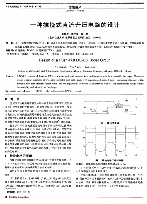
管 的 连 接 方式 分 有 单 端 式 、 桥 式 、 桥 式 和 推 挽 式 。 区 别 于 其 半 全
Q1
图 1 推 挽 式 电路
他不同的结构形式 , 推挽式 电路使用两个 开关管 , 并将 其连接 成
推 挽 功 率放 大器 形 式 。推 挽 电 路 的特 点 是 开 关 变 压 器 必 须 具 有
0 引 罱
T
直 流 升压 电路 是 逆 变 装 置 中的 一 项 十 分 重 要 的 环 节 , 发 展 其
水 平对逆变装置 的性 能起 到一定 的决定作 用。传统逆 变一般 采
用 先 逆 变 后 升 压 的方 式 , 本 高 、 成 电路 复 杂 、 试 困 难 且 波 形 质 量 调
t e fa i iiy a ei blt fte de in. h e sblt nd r la ii o h sg y
Ke w r s p s -u o v r D — C p l it m d l e P y o d :u hp l c n e C D u e dh o ua ( WM) ivr r l t sw t n et e
c ru ti mo e t a r i a yf b c i u t n h e u r me tfrd v c ’ p r mee si r lx d h x e me tlr s l o f m ic i s r h n o d n r y a k cr i a d te r q i l c e n o e i e a a t r s ea e .T e e p r n a e u t c n r S i s i
推挽电路工作原理详解
推挽电路工作原理详解推挽电路是一种常用的功率放大电路,它能够实现对信号的放大和输出,被广泛应用于音频功率放大器、电源放大器等领域。
推挽电路由两个互补的晶体管组成,通过它们的交替导通来实现对输入信号的放大和输出。
本文将详细解释推挽电路的工作原理,包括推挽电路的结构、工作过程和特点。
推挽电路的结构。
推挽电路由两个互补的晶体管组成,一个是NPN型的晶体管,另一个是PNP型的晶体管。
这两个晶体管的基极通过输入信号源相连,而它们的集电极则通过输出负载相连。
两个晶体管的发射极则分别通过电阻与电源相连,形成一个共集极的结构。
在推挽电路中,通常还会加入一个由两个二极管和一个电阻组成的偏置电路,用来对晶体管进行偏置,保证它们在工作时处于合适的工作状态。
推挽电路的工作原理。
当输入信号为正弦波时,首先对NPN型晶体管进行分析。
当输入信号为正弦波的正半周时,NPN型晶体管导通,此时PNP型晶体管截止。
这时,输出负载通过NPN型晶体管和电源之间的电阻得到电流,从而产生输出信号。
而当输入信号为正弦波的负半周时,NPN型晶体管截止,PNP型晶体管导通,输出负载同样通过PNP型晶体管和电源之间的电阻得到电流,产生输出信号。
通过这样的交替导通,推挽电路能够实现对输入信号的放大和输出。
推挽电路的特点。
推挽电路具有输出功率大、效率高、失真小等特点。
由于推挽电路中的NPN型和PNP型晶体管能够交替导通,因此输出功率可以是输入功率的两倍,这使得推挽电路在功率放大方面具有很大的优势。
同时,由于晶体管在导通时的电阻很小,在截止时的电阻很大,因此推挽电路的效率也很高。
此外,由于推挽电路能够实现对输入信号的放大和输出,因此输出信号的失真很小,能够保证输出信号的质量。
总结。
推挽电路是一种常用的功率放大电路,它由两个互补的晶体管组成,能够实现对输入信号的放大和输出。
通过两个晶体管的交替导通,推挽电路能够实现输出功率大、效率高、失真小等特点。
推挽电路在音频功率放大器、电源放大器等领域有着广泛的应用,是一种非常重要的电路结构。
单片机推挽开关升压逆变器程序

单片机推挽开关升压逆变器程序一、引言单片机推挽开关升压逆变器是一种常见的电路设计,可以将直流电源转换为交流电源,具有广泛的应用领域。
本文将详细介绍单片机推挽开关升压逆变器的程序设计原理和实现方法。
二、程序设计原理单片机推挽开关升压逆变器的程序设计原理主要包括以下几个方面:1. 时序控制:通过单片机的IO口控制推挽开关的开关状态,实现升压和逆变功能。
通过设定不同的开关状态和时间间隔,可以实现不同的输出电压和频率。
2. 脉宽调制:使用脉宽调制技术控制开关的导通和截止时间,从而控制输出电压的大小。
通常采用PWM(脉宽调制)技术,通过调节占空比来控制输出电压的大小。
3. 反馈控制:通过采集输出电压和电流的反馈信号,实现对输出电压和电流的精确控制。
可以采用PID控制算法,根据反馈信号与设定值之间的差异进行调节,使输出电压和电流稳定在设定值。
三、程序实现方法单片机推挽开关升压逆变器的程序实现主要分为以下几个步骤:1. 初始化:设置单片机的IO口为输出模式,并初始化相关的定时器和ADC模块。
2. 脉宽调制:根据需要的输出电压值,计算并设置相应的占空比。
通过改变占空比,可以调节输出电压的大小。
3. 时序控制:根据设定的开关状态和时间间隔,控制推挽开关的导通和截止。
通过改变开关状态和时间间隔,可以实现不同的输出电压和频率。
4. 反馈控制:采集输出电压和电流的反馈信号,并与设定值进行比较。
根据比较结果,调节脉宽调制的占空比,使输出电压和电流稳定在设定值。
5. 循环控制:将以上步骤放入一个循环中,实现持续的升压逆变功能。
通过不断的采集和调节,使输出电压和电流保持稳定。
四、总结本文介绍了单片机推挽开关升压逆变器的程序设计原理和实现方法。
通过合理的时序控制、脉宽调制和反馈控制,可以实现对输出电压和电流的精确控制。
这种逆变器具有简单、可靠、高效的特点,广泛应用于电力电子领域。
希望本文能对读者理解和应用单片机推挽开关升压逆变器提供一些帮助。
SG3525推挽式升压电路0001

SG3525隹挽式升压电路SG3525 推挽式升压电路2019-08-06 下午05:23ForewordThis contributed project is a result of considerable collaboration between Sergio and myself, and should not be seen as necessarily a complete project in itself, but a stepping stone to understanding switching power supplies, how they work, and what you can do with them.Be warned - there is considerable risk. Because of the extremely high current available from a car battery, a tiny mistake may easily lead to catastrophic failure. All electronic components are said to contain smoke (wire contains an enormous amount), and a slip of the soldering iron can liberate an unbelievable quantity. Seriously though, the risk of severe burns and the possibility of causing a fire in your car are very real, and should not be underestimated. 300A from a car battery can do a vast amount of damage in a few milliseconds - should the fuse not blow (you will use a fuse, won't you?), then the damage can be extensive.At various points in Sergio's part of the article, I have added some of my own information. This is shown in indented small font text.Please see the at the end of this article for important information about the project.IntroductionThe difficulties of installing an HI-FI system in a car are many, although there is no doubt that the most important is the limitation of the vehicle supply voltage. As most readers already know, the nominal voltage of a car battery is 12V, reaching about 13.8V when charging (i.e., engine running). The maximum RMS. audio power from a given voltage V is somewhat less than:Pmax = ( V / ( 2 x 2 ) )2 / RThus, for a 13.8V system, this power is limited to about 6W on a 4 Ohm load. Note that the lower the resistance of the speaker, the higher the maximum power (this is the reason most audio speakershave a 4 Ohm nominal impeda nee in stead of the more com mon 8 Ohm in home systems).This may be simplified to some exte nt ...P = (V / 3)2 / RLand a typical calculati on based on a 13.8V supply givesP = (13.8 / 3)2 / 4P = 4.62 / 4 = 5.29 WattsThis allows for sta ndard losses, and is acceptably accurate at this voltage - the only real way to know is to measure the amp, since the losses vary depe nding on the topology of the output stage inparticular.Power output can be in creased by a factor of n early 4 by using bridgi ng tech niq ues, expla ined in more detail in ESP project 14, so we can obtai n up to about 24W on a 4 Ohm speaker. This can be eno ugh for the midra nge and high freque ncies, but is obviously very limited for a subwoofer applicati on, for example. (moral: distrust of "4 x 45W" head un its is well advised, for they certai nly aren't talki ng about RMS power).So, what can be done to in crease available audio power? The an swer is a simple derivati on of the above formula - either decrease load impeda nee or in crease supply voltage. The lower the impeda nee, the more curre nt is n eeded, making the con structi on of low impeda nee output stagesmore difficult (there are some other practical limits), so let's in crease supply voltage.Switch Mode Power Supply BasicsThe vast majority of high-powered audio amplifiers use SMPS (Switch Mode Power Supplies) to gen erate higher voltages from the available 12 (13.8) volts. An exte nsive theoretical expla nati on on how these thi ngs work is bey ond the scope of this article, but these are some fun dame ntal ideas youshould know about switch mode power supplies (SMPS) for car amps:The DC voltage at the battery has to be switched in some form to gen erate an ACwaveform suitable for a tra nsformer. As you already know, a tran sformer basically con verts the AC voltage in its "primary" to a scaled versi on of it in its "sec on dary", the scale factor being the turns ratio of the primary to the sec on dary . (Agai n, take this as an extreme simplificati on). A tran sformer does n't allow DC voltages to pass, and there is electrical (galva nic) isolati onbetwee n both windin gs.The AC waveform is usually a square wave that is relatively easy and efficie nt to gen erate. The freque ncies usually fall betwee n 25kHz and 100kHz or more, thus allowi ng smaller tra nsformers tha n the used in main applia nces (its con struct ion is also differe nt, their cores are not lam in ated, but made from ferrites or "iro n powder"). The switchi ng eleme nts have to be capable of high curre nts and must also be fast and have low switchi ng losses. Usually, power MOSFETs or high speed bipolar tra nsistors are used (some SMPS desig ns use SCRs but theseare in the min ority).Once this waveform is stepped-up by the tra nsformer, it has to be rectified aga in and filtered back to DC, since that is what we want. For audio applicati ons, we usually n eed a symmetrical supply, +/-35V, for example. The rectificati on is done with a diode bridge, as it would be using a conven ti onal tran sformer at 50 or 60 Hz. Note that for the freque ncies we aretalk ing about, fast or ultra-fast diodes are n eeded.If we n eed a regulated power supply, some kind of feedback must be provided from the output rails to a con troller that can cha nge some parameters of the AC waveform at the primary of the tran sformer. This is n ormally accomplished with PWM (pulse width modulatio n). Wewill explai n this later, i n the "regulati on" paragraph.Always keep in mind that no en ergy is created …give n a (total) railsto battery voltages ratio, the curre nt draw n from the output will be (at least) be multiplied at the 12V in put by the same ratio, thus the total power stays the same (assu ming 100% efficie ncy, and that is n ever the case). A gen eric tran sformer "tra nsforms" the voltage by a factor of Tr, curre nt by a factor of 1/Tr, and impeda nee at the sec on dary by a factor of1/sqr(Tr), Tr being the turns ratio.Impeda nee is of little importa nee in this con text.A well built SMPS can reach 90% effieie ncy. So, if you expect to produce +/-35V at 6A (per rail) supply (this supposes 35x6 + 35x6=360W) the n be prepared to draw more tha n 30A from the battery! Fort un ately, whe n talk ing about audio amps reproduc ing music, powerrequireme nts are always much lower tha n with pure sine waves.At this point, the reader should realise the magn itude of the curre nts in volved in a high power SMPS for a car amplifier, and that extreme cauti on should be take n especially whe nconnecting "thecreature" to the car electrical system.The systemThe prese nt project describes the con struct ion of a flexible SMPS capable of deliveri ng powers in the order of 350W continu ously, depe nding on the tran sformer used. The output voltage depe nds mainly on the tur ns ratio of the primary and sec on dary windin gs, but may be adjusted to a somewhat lower value using regulati on. This should be eno ugh to power a 200W subwooferamplifier plus perhaps 2 stereo amps for the mids and highs.It is part of a complete car amp that I have built, with 6 power stages based on Nati onal's LM3886 Overture Amplifier. They can be comb ined into one >250W/4 Ohm subwoofer cha nn el plus 2 x 65W/4 Ohm mid+high cha nn els, alter natively into 2 x 120W/4 Ohm + 2 x 65W or even to form a multicha nnel 6 x 65W/4 Ohm amplifier, so it is an extremely flexible and high-powered system without renouncing sound quality. The parallel bridgi ng tech niq ues n eeded to do this will bepossibly described in ano ther project.Co nstruction of the SMPSThe complete schematic of the SMPS is show n below.Note: This is Sergio's origi nal vers ion of the supply, the one show n in is likely to be the most com monly used, as it is somewhat simpler, but has virtually ide ntical performa nee.[esp]Figure 2 - Switchmode Controller SchematicThere are three main blocks described below ...A - Switching MOSFETs and transformerB - Rectification and filteringC - Control circuitryA - Switching MOSFETs and TransformerThe selected switching topology is called a "push-pull" converter, because the transformer has a double primary (or a "centre-tapped" one, if your prefer). The centre tap is permanently connected to the car battery (via an LC filter to avoid creating peaks in thebattery lines, which could affect other electronic equipment in the car). The two ends of the primary are connected to a pair of paralleled MOSFETs each that tie them to ground in each conduction cycle (Vgs of thecorresponding MOSFET high).These MOSFETs should be fast, able to withstand high currents (in excess of 30A each if possible)and have the lowest possible Rds(on). The proposed On- Semiconductor ' s MTP75N06 canwithstand 75Amp and has a Rds(on) below 10 milliohm. This is important, because the lower this resistance is, the less power they are going to dissipate when switching with a square waveform.Another alternatives are MTP60N06, or the more popular BUZ11 and IRF540.Although the schematics show a previous bipolar push-pull stage, you can also connect the gate resistor directly to the output of the controlling IC, leaving out the transistors, as the SG3525 is capable to drive up to 500 mA (theoretically), more than enough to switch the MOSFETs fast.B - Rectification and FilteringIf one looks to the secondary side of the SMPS, it resembles exactly the scheme of a typical mains PSU, with one fundamental difference - the switching diodes have to be FAST or ULTRAFAST, if you use a standard diode bridge the system will simply blow up (and this can be very impressive, believe me!)Although a diode bridge is represented, it can be made with discrete diodes as well. Use high current (10 A minimum and a suitable voltage rating) diodes. I recommend using 4 xTO220 double diodes that can be paralleled to form a single one in each package.You may be surprised that the capacitors aren't too big. This is due to the high switching frequency. It is important that they are good quality ones and must be rated for 105 degrees operation. Ripple current rating and low ESR (equivalent series resistance) is very important for any switchingsupply. In my opinion, 5000uF per rail is enough.C - Control CircuitryThe controller IC is an SG3525. It comprises all the necessary subsystems to generate a fixed frequency, compare with a reference to modulate its pulse width and drive two outputswithout overlapping. It works from 8 to 35V and filtering in the supply is recommended, as shown. As stated above, you can connect the outputs directly to the gate resistors of the MOSFETs if you don'twant to include the bipolar stages.The resistor RT and capacitor CT fix the oscillation frequency.Experimentation showed me that about 35kHz produces good results with my transformer. Another capacitor, Css fixes the "slow start" time - when you turn on the system, the pulse width increases from 0 up to the steady value, thus limiting the "inrush" current, a very good feature to avoid "thumps" in the speaker and protect the electrical installation. It has also a shutdown pin that allows control of the SMPS from anexternal signal (REMOTE from the head unit, for example).In this project, layout is critical, incorrect track widths or excessivelylong traces can have high inductances and produce peaks that can make the MOSFETs blow up. ESP will probably offer asuitable PCB layout if there is enough interest in it.Transformer Construction DetailsThis is the most critical part of the design, and you have two options, buying a commercial unit with the required power rating and turns ratio (hard to find, only a single supplier found at the timeof writing), or wind your own.If you choose to wind your own transformer (as if you have much choice), you have to decide which shape of core to use. The preferred material is ferrite, which has high permeability (ability to "conduct" magnetic flux) or iron powder, which has a lower permeability, but is less likely to saturate. Most commercial transformers use ferrite, and iron powder is generally the best materialfor filter chokes (inductors) that carry substantial DC.For example, with a standard ETD39 core you could theoretically build a > 350W supply. Winding this type of cores is not very difficult, but you will have to follow some guidelines I provide belowwithstand 75Amp and has a Rds(on) below 10 milliohm. This is important, because the lower this resistance is, the less power they are going to dissipate when switching with a square waveform.Another alternatives are MTP60N06, or the more popular BUZ11 and IRF540.Although the schematics show a previous bipolar push-pull stage, you can also connect the gate resistor directly to the output of the controlling IC, leaving out the transistors, as the SG3525 is capable to drive up to 500 mA (theoretically), more than enough to switch the MOSFETs fast.B - Rectification and FilteringIf one looks to the secondary side of the SMPS, it resembles exactly the scheme of a typical mains PSU, with one fundamental difference - the switching diodes have to be FAST or ULTRAFAST, if you use a standard diode bridge the system will simply blow up (and this can be very impressive, believe me!) Although a diode bridge is represented, it can be made with discrete diodes as well. Use high current (10 A minimum and a suitable voltage rating) diodes. I recommend using 4 xTO220 double diodes that can be paralleled to form a single one in each package.You may be surprised that the capacitors aren't too big. This is due to the high switching frequency. It is important that they are good quality ones and must be rated for 105 degrees operation. Ripple current rating and low ESR (equivalent series resistance) is very important for any switchingsupply. In my opinion, 5000uF per rail is enough.C - Control CircuitryThe controller IC is an SG3525. It comprises all the necessary subsystems to generate a fixed frequency, compare with a reference to modulate its pulse width and drive two outputs without overlapping. It works from 8 to 35V and filtering in the supply is recommended, as shown. As stated above, you can connect the outputs directly to the gate resistors of the MOSFETs if you don'twant to include the bipolar stages.The resistor RT and capacitor CT fix the oscillation frequency.Experimentation showed me that about 35kHz produces good results with my transformer. Another capacitor, Css fixes the "slow start" time - when you turn on the system, the pulse width increases from 0 up to the steady value, thus limiting the "inrush" current, a very good feature to avoid "thumps" in the speaker and protect the electrical installation. It has also a shutdown pin that allows control of the SMPS from anexternal signal (REMOTE from the head unit, for example).In this project, layout is critical, incorrect track widths or excessivelylong traces can have high inductances and produce peaks that can make the MOSFETs blow up. ESP will probably offer asuitable PCB layout if there is enough interest in it.Transformer Construction DetailsThis is the most critical part of the design, and you have two options, buying a commercial unit with the required power rating and turns ratio (hard to find, only a single supplier found at the timeof writing), or wind your own.If you choose to wind your own transformer (as if you have much choice), you have to decide which shape of core to use. The preferred material is ferrite, which has high permeability (ability to "conduct" magnetic flux) oriron powder, which has a lower permeability, but is less likely to saturate. Most commercial tran sformers use ferrite, and iron powder is gen erally the best materialfor filter chokes (in ductors) that carry substa ntial DC.For example, with a sta ndard ETD39 core you could theoretically build a > 350W supply. Winding this type of cores is not very difficult, but you will have to follow some guideli nes I provide belowin order to have good results.Ano ther possibility is using a toroid. You can extract it from a BIG power in ductor. As a guide, a 4cm diameter toroid with a sect ion of about 1cm2 can be used for a > 250W SMPS. Winding is alittle bit more complicated tha n with ETD cores but with a little practice is not too difficult either.Toroidal coresETD-type coresToroid from ITL 100 in ductor (Wilco Corp).(Remove the thick wire before winding!:-)These are a few gen eral wi ndi ng guideli nes for all types of cores:You MUST use en amelled copper wire for all the windin gs. Keep also in mind that whe n work ing with high freque ncies, the effective secti on of the wire is much smaller tha n the physical one, due to the "ski n" effect (the curre nt concen trates only in the outer part of the wire). As high curre nts are in volved here, the sect ion of the wire is very importa nt, (if you don't want the en amel to fuse due to the heat ing produced by the resistive losses ofthe wire and short all the windin gs). A good practice is to use several thi nner wires in parallel rather tha n a sin gle thick one. This also eases winding. For example, six 0.4mm diameter wires can form a suitable primary for a 300W supply. The same applies to the sec on dary, although the curre nt is reduced so you can use less wires (3 or 4, for example). From now on, I will refer to each compositewire as "windin g", and to each thi n wire as "wire".The wires must be tightly wound. You must wind the primary first, trying to cover all thesurface of the core, and the n the sec on dary over it in the opposite directio n, to maximisein ter-w inding coupli ng.A good start ing point is using 4 tur ns for each primary (that is, 4turns, centre tap and ano ther 4 turns IN THE SAME DIRECTION). To calculate the nu mber of tur ns of thesec on dary winding, multiply by the tur ns ratio. For example, if you want to build a +/-30V supply, the tur ns ratio is 30/13.8=2.2 approx, so wi nd 2.2 x 4 = 8.8 tur ns (better 9 tur ns, to overcome the diode losses) for each sec on dary (that is, aga in, 9 tur ns, centre tap and ano ther 9turns IN THE SAME DIRECTION).To start winding, take the nu mber of thi n wires you have decided to use(6, for example) in the primary, all together. Leave about 3 or 4 cm out of the core to ease conn ecti on to the board and start winding. Whe n you have wound 4 COMPLETE tur ns, go out the core and cut at 3 or 4 cm. Now you have the first primary. The n start again IN THE SAME DIRECTION wi ndi ng the other 4 turns and at the end leave ano ther 3 or 4 cm for conn ecti on. Twist together the thinwires of each winding at the en ds, to ease solderi ng.The varnish of the wire is inten ded to provide electrical isolati on, so you have to remove it at the ends to make the connections to the board. Be sure to remove about 1cm to the end in ALL the wires you use. You can do that using a special solve nt or with san dpaper and a lot ofpatie nee BEFORE wi nding.The follow ing are photos of two models of tra nsformers. The left one is a toroidal I wound myself using the core from a big in ductor from Wilco Corporati on (ITL-501), and theright one is acommercial unit from a US manu facturer (2x3:1,350W). Both worked similarly.Left - Home Made Tran sformer. Commercial Tran sformer - RightOther remarksThe relay allows disc onn ect ing of the power supply with the REMOTE (or "Electrical Antenna" from the head un it. Power con sumpti on whe n off is the n only the gate curre nts of the MOSFETs (A few nA) and the base curre nt of the tran sistor that con trols the relay (a few uA).Nothi ng to worry about, certai nly.Connect a big choke in series with the supply, as this will elim in ate the switchi ng no ise that could in terfere with other electrical equipme nt. You can use the toroid that filters the +5Voutput of a old PC supply. (see figure below)My system's in put choke, obta ined from an old PC power supply.All the wiri ng, especially the primary side must be heavy gauged, in order to mini miselosses and avoid over-heati ng of the con ductors. The PCB tracks should be thick eno ugh, as short as possible, and rein forced with a gen erous tin layer and possibly with soldered wire. Put two fuses in the rails outputs, asthey can save you a lot of headaches whe n you shortthem to ground, etc. I used two sta ndard 6.3A fuses.Mount the rectifier diodes and the MOSFETs on a dece nt heats ink, and keep in mind that they must be electrically isolated. Follow the usual heats ink moun ti ng recomme ndati ons(thermal grease, etc.). TO220 packages are easy to han dle.Detail of the MOSFET arran geme ntNote the in sulati on pad (one for all) and the thick supply wires.In dividual in sulati on pads may be used with no loss of performa nee. Use of a clampi ng bar will give improved thermal con duct ion tothe heats ink bracket, but do not over tighte n, or the bracket will bend.TestsThis project han dles quite large powers, so it is well worth the pain of step-by-step testi ng beforeyou regret blowi ng all your work up in a microsec ond.For the tests, use a big 12V to 13.8V power supply, with curre nt limit ing if possible and capable of deliveri ng at least 10 to 20 amperes (see project 77). If you don't have that, a PC computer PSU will work (although you won't get more tha n 80-90W, but it is eno ugh for testi ng purposes and almost in destructible). Don't connect the SMPS to a car battery the first time you test it (it can be really dan gerous!). A 10A fuse in series with the 12V supply is also a good idea. (You don't know to whatexte nt!;-)The cables from the supply to the amp should be as short as possible and heavy gauged, to mini mise losses. First time I tested the amp I had a 1 volt of differe nee from one side to the cable to the otherin only 1.5 metres: the cable itself was dissipat ing more tha n 15W!!!. So, whe n calculat ing efficie ncy, always measure in put voltage just at the in put of the SMPS to accou nt for this. First of all, with only the SG3525 chip andits associated comp onents (no MOSFETs), check that you have a very clea n 12V square wave in each output (180o out of phase and they do not overlap EVER). Check also that whe n you tur n-o n the power, it starts from 0% to 50% duty cycle in about a sec ond or two.Once you have this, you can mount the MOSFETs. Do it on a heats ink, but be aware that the tabs are conn ected to the Drain, so provide in sulati on (mica + plastic washers, the usual stuff). Then solder the tran sformer and watch the primary waveform with an oscilloscope (use a 10:1 probe just in case you have large spikes in order to avoid damagi ng the in strume nt). You should have a square wave of about 25-26V peak to peak and the smallest peaks (overshoot) as possible. It they are higher tha n 30V (from groun d), you may try to re-wi nd the tran sformer to improve coupli ng. You can also reduce the overshoots using the snu bber n etwork show n in the schematic, although they will dissipate a bit of power (use 2W resistors and 100V capacitors),so mount them only if n ecessary.Once you have a clea n waveform, you can solder the rectifier and output capacitors and see what you have in the positive and n egative rails. You should have the same voltage in both, andit should be similar to what you calculated.Now try to load it with power resistors. Start with low power con sumpti on (about20W) and observe the mosfets, rectifiers and tran sformer carefully to see that they don't heat up. Also watch the curre nt draw n from the 12V supply. The power (V x I) should be only a bit highertha n that at the output load. (Expect a 80% efficie ncy or so).If everythi ng goes well, in crease the load (decrease its resista nee value). The mosfets should get warm after a while with heavy loads (about 100W), and the efficie ncy shouldmaintain high (always above 75-80%).Whe n you are completely sure that everythi ng works as expected, you can proceed to connect it to the car electrical wir ing (see "in stallati on procedures" paragraph). First time you will no tice an spark due to the sudde n charge of the big in put capacitor, uni ess you connect a resistor in series first(very good practice) to allow it charg ing slowly and the n remove it for no rmal operati on.In stallati on proceduresFor your car and own safety, it is VERY IMPORTANT that you pay special atte nti on whe n in stalli ng the power supply (and amplifier) in your car. These are some recomme ndati ons thatevery one should follow carefully:The supply MUST be take n directly from the battery, not to the radio or other +12V cables, as you will just blow or bur n them, with the risk of a fire in the car. The supply wire must be ofadequate sect ion, about 5 mm diameter (excludi ng the plastic cover) mi nimum.A fuse MUST be conn ected in series with the supply wire, as n ear the battery as possible, because otherwise, in case of a collisi on, the wire can be shorted to ground, which WILL produce a fire. This is not a joke! The battery can produce in excess of 300 A that can bur nvirtually any thi ng in a fract ion of a sec ond.Ano ther fuse should be put at the +12V in put of the amplifier, i n order to protect it from over curre nt. My recomme ndati on is to put a smaller value than the defi nitive and test the ampfor a few days to see if it overheats, etc. For example, a 10-15A fuse can be suitable.The FIRST conn ecti on you have to make to the amp is Ground, and that must be firmly screwed to the car chassis as n ear the amp as possible with thick wire. Notice that, if you conn ected, for example, the sig nal RCA cables first and then the +12V wire, the in putcapacitors would try to charge returni ng to ground via the audio cables, possibly ruining thepreamplifier of the head un it.Regulat ing the Power SupplyThe project itself has excelle nt load regulati on, and the rails voltage is almost only determ ined by the tur ns ratio, but it has in here ntly zero line regulati on (basically, it "simply" multiplies the in put voltage by the tur ns ratio), although this is not a problem in a car, where the battery voltage remai nsesse ntially con sta nt.If the obta ined output voltages are very high and you can't (or don't want to) modify the windin gs, you can use regulati on to lower them a bit. For example, I use a 3:1 tra nsformer that would give about +/-38V without regulati on that is un acceptable for my LM3886 stages to be safe, so I have regulated to +/-26V. The MOSFETs will suffer more, however, so regulate the supply only if strictlyn ecessary.You can in stall the feedback pote ntiometer and set it in order to have zero reference voltage todeactivate regulati on, or in crease its value to regulate to the desired voltage.NOTE: Regulati on will work better with output in ductors just betwee n the rectifier diodes and the output capacitors. 10 to 100 uH with iron powder coreand at least 8A current rating can be adequate. (I don't use them and my supply works reliably, although I never put it to the power limits). You can also improve safety by paralleling more MOSFETs, so the current through them isshared. This also improves efficiency a bit, as the total Rds(on) is reduced.Obtaining +/-12V from the SMPS for PreamplifiersIf you need to power opamps for a crossover, equaliser or preamplifier, you can obtain a symmetrical +/-12V (for example) from the main supply rails, simply with a resistor, zener。
推挽升压电路原理
推挽升压电路原理推挽升压电路是一种常用的电路设计,用于将输入电压提升到较高的输出电压。
它由两个互补工作的晶体管组成,通过交替开关来驱动一个变压器。
在这篇文章中,我们将详细解释推挽升压电路的基本原理,并探讨其工作原理和应用。
1. 基本概念推挽升压电路是一种非隔离型DC-DC转换器,其目的是将低电压转换为高电压。
该电路通常由一个输入直流电源、两个互补工作的晶体管和一个变压器组成。
其中,晶体管根据输入信号进行开关操作,而变压器则将输入电压转换为所需的输出电压。
2. 工作原理推挽升压电路的工作原理可以分为三个阶段:充能、放能和输出。
充能阶段:在充能阶段,输入信号引脚控制一个晶体管(通常称为Q1)打开,另一个晶体管(通常称为Q2)关闭。
当Q1打开时,它会将输入直流电源连接到变压器的一侧,导致电感储能。
放能阶段:在放能阶段,输入信号引脚控制Q1关闭,同时控制Q2打开。
当Q1关闭时,变压器的储能电感将试图保持其电流不变。
由于Q2打开,变压器的另一侧将与地连接,并形成一个回路,允许电感中的电流流动。
输出阶段:在输出阶段,输出负载通过输出引脚连接到变压器的二次侧。
当Q2打开时,储存在电感中的能量将通过变压器传递到负载上,从而产生所需的升压效果。
3. 优点和应用推挽升压电路具有以下几个优点:•高效率:由于推挽升压电路采用交替开关操作,因此其效率相对较高。
•低成本:推挽升压电路所需的元件相对较少,因此成本较低。
•稳定性好:推挽升压电路稳定性较好,并且可以满足大部分应用场景的要求。
推挽升压电路主要应用于以下领域:•扬声器驱动:推挽升压电路可用于驱动扬声器,将低电压信号转换为足够的电压以产生所需的音量。
•照明系统:推挽升压电路可用于驱动LED照明系统,将低电压转换为高电压以满足LED的工作要求。
•无线充电:推挽升压电路可用于无线充电系统,将低电压信号转换为高电压以提供足够的功率。
4. 推挽升压电路设计考虑因素在设计推挽升压电路时,需要考虑以下几个因素:•输入和输出电压:确定所需的输入和输出电压范围。
- 1、下载文档前请自行甄别文档内容的完整性,平台不提供额外的编辑、内容补充、找答案等附加服务。
- 2、"仅部分预览"的文档,不可在线预览部分如存在完整性等问题,可反馈申请退款(可完整预览的文档不适用该条件!)。
- 3、如文档侵犯您的权益,请联系客服反馈,我们会尽快为您处理(人工客服工作时间:9:00-18:30)。
推挽升压电路
下载温馨提示:该文档是我店铺精心编制而成,希望大家下载以后,
能够帮助大家解决实际的问题。
文档下载后可定制随意修改,请根据实际需要进行相应的调整和使用,谢谢!
并且,本店铺为大家提供各种各样类型的实用资料,如教育随笔、日
记赏析、句子摘抄、古诗大全、经典美文、话题作文、工作总结、词语解析、文案摘录、其他资料等等,如想了解不同资料格式和写法,敬请关注!
Download tips: This document is carefully compiled by the editor. I hope that after you download them, they can help you
solve practical problems. The document can be customized and modified after downloading, please adjust and use it according to actual needs, thank you!
In addition, our shop provides you with various types of practical materials, such as educational essays, diary appreciation, sentence excerpts, ancient poems, classic articles, topic composition, work summary, word parsing, copy excerpts,
other materials and so on, want to know different data formats and writing methods, please pay attention!
推挽升压电路是一种常见的电路拓扑结构,其主要作用是将输入电压
进行升压转换,从而输出更高的电压。
这种电路在各种电子设备中都有着广泛的应用,尤其在功率放大器、开关电源和PWM控制等领域中使用较为频繁。
在本文中,我们将深入探讨推挽升压电路的原理、设计及其应用。
一、推挽升压电路原理解析
推挽升压电路是一种非绝缘型开关电源转换器,其基本原理是通过开
关管的开关操作,使得电感器和电容器之间交替充放电,从而实现电压的升高。
推挽电路由两个开关管、一个变压器、一个电感器和一个输出滤波器等组件组成。
当一个开关管导通时,电感器存储电能,当另一个开关管导通时,电感器释放电能,从而实现电压升高的目的。
二、推挽升压电路设计要点
设计推挽升压电路时需要考虑以下几个关键要点:
1. 选择合适的开关管和驱动电路,确保其导通和关断速度符合要求。
2. 确定合适的电感器和变压器参数,保证电路稳定工作。
3. 设置合适的频率和占空比,以达到所需的输出电压。
4. 合理设计输出滤波器,减小输出波纹。
三、推挽升压电路性能分析
推挽升压电路的性能主要包括效率、稳定性和输出波形等方面。
效率是衡量电路性能的重要指标之一,其计算公式为输出功率与输入功率之比。
稳定性则包括电压稳定性和负载稳定性两个方面,前者指输出电压在负载变化时的变化情况,后者指在负载变化时输出电流的变化情况。
输出波形则反映了电路的整体性能,如波纹大小、谐波含量等。
四、推挽升压电路应用实例
推挽升压电路广泛应用于各种电子设备中,以下是一些典型的应用实例:
1. 电动汽车充电桩:推挽升压电路可以将普通家用电压升高到适合
电动汽车充电的高压。
2. 高压电源供应:推挽升压电路常被用于高压电源供应中,如医疗器械、
实验室设备等。
3. 太阳能逆变器:太阳能电池输出的电压通常较低,需要通过推挽升压电
路将其转换为可供家用电器使用的交流电。
五、结语
通过本文对推挽升压电路的原理、设计、性能和应用进行深入解析,
我们对这种常见电路拓扑结构有了更深入的了解。
无论是在电子设备中的功率升压、能源转换还是控制系统中的应用,推挽升压电路都发挥着重要作用。
希望本文能够帮助读者更好地理解和应用推挽升压电路。