PIC18C242,PIC18C252,PIC18C452,PIC18C442T-I,PIC18C452T-I, 规格书,Datasheet 资料
PIC18F 家族单片机 datasheet

The PIC18 microcontroller family provides PICmicro® devices in 18- to 80-pin packages, that are both socket and software upwardly compatible to the PIC16 family. The PIC18 family includes all the popular peripherals, such as MSSP , ESCI, CCP , flexible 8- and 16-bit timers, PSP , 10-bit ADC, WDT , POR and CAN 2.0B Active for the maximum flexible solution. Most PIC18 devices will provide FLASH program memory in sizes from 8 to 128 Kbytes and data RAM from 256 to 4 Kbytes; operating from 2.0 to 5.5 volts, at speeds from DC to 40 MHz. Optimized for high-level languages like ANSI C, the PIC18 family offers a highly flexible solution for complex embedded applications.High Performance RISC CPU:• 77 instructions• C-Language friendly architecture • PIC16 source code compatible• Linear program memory addressing to 2 Mbyte • Linear data memory addressing up to 4 Kbytes • Up to 10 MIPs operation:– DC - 40 MHz osc/clock input– 4 MHz - 10 MHz clock with PLL active• 16-bit wide instructions, 8-bit wide data path • Priority levels for interrupts• 8 x 8 Single Cycle Hardware MultiplierPeripheral Features:• High current sink/source 25 mA/25 mA • Up to four external interrupt pins • Up to three 16-bit timer/counters• Up to two 8-bit timer/counters with 8-bit period register (time-base for PWM)• Secondary LP oscillator clock option - Timer1• Up to five Capture/Compare/PWM (CCP) modules CCP pins can be configured as:– Capture input: 16-bit, resolution 6.25 ns (T CY /16) – Compare: 16-bit, max. resolution 100 ns (T CY ) – PWM output: PWM resolution is 1- to 10-bitMax. PWM frequency @: 8-bit resolution = 156 kHz 10-bit resolution = 39 kHz • Master Synchronous Serial Port (MSSP) module Two modes of operation:– 3-wire SPI TM (supports all 4 SPI modes) – I 2C TM Master and Slave mode• Up to 2 Addressable USART modules (ESCI) – Supports interrupt on Address bit • Parallel Slave Port (PSP) moduleAnalog Features:• 10-bit Analog-to-Digital Converter module (A/D) with: – Fast sampling rate– Up to 16 channels input multiplexor – Conversion available during SLEEP – DNL = ±1 LSb, INL = ±1 LSbAnalog Features (Continued):• Programmable Low Voltage Detection (LVD) module – Supports interrupt-on-low voltage detection • Programmable Brown-out Reset (BOR)• ComparatorsSpecial Microcontroller Features:• Power-on Reset (POR), Power-up Timer (PWRT) and Oscillator Start-up Timer (OST)• Watchdog Timer (WDT) with its own on-chip RC oscillator for reliable operation• Programmable code protection• In-Circuit Serial Programming TM (ICSP TM ) via two pinsCMOS Technology:• Fully static design• Wide operating voltage range (2.0V to 5.5V)• Industrial and Extended temperature rangesPower Managed Features:• Dynamically switch to secondary LP oscillator• Internal RC oscillator for ADC operation during SLEEP • SLEEP mode (I PD < 1 µA typ.)– up to 23 individually selectable wake-up events – 3 edge selectable wake-up inputs – 4 state change wake-up inputs• Internal RC oscillator for WDT (period wake-up)• RAM retention mode (V DD as low as 1.5V)• Up to 6 more Power Managed modes available on selected models (PIC18F1320/2320/4320 and PIC18F1220/2220/4220)PIC18 Microcontroller FamilyM i c r o c h i p T e c h n o l o g y I n c .• T h e E m b e d d e d C o n t r o l S o l u t i o n s C o m p a n y®Microchip Technology Inc. • 2355 W. Chandler Blvd. • Chandler, AZ 85224-6199 • (480) 792-7200 • Fax (480) 792-9210Information subject to change. The Microchip name and logo, the Microchip logo, K EE L OQ , MPLAB, PIC, PICmicro, PICST ART and PRO MA TE are registered trademarks of Microchip Technology Inc. in the U.S.A. and other countries. FilterLab, microID, MXDEV , MXLAB, PICMASTER, SEEVAL and The Embedded Control Solutions Company are registered trademarks of MicrochipT echnology Inc. in the U.S.A. dsPIC, , ECONOMONITOR, FanSense, FlexROM, fuzzyLAB, In-Circuit Serial Programming, ICSP , ICEPIC, microPort, Migratable Memory, MP ASM, MPLIB, MPLINK, MPSIM, PICC, PICDEM, , rfPIC, Select Mode and T otal Endurance are trademarks of Microchip T echnology Inc. in the U.S.A. and other countries. Serialized Quick T urn Programming (SQTP) is a service mark of Microchip T echnology Inc. in the U.S.A. All other trademarks mentioned herein are property of their respective companies. © 2002 Microchip T echnology Inc. All rights reserved. Printed in the U.S.A. DS30327B 9/02*DS30327B*Additional Information:• Microchip’s web site: • Microchip’s PICmicro 18C MCU Reference Manual , Order No. DS39500• Microchip’s CD-ROMs available:– Technical Library , Order No. DS00161• Microchip’s Data Sheets available: – PIC18CXX2, Order No. DS39026 – PIC18CXX8, Order No. DS30475– PIC18C601/801, Order No. DS39541• Application Notes are available in:– Embedded Control Handbook , Order No. DS00092 – Embedded Control Handbook, Volume 2, Math Library , Order No. DS00167– Embedded Control Handbook Update 2000, Order No. DS00711PIC18 Microcontroller FamilyData MemoryProgram Memory RAM EEPROM I/OADC CCP/Timers ProductType Bytes Bytes Bytes Ports 10-bit MSSP USART Other PWM 8/16-bit Packages Pins PIC18F1220FLASH 4K 256256167—16x PMM 11/3DIP , SOIC, SSOP , QFN 18PIC18F1320FLASH 8K 256256167—16x PMM 11/3DIP , SOIC, SSOP , QFN18PIC18F2220FLASH 4K 5122562310I 2C/SPI 16x PMM 21/3DIP , SOIC 28PIC18F2320FLASH 8K 5122562310I 2C/SPI 16x PMM 21/3DIP , SOIC 28PIC18C242OTP 16K 512—235I 2C/SPI 1—21/3DIP , SOIC 28PIC18C252OTP 32K 1536—235I 2C/SPI 1—21/3DIP , SOIC 28PIC18F242FLASH 16K 512256235I 2C/SPI 1—21/3DIP , SOIC, SSOP 28PIC18F252FLASH 32K 1536256235I 2C/SPI 1—21/3DIP , SOIC, SSOP 28PIC18F258FLASH 32K 1536256225I 2C/SPI 1CAN 2.0B 11/3DIP , SOIC 28PIC18F4220FLASH 4K 5122563413I 2C/SPI 16x PMM 21/3DIP , TQFP , QFN 40/44PIC18F4320FLASH 8K 5122563413I 2C/SPI 16x PMM 21/3DIP , TQFP , QFN 40/44PIC18C442OTP 16K 512—348I 2C/SPI 1—21/3DIP , PLCC, TQFP 40/44PIC18C452OTP 32K 1536—348I 2C/SPI 1—21/3DIP , PLCC, TQFP 40/44PIC18F442FLASH 16K 512256348I 2C/SPI 1—21/3DIP , PLCC, TQFP 40/44PIC18F452FLASH 32K 1536256348I 2C/SPI 1—21/3DIP , PLCC, TQFP 40/44PIC18F458FLASH 32K 1536256335I 2C/SPI 1CAN 2.0B11/3DIP , PLCC, TQFP 40/44PIC18C601—ROMless 1536—318I 2C/SPI 1—21/3PLCC, TQFP 64/68PIC18C658OTP 32K 1536—5212I 2C/SPI 1CAN 2.0B21/3PLCC, TQFP 64/68PIC18F6520FLASH 32K 204810245212I 2C/SPI 2—52/3TQFP 64PIC18F6620FLASH 64K 384010245212I 2C/SPI 2—52/3TQFP 64PIC18F6720FLASH 128K 384010245212I 2C/SPI 2—52/3TQFP 64PIC18C801—ROMless 1536—4212I 2C/SPI 1—21/3PLCC, TQFP 80/84PIC18C858OTP 32K 1536—6816I 2C/SPI 1CAN 2.0B 21/3PLCC, TQFP 80/84PIC18F8520FLASH 32K 204810246816I 2C/SPI 2EMA 52/3TQFP 80PIC18F8620FLASH 64K 384010246816I 2C/SPI 2EMA 52/3TQFP 80PIC18F8720FLASH 128K384010246816I 2C/SPI 2EMA 52/3TQFP 80Abbreviation: ADC = Analog-to-Digital Converter CCP = Capture/Compare/PWMI 2C = Inter-Integrated Circuit Bus PMM = Power Managed Mode PWM = Pulse Width Modulation SPI = Serial Peripheral Interface USART = Universal Synchronous/Asynchronous Receiver/TransmitterDevelopment Tools from MicrochipResale Price*MPLAB® IDE Integrated Development Environment (IDE)FREE MPASM TM AssemblerUniversal PICmicro Macro-Assembler FREE MPLINK TM Linker/MPLIB TM Librarian Linker/Librarian FREE MPLAB® SIMSoftware SimulatorFREEMPLAB® ICE 2000/4000Full Featured Modular In-Circuit Emulator Starting at $2,045MPLAB® ICD 2In-Circuit DebuggerStarting at $159C compilerMicrochip MPLAB®C18 or supported bythird-party vendors (HI-TECH, IAR, CCS)Contact Vendor PRO MATE® II Device Programmer Full Featured Modular Device Programmer Starting at $854PICSTART® Plus ProgrammerEntry Level Development Kit with Programmer$199*All prices are manufacturer’s suggested resale for North America.。
PIC18F单片机(第一章)课件

国内单片机的应用现状
基本上以51内核为主 随着市场的细分和产品设计所需,PIC单片机 的应用范围和市场占有率也随之上升 近年来,针对PIC单片机的设计和应用,国内 也陆续出版了一些参考书籍(以北航为首)
1.1 PIC单片机的分类
16 bit MCU 24 bits dsPIC 16 bits Data Memory Width PIC18 Program Memory Width
PIC18F系列单片机的程序、数据 和堆栈三者各自采用互相独立的 地址空间
21-Bits
12-Bits
程 序 存 储 器
程序地址
数据地址
PIC 指令总线 18FXXXCPU
16-Bits
数据总线
数 据 存 储 器
8-Bits
2. 2MB的程序存储器
–
–
PC为21位宽,最大可寻址221= 2MB 000000H~1FFFFFH
–
寄存器间接寻址、立即数寻址、直接寻址和位寻址 PIC18FXX8单片机只有58条指令
指令数少
–
9. 带优先级的中断
– –
高优先级中断向量——000008H 低优先级中断向量——000018H
10. 8×8 单周期硬件乘法器
– –
提高了计算能力 减少乘法运算法则所需代码长度
二、外围功能模块特性
芯片内部含有10位ADC、内部EEPROM存储
器、比较输出、捕捉输入、PWM输出、I2C和
SPI接口、CAN接口(452没有)、USART、 Flash程序存储器读/写等强大功能。
三、内部结构
RA端口 RB端口 RC端口 RD端口 RE端口 并行从动 端口
电源 参考源
稳压管参数——精选推荐

单片机解密承接单片机项目开发单片机解密电子产品设计本公司提供的MCU单片机解密服务,解密型号涵盖了51系列MCU,PIC系列MCU和AVR系列MCU在内的各系列单片机。
一、MCS-51系列单片机MCS-51系列单片机是目前国内应用最为广泛的单片机系列之一,常见的主要有ATMEL、WINBOND、SYNMOS和PHILIP等,其中又以ATMEL的51系列单片机的应用最为广泛。
随着51系列单片机在国内的广泛应用,相应的单片机解密技术也有了较大的发展。
考虑到目前市场的需求,本公司采用传统的方法对广大客户提供51单片机解密(仅限合法研究用途),部分解密的单片机型号如下:公司名称单片机解密型号ATMEL AT89C51 AT89C52 AT89S51 AT89S52AT89C55 AT89C55WD A T89C51RC AT89C2051AT89C4051 A T89S8252 其它未列型号WINBOND W78E51 W78E51B W78E52 W78E58BW78E54 W78E54B W78E58 W78E78BW78E516 W78E516B W77E58 W77E516其它未列型号SYNCMOS SM8951 SM8951A SM8952 SM8952ASM8954 SM8954A SM8958 SM8958ASM89S16 SM89516A 其它未列型号PHILIPS P87LPC764 P87LPC762 P89C51B P89C52BP89C54B P89C58B P89C51X2 P89C52X2P87C51X2 P87C52X2 P87LPC932 其它未列型号二、AVR系列单片机解密AVR系列单片机是1997年ATMEL公司为了充分发挥其Flash的技术优势,而推出的全新配置的精简指令集(RISC)单片机,简称AVR。
该系列单片机一进入市场,就以其卓越的性能,而大受欢迎。
通过这几年的发展,AVR单片机已形成系列产品,其Attiny系列、AT90S系列与Atmega系列分别对应为低、中、高档产品(高档产品含JTAG ICE仿真功能)。
PIC18F2525_05中文资料

PIC18F2525_05中⽂资料2005 Microchip Technology Inc.DS80222B-page 1PIC18F2525/2620/4525/4620Clarifications/Corrections to the Data Sheet:In the Device Data Sheet (DS39626B ), the following clarifications and corrections should be noted. Any silicon issues related to the PIC18F2525/2620/4525/4620 devices will be reported in a separate silicon errata. Please check the Microchip web site for any existing issues.1.Module:I/O PortsThe TRIS setting for the TX pin on PORTC in T able 10-5 of the Device Data Sheet was incorrectly stated as ‘1’.The correct TRIS setting for the TX pin on PORTC is ‘0’.2.Module:ResetsThe PR2 initialization condition shown in Table 4-4RESET Instruction,Stack Resets and Wake-up via WDT or Interrupt should read “uuuu uuuu ” as shown in the following table (changes are shown in bold text):3.Module:Voltage-Frequency GraphThe title information for Figure 26-2: Voltage-Frequency Graph (Extended), references the wrong device family and has been changed to read as follows:FIGURE 26-2:PIC18F2525/2620/4525/4620 VOLTAGE-FREQUENCY GRAPH (EXTENDED)TABLE 4-4:INITIALIZATION CONDITIONS FOR ALL REGISTERSRegisterApplicable DevicesPower-on Reset,Brown-out Reset MCLR Resets,WDT Reset,RESET Instruction,Stack ResetsWake-up via WDT or Interrupt PR225252620452546201111 1111uuuu uuuuuuuu uuuuLegend:u = unchanged, x = unknown, - = unimplemented bit, read as ‘0’, q = value depends on condition.Shaded cells indicate conditions do not apply for the designated device.PIC18F2525/2620/4525/4620 Data Sheet ErrataPIC18F2525/2620/4525/4620DS80222B-page 2? 2005 Microchip Technology Inc.4.Module:DC CharacteristicsIn Section 26.3 “DC Characteristics” (page 336),the specifications for V IL parameters D033B and D034 have been clarified and now read as follows:5.Module:A/D Converter CharacteristicsIn Table 26-24: A/D Converter Characteristics (page 359), specification A40 has been added:TABLE 26-24:A/D CONVERTER CHARACTERISTICS:PIC18FX525/X620 (INDUSTRIAL, EXTENDED)PIC18LFX525/X620 (INDUSTRIAL)6.Module:Instruction SetIn Table 24-2: PIC18FXXXX Instruction Set (pages 270-271), the ADDWF , ADDWFC and BTG instructions have been modified. The changes are shown in bold text:26.3DC Characteristics:PIC18F2525/2620/4525/4620 (Industrial, Extended)PIC18LF2525/2620/4525/4620 (Industrial)DC CHARACTERISTICS Standard Operating Conditions (unless otherwise stated)Operating temperature -40°C ≤ T A ≤+85°C for industrialParamNo.Symbol CharacteristicMinMaxUnitsConditionsV ILInput Low Voltage D033B D034OSC1T13CKIV SS V SS0.30.3V VXT, LP modesParamNo.Symbol CharacteristicMin Typ Max Units Conditions A40I ADA/D Current from V DD PIC18FXXXX—180—µA Average current during conversionPIC18LFXX20—90—µATABLE 26-25:PIC18FXXXX INSTRUCTION SETMnemonic,OperandsDescriptionCycles16-Bit Instruction WordStatus AffectedNotesMSbLSbBYTE-ORIENTED OPERATIONS ADDWF ADDWFC f, d, a f, d, a Add WREG and fAdd WREG and Carry bit to f 110010001001da 00da ffff ffff ffff ffff C, DC, Z, OV, N C, DC, Z, OV, N 1, 21, 2BIT-ORIENTED OPERATIONSBTG f, b , aBit Toggle f10111bbbaffffffff None1, 2Note 1:When a Port register is modified as a function of itself (e.g., MOVF PORTB, 1, 0), the value used will be that value present on the pins themselves. For example, if the data latch is ‘1’ for a pin configured as input and is driven low by an external device, the data will be written back with a ‘0’.2:If this instruction is executed on the TMR0 register (and where applicable, ‘d’ = 1), the prescaler will be cleared if assigned. PIC18F2525/2620/4525/4620 7.Module:Timing Diagrams andSpecificationsTable 26-6: External Clock Timing Requirements(page 343), has been revised (changes andadditions are shown in bold text).TABLE 26-6:EXTERNAL CLOCK TIMING REQUIREMENTS8.Module:EUSARTThe RX pin sampling information in Section 18.1.2“Sampling” has changed. This section now reads as follows:18.1.2SAMPLINGThe data on the RX pin is sampled three times by a majority detect circuit to determine if a high or a low level is present at the RX pin when SYNC is clear or when BRG16 and BRGH are both not set.The data on the RX pin is sampled once when SYNC is set or when BRGH16 and BRGH are both set.9.Module:MSSPIn Section 17.3.2 “Operation”, the following note has been added:10.Module:QFNIn the QFN pin diagram on page 3 and in Table1-3: PIC18F4525/4620 Pinout I/O Descriptions, the following note has been added: Note:It is recommended to connect the bottom pad of QFN package parts to V SS.Param.No.Symbol Characteristic Min Max Units Conditions1A F OSC External CLKI Frequency(1)DC1MHz XT, RC Oscillator modeDC25MHz HS Oscillator modeDC31.25kHz LP Oscillator modeDC40MHz EC Oscillator modeOscillator Frequency(1)DC4MHz RC Oscillator mode0.14MHz XT Oscillator mode425MHz HS Oscillator mode410MHz HS + PLL Oscillator mode5200kHz LP Oscillator mode1T OSC External CLKI Period(1)1000—ns XT, RC Oscillator mode40—ns HS Oscillator mode32—µs LP Oscillator mode25—ns EC Oscillator modeOscillator Period(1)250—ns RC Oscillator mode2501µs XT Oscillator mode40250ns HS Oscillator mode100250ns HS + PLL Oscillator mode5200µs LP Oscillator modeNote1:Instruction cycle period (T CY) equals four times the input oscillator time base period for all configurations except PLL. All specified values are based on characterization data for that particular oscillator type under standard operating conditions with the device executing code. Exceeding these specified limits may result in an unstable oscillator operation and/or higher than expected current consumption. All devices are tested to operate at “min.” values with an external clock applied to the OSC1/CLKI pin. When an external clockinput is used, the “max.” cycle time limit is “DC” (no clock) for all devices.Note:The SSPBUF register cannot be used withread-modify-write instructions, such asBCF, BTFSC, COMF, etc.2005 Microchip Technology Inc.DS80222B-page 3PIC18F2525/2620/4525/4620DS80222B-page 4? 2005 Microchip Technology Inc.11.Module:Electrical CharacteristicsParameters D031A and D041A have been added to Section 26-3 “DC Characteristics”, as shown below:12.Module:Electrical CharacteristicsIn Table 26-1: Memory Programming Require-ments, parameters D132, D132A, D133 and D133A have been changed. The changes are shown in bold :TABLE 26-1:MEMORY PROGRAMMING REQUIREMENTS13.Module:Pinout I/O DescriptionsThe QFN column has been removed from T able 1-2:PIC18F2525/2620 Pinout I/O Descriptions.The PIC18F2525/2620 devices are not available in a QFN package.26.3DC Characteristics:PIC18F2525/2620/4525/4620 (Industrial)PIC18LF2525/2620/4525/4620 (Industrial)DC CHARACTERISTICS Standard Operating Conditions (unless otherwise stated)Operating temperature -40°C ≤ T A ≤+85°C for industrialParamNo.Symbol CharacteristicMinMaxUnitsConditionsV ILInput Low Voltage I/O ports:D031Awith SMBus bufferV SS0.8VV IHInput High Voltage I/O ports:D041Awith SMBus buffer2.1V DDVDC CHARACTERISTICS Standard Operating Conditions (unless otherwise stated)Operating temperature -40°C ≤ T A ≤+85°C for industrialParam No.SymCharacteristicMinTyp?MaxUnitsConditionsProgram Flash MemoryD132V IE V DD for Block Erase3.0— 5.5V Using ICSP? port, 25°C D132A V IW V DD for Externally Timed Erase or Write4.5—5.5V Using ICSP port, 25°C D133T IEICSP Block Erase Cycle Time —4—ms V DD ≥ 4.5V D133A T IW ICSP Erase or Write Cycle Time (externally timed) 1——ms V DD ≥ 4.5V, 25°CD133A T IWSelf-Timed Write Cycle Time—2—msPIC18F2525/2620/4525/4620REVISION HISTORYRev A Document (01/2005)First revision of this document.Data Sheet Clarification issues 1 (I/O Ports),2(Resets), 3 (Voltage-Frequency Graph), 4 (DCCharacteristics), 5 (A/D Converter Characteristics),6(Instruction Set) and 7 (Timing Diagrams andSpecifications).Rev B Document (09/2005)Added Data Sheet Clarification issues 8 (EUSART), 9(MSSP), 10 (QFN), 11-12 (Electrical Characteristics)and 13 (Pinout I/O Descriptions).2005 Microchip Technology Inc.DS80222B-page 5PIC18F2525/2620/4525/4620NOTES:DS80222B-page 6? 2005 Microchip Technology Inc.2005 Microchip Technology Inc.DS80222B-page 7Information contained in this publication regarding device applications and the like is provided only for your convenience and may be superseded by updates. It is your responsibility to ensure that your application meets with yourspecifications.MICROCHIP MAKES NO REPRESENTATIONS OR WAR-RANTIES OF ANY KIND WHETHER EXPRESS OR IMPLIED,WRITTEN OR ORAL, STATUTORY OR OTHERWISE,REL ATED TO THE INFORMATION, INCL UDING BUT NOT L IMITED TO ITS CONDITION, QUAL ITY , PERFORMANCE,MERCHANTABI LITY OR FITNESS FOR PURPOSE .Microchip disclaims all liability arising from this information and its use. Use of Microchip’s products as critical components in life support systems is not authorized except with express written approval by Microchip. No licenses are conveyed,implicitly or otherwise, under any Microchip intellectual property rights.TrademarksThe Microchip name and logo, the Microchip logo, Accuron, dsPIC, K EE L OQ , micro ID , MPLAB, PIC, PICmicro, PICSTART, PRO MATE, PowerSmart, rfPIC, and SmartShunt areregistered trademarks of Microchip Technology Incorporated in the U.S.A. and other countries.AmpLab, FilterLab, Migratable Memory, MXDEV, MXLAB, PICMASTER, SEEVAL, SmartSensor and The Embedded Control Solutions Company are registered trademarks of Microchip Technology Incorporated in the U.S.A.Analog-for-the-Digital Age, Application Maestro, dsPICDEM,/doc/e4ada243e45c3b3567ec8bce.html , dsPICworks, ECAN, ECONOMONITOR, FanSense, FlexROM, fuzzyLAB, In-Circuit SerialProgramming, ICSP , ICEPIC, Linear Active Thermistor, MPASM, MPLIB, MPLINK, MPSIM, PICkit, PICDEM,/doc/e4ada243e45c3b3567ec8bce.html , PICLAB, PICtail, PowerCal, PowerInfo, PowerMate, PowerTool, rfLAB, rfPICDEM, Select Mode, Smart Serial, SmartTel, Total Endurance and WiperLock are trademarks of Microchip Technology Incorporated in the U.S.A. and other countries.SQTP is a service mark of Microchip Technology Incorporated in the U.S.A.All other trademarks mentioned herein are property of their respective companies.2005, Microchip Technology Incorporated, Printed in the U.S.A., All Rights Reserved.Printed on recycled paper.Note the following details of the code protection feature on Microchip devices:?Microchip products meet the specification contained in their particular Microchip Data Sheet.Microchip believes that its family of products is one of the most secure families of its kind on the market today, when used in the intended manner and under normal conditions.There are dishonest and possibly illegal methods used to breach the code protection feature. All of these methods, to our knowledge, require using the Microchip products in a manner outside the operating specifications contained in Microchip’s Data Sheets. Most likely, the person doing so is engaged in theft of intellectual property.Microchip is willing to work with the customer who is concerned about the integrity of their code.Neither Microchip nor any other semiconductor manufacturer can guarantee the security of their code. Code protection does not mean that we are guaranteeing the product as “unbreakable.”Code protection is constantly evolving. We at Microchip are committed to continuously improving the code protection features of our products. Attempts to break Microchip’s code protection feature may be a violation of the Digital Millennium Copyright Act. If such acts allow unauthorized access to your software or other copyrighted work, you may have a right to sue for relief under that Act.Microchip received ISO/TS-16949:2002 quality system certification for its worldwide headquarters, design and wafer fabrication facilities in Chandler and Tempe, Arizona and Mountain View, California in October 2003. The Company’s quality system processes andprocedures are for its PICmicro ? 8-bit MCUs, K EE L OQ ? code hopping devices, Serial EEPROMs, microperipherals, nonvolatile memory and analog products. In addition, Microchip’s quality system for the design and manufacture of development systems is ISO 9001:2000 certified.AMERICASCorporate Office2355 West Chandler Blvd. Chandler, AZ 85224-6199 Tel: 480-792-7200Fax: 480-792-7277 Technical Support:/doc/e4ada243e45c3b3567ec8bce.html Web Address:/doc/e4ada243e45c3b3567ec8bce.html AtlantaAlpharetta, GATel: 770-640-0034Fax: 770-640-0307BostonWestborough, MATel: 774-760-0087Fax: 774-760-0088 ChicagoItasca, ILTel: 630-285-0071Fax: 630-285-0075DallasAddison, TXTel: 972-818-7423Fax: 972-818-2924DetroitFarmington Hills, MITel: 248-538-2250Fax: 248-538-2260 Kokomo Kokomo, INTel: 765-864-8360Fax: 765-864-8387Los AngelesMission Viejo, CATel: 949-462-9523Fax: 949-462-9608San JoseMountain View, CATel: 650-215-1444Fax: 650-961-0286 Toronto Mississauga, Ontario, Canada Tel: 905-673-0699Fax: 905-673-6509ASIA/PACIFICAustralia - SydneyTel: 61-2-9868-6733Fax: 61-2-9868-6755China - BeijingTel: 86-10-8528-2100Fax: 86-10-8528-2104 China - ChengduTel: 86-28-8676-6200Fax: 86-28-8676-6599 China - FuzhouTel: 86-591-8750-3506 Fax: 86-591-8750-3521 China - Hong Kong SAR Tel: 852-2401-1200Fax: 852-2401-3431China - QingdaoTel: 86-532-8502-7355 Fax: 86-532-8502-7205 China - ShanghaiTel: 86-21-5407-5533 Fax: 86-21-5407-5066 China - Shenyang Tel: 86-24-2334-2829 Fax: 86-24-2334-2393 China - Shenzhen Tel: 86-755-8203-2660 Fax: 86-755-8203-1760 China - ShundeTel: 86-757-2839-5507 Fax: 86-757-2839-5571 China - WuhanTel: 86-27-5980-5300 Fax: 86-27-5980-5118 China - XianTel: 86-29-8833-7250 Fax: 86-29-8833-7256 ASIA/PACIFICIndia - Bangalore Tel: 91-80-2229-0061 Fax: 91-80-2229-0062 India - New Delhi Tel: 91-11-5160-8631 Fax: 91-11-5160-8632 India - PuneTel: 91-20-2566-1512 Fax: 91-20-2566-1513 Japan - Yokohama Tel: 81-45-471- 6166 Fax: 81-45-471-6122 Korea - GumiTel: 82-54-473-4301 Fax: 82-54-473-4302 Korea - SeoulTel: 82-2-554-7200Fax: 82-2-558-5932 or 82-2-558-5934 Malaysia - Penang Tel: 604-646-8870 Fax: 604-646-5086 Philippines - Manila Tel: 632-634-9065 Fax: 632-634-9069 SingaporeTel: 65-6334-8870 Fax: 65-6334-8850 Taiwan - Hsin Chu Tel: 886-3-572-9526 Fax: 886-3-572-6459 Taiwan - Kaohsiung Tel: 886-7-536-4818 Fax: 886-7-536-4803 Taiwan - TaipeiTel: 886-2-2500-6610 Fax: 886-2-2508-0102 Thailand - Bangkok Tel: 66-2-694-1351 Fax: 66-2-694-1350 EUROPEAustria - WeisTel: 43-7242-2244-399 Fax: 43-7242-2244-393 Denmark - Copenhagen Tel: 45-4450-2828 Fax: 45-4485-2829 France - ParisTel: 33-1-69-53-63-20 Fax: 33-1-69-30-90-79 Germany - Munich Tel: 49-89-627-144-0Fax: 49-89-627-144-44Italy - MilanTel: 39-0331-742611Fax: 39-0331-466781Netherlands - DrunenTel: 31-416-690399Fax: 31-416-690340Spain - MadridTel: 34-91-352-30-52Fax: 34-91-352-11-47UK - WokinghamTel: 44-118-921-5869Fax: 44-118-921-5820 W ORLDWIDE S ALES AND S ERVICE 08/24/05DS80222B-page 8? 2005 Microchip Technology Inc.。
PIC18 单片机学习

PIC18 单片机学习(程序实例)说明:18F基本模块初始化程序均在内,且测试通过,主程序可以调用各个程序!编译器使用PICC18//程序主要用于18F单片机学习#include <pic18.h> //18系列单片机头文件//-------------函数定义--------------void delay(unsigned int rr);void timer1(void);void SPI_Iint(void); //串行SPI输出设置函数void display(void);void i2cint(void); //i2c总线初始化程序void c64R(void); //i2c接口的EEPROM存储器(读程序)void c64W(void); //写程序void Start(void); //起始位发送函数void Stop(void); //停止位发送函数void WriteWait(void); //等待函数void Senddata(unsigned char data); //数据发送函数void Restart(void); //重复启动函数void Datain(void); //数据读入void Uartint(void); //通用同步/异步收发器初始化程序void Udatas(unsigned char dad); //UART数据发送void Uartrs(void); //串口接收数据发送函数void ADint(void); //AD模块初始化void shuchai(void);//-----------数据寄存器定义----------const unsigned char table[10]={0xee,0x82,0xdc,0xd6,0xb2,0x76,0x7e,0xc2,0xfe,0xf6}; //显示段码unsigned char buf[5]; //显示缓存unsigned char receive[10]; //定义接收缓存unsigned char dd; //定时器0,中断计数寄存器unsigned char save;unsigned char conet;unsigned char *Counter; //接收数据指针unsigned char DADh; //AD缓存,unsigned char DADl;unsigned int Dat;unsigned int Dat1; //保存上次的AD转换值,用于比volatile bit DADflage; //AD转换标志volatile bit I2Cerror; //I2C错误标志volatile bit Uartsend; //异步串口数据发送允许union //联合体用来对C64的地址进行操作!{unsigned char dizhi[2];unsigned int Adress;}add;#define AddLow add.dizhi[0]#define AddHigh add.dizhi[1]#define ADDss add.Adress//***********************************//初始化//***********************************void PICint(){SWDTEN=1; //禁止看门狗,18F看门狗是可以用软件控制开启的!INTCON=0;ADCON1=0x07; //AD端口全部始能为数字IO口TRISB7=0; //设置为输出端口RB7=0;PIE1=0;PIE2=0;PIE3=0;buf[0]=0;buf[1]=0;buf[2]=0;buf[3]=0;//CMCON=0x07; //关闭比较器,18F2680没有比较器}//***********************************//高优先级中断函数//***********************************void interrupt HI_ISR(){if(TMR0IF&TMR0IE) //确认是定时器0中断{dd++;TMR0IF=0;TMR0H=0xd8; //10ms定时常数TMR0L=0xef;if(dd==100){dd=0;buf[0]++;if(buf[0]==10){buf[0]=0;buf[1]++;if(buf[1]==10){buf[1]=0;buf[2]++;if(buf[2]==10){buf[2]=0;buf[3]++;if(buf[3]==10){buf[3]=0;}}}}}}if(ADIF) //判断是否是AD转换中断{ADIF=0; //清0DADh=ADRESH;DADl=ADRESL;Dat=256*DADh+DADl;if(((Dat-Dat1)==1)||((Dat1-Dat)==1)){Dat=Dat1;}DADflage=1;}}//***********************************//低优先级中断函数//***********************************void interrupt low_priority LOW_ISR(){if(RCIF&RCIE) //如果是串口接收中断的话,则进入中断处理{RCIF=0; //清中断标志*Counter=RCREG;//读取数据到数组Counter++;if((Counter-&receive[0])==10){Counter=&receive[0];Uartsend=1;}}}//***********************************//定时器0初始化子程序//***********************************void timer1(){IPEN=1; //打开高低优先级T0CON=0x09; //把定时器0设定为16位定时器,内部时钟触发,不使用分频器TMR0IE=1; //允许定时器0溢出中断TMR0IF=0; //清除中断标志TMR0IP=1; //设定定时器0中断为高优先级TMR0H=0xD8; //定时常数TMR0L=0xef;GIE=1;PEIE=1;TMR0ON=1;}//***********************************//AD转换初始化函数//***********************************void ADint() //使用于18F2680!{ADCON0=0x01; //AD转换速率为Fosc/4,并使能AD转换模块ADCON1=0x0e; //选择为右对齐模式,并且使能AD0为模拟通道ADCON2=0x91;TRISA=1; //RA0为输入模式ADIF=0;ADIE=1; //中断使能IPEN=1; //使能高低中断优先级ADIP=1; //AD转换设置为高优先级中断GIE=1; //开总中断以及外部中断PEIE=1;DADflage=0;}//***********************************//I2C初始化函数//***********************************void i2cint(){SSPCON1=0x08; //允许串口工作,I2C主控方式,时钟=Fosc/[4*(SSPADD+1)] RC4=1; //设置为输入RC3=1;SSPADD=7; //时钟频率约为0.125MSSPSTAT=0x80; //关闭标准速度方式SSPCON2=0;SSPEN=1; //使能串口(SSP模块)I2Cerror=0;}//***********************************//SPI初始化程序//***********************************void SPI_Iint(){TRISC5=0; //SDO引脚TRISC4=1; //SDI引脚TRISC3=0; //SCK,串行时钟输出引脚TRISA5=0; //RA5为从动SS端SSPCON1=0x30; //使能串口,高电平为空闲状态,并且发送频率为fose/4,主控方式; SSPSTAT=0xc0; //时钟下降沿发送数据!SSPIF=0;conet=0;}//***********************************//通用同步/异步收发器(UART)初始化//***********************************void Uartint(){TXSTA=0x04; //设置为高速异步,方式RCSTA=0x80; //使能UARTTRISC6=0; //设置为输入,对外部呈现高阻态TRISC7=1;SPBRG=25; //设置波特率为9600//波特率计算公式//1.同步方式:波特率=Fosc/[4(X+1)]//2.异步方式:BRGH=0:波特率=Fosc/[64(x+1)]// BRGH=1:波特率=Fosc/[16(x+1)]IPEN=1; //开中断优先级RCIP=0; //串口接收使能为低优先级RCIE=1; //串口接收中断使能RCIF=0;TXIE=0; //禁止发送中断GIE=1; //开总中断和外围中断PEIE=1;TXEN=1; //使能串口发送CREN=1; //使能串口接收,注意18F是CREN而不是RCEN,编译器都认为是正确的但是RCEN不管用! Counter=&receive[0];//把数组的首地址给指针Uartsend=0;}//***********************************//AD转换函数//***********************************void ADchange(){ADCON0=ADCON0|0x02; //启动AD转换if(DADflage) //如果AD转换完成,这里采用{DADflage=0;shuchai();display();}}//***********************************//AD 数据拆分//***********************************void shuchai(){unsigned int i;Dat1=Dat; //保存这次的计数值i=Dat;buf[3]=i/1000; //取出千位i=i%1000; //取出百位数buf[2]=i/100; //取出百位数i=i%100; //取出十位数buf[1]=i/10;i=i%10;buf[0]=i;}//***********************************//Uart receive data send//***********************************void Uartrs(){if(Uartsend){unsigned char i;Uartsend=0;for(i=0;i<10;i++){Udatas(*Counter);Counter++;}Counter=&receive[0]; //重新初始化}}//***********************************//Uart 数据发送子程序//***********************************void Udatas(unsigned char dad){TXREG=dad;while(1){if(TXIF==1) break; //等待数据写入}delay(80);}//***********************************//I2C写子程序//***********************************void c64W(){Start();if(I2Cerror==1){I2Cerror=0;return; //返回防止死循环}Senddata(0xa0); //发送寻址地址,以及写操作地址!if(I2Cerror==1){I2Cerror=0;Stop(); //错误处理return; //返回防止死循环}Senddata(0x00); //发送高位地址if(I2Cerror==1){I2Cerror=0;Stop(); //错误处理return; //返回防止死循环}Senddata(0x40); //发送地址低字节if(I2Cerror==1){I2Cerror=0;Stop(); //错误处理return; //返回防止死循环}Senddata(0x55); //发送数据if(I2Cerror==1){I2Cerror=0;Stop(); //错误处理return; //返回防止死循环}Stop();}//***********************************//I2C读数据程序//***********************************void c64R(){Start();if(I2Cerror==1){I2Cerror=0;return; //返回防止死循环}Senddata(0xa0); //发送寻址地址,以及写操作地址!if(I2Cerror==1){I2Cerror=0;Stop(); //错误处理return; //返回防止死循环}Senddata(0x00); //发送高位地址if(I2Cerror==1){I2Cerror=0;Stop(); //错误处理return; //返回防止死循环}Senddata(0x40); //发送地址低字节if(I2Cerror==1){I2Cerror=0;Stop(); //错误处理return; //返回防止死循环}Restart(); //发送重新起始位Senddata(0xa1); //发送读命令if(I2Cerror==1){I2Cerror=0;Stop(); //错误处理return; //返回防止死循环}Datain();Stop();if(save==0x55){RB7=1;}conet++;}//***********************************//I2C重复启动//***********************************void Restart(){RSEN=1;while(1){if(SSPIF==1) break;}SSPIF=0;}//***********************************//I2C数据写等待//***********************************void WriteWait(){while(1){Start(); //在数据写入时间,如果在给器件发送数据不会有响应Senddata(0xa0);Stop();if(I2Cerror==0) break; //等待数据写入,=0则有应答位产生}}//***********************************//I2C起始位发送函数//***********************************void Start(){unsigned char i=0;SEN=1; //起始位发送while(1){i++;if(SSPIF==1) break;if(i==200) //防止死循环{i=0;I2Cerror=1;break;}}SSPIF=0;}//***********************************//I2C停止位发送//***********************************void Stop(){PEN=1;while(1){if(SSPIF==1) break;}SSPIF=0;}//***********************************//I2C数据发送函数//***********************************void Senddata(unsigned char data){unsigned char i;SSPBUF=data; //发送数据while(1){if(SSPIF==1) break;}SSPIF=0;for(i=0;i<10;i++){}if(ACKSTAT) //如果没有发出应答信号{I2Cerror=1;}else //如果发出应答信号{I2Cerror=0;}}//***********************************//I2C 数据读入函数//***********************************void Datain(){RCEN=1;while(1){if(SSPIF==1) break;}SSPIF=0;save=SSPBUF; //读数ACKDT=1; //发送非应答位ACKEN=1;while(1){if(SSPIF==1) break;}SSPIF=0;}//***********************************//164显示程序//***********************************void display() //164显示程序,用SPI端口发送数据{unsigned char i;unsigned char y,t; //传输完四个字节for(i=0;i<4;i++){y=buf[i];t=table[y];SSPBUF=t;while(1){if(SSPIF) break;}SSPIF=0;}}//***********************************//延时函数//*********************************** void delay(unsigned int rr) //延时函数{unsigned int asd;for(asd=0;asd<rr;asd++){}}//***********************************//主函数//*********************************** void main(){PICint(); //初始化函数//Uartint(); //异步串行口初始化//SPI_Iint();//ADint(); //AD模块初始化//timer1();//display();//i2cint(); //I2C初始化//c64W(); //往C64里写一次数据//WriteWait();//c64R(); //读C64里while(1){//CLRWDT();//delay(20000);CLRWDT();RB7=1;CLRWDT();SLEEP(); //等待看门狗复位RB7=0;delay(20000);CLRWDT();}}PIC18 单片机学习(程序实例)说明:18F基本模块初始化程序均在内,且测试通过,主程序可以调用各个程序!编译器使用PICC18//程序主要用于18F单片机学习#include <pic18.h> //18系列单片机头文件//-------------函数定义--------------void delay(unsigned int rr);void timer1(void);void SPI_Iint(void); //串行SPI输出设置函数void display(void);void i2cint(void); //i2c总线初始化程序void c64R(void); //i2c接口的EEPROM存储器(读程序)void c64W(void); //写程序void Start(void); //起始位发送函数void Stop(void); //停止位发送函数void WriteWait(void); //等待函数void Senddata(unsigned char data); //数据发送函数void Restart(void); //重复启动函数void Datain(void); //数据读入void Uartint(void); //通用同步/异步收发器初始化程序void Udatas(unsigned char dad); //UART数据发送void Uartrs(void); //串口接收数据发送函数void ADint(void); //AD模块初始化void shuchai(void);//-----------数据寄存器定义----------const unsigned char table[10]={0xee,0x82,0xdc,0xd6,0xb2,0x76,0x7e,0xc2,0xfe,0xf6}; //显示段码unsigned char buf[5]; //显示缓存unsigned char receive[10]; //定义接收缓存unsigned char dd; //定时器0,中断计数寄存器unsigned char save;unsigned char conet;unsigned char *Counter; //接收数据指针unsigned char DADh; //AD缓存,unsigned char DADl;unsigned int Dat;unsigned int Dat1; //保存上次的AD转换值,用于比volatile bit DADflage; //AD转换标志volatile bit I2Cerror; //I2C错误标志volatile bit Uartsend; //异步串口数据发送允许union //联合体用来对C64的地址进行操作!{unsigned char dizhi[2];unsigned int Adress;}add;#define AddLow add.dizhi[0]#define AddHigh add.dizhi[1]#define ADDss add.Adress//***********************************//初始化//***********************************void PICint(){SWDTEN=1; //禁止看门狗,18F看门狗是可以用软件控制开启的!INTCON=0;ADCON1=0x07; //AD端口全部始能为数字IO口TRISB7=0; //设置为输出端口RB7=0;PIE1=0;PIE2=0;PIE3=0;buf[0]=0;buf[1]=0;buf[2]=0;buf[3]=0;//CMCON=0x07; //关闭比较器,18F2680没有比较器}//***********************************//高优先级中断函数//***********************************void interrupt HI_ISR(){if(TMR0IF&TMR0IE) //确认是定时器0中断{dd++;TMR0IF=0;TMR0H=0xd8; //10ms定时常数TMR0L=0xef;if(dd==100){dd=0;buf[0]++;if(buf[0]==10){buf[0]=0;buf[1]++;if(buf[1]==10){buf[1]=0;buf[2]++;if(buf[2]==10){buf[2]=0;buf[3]++;if(buf[3]==10){buf[3]=0;}}}}}}if(ADIF) //判断是否是AD转换中断{ADIF=0; //清0DADh=ADRESH;DADl=ADRESL;Dat=256*DADh+DADl;if(((Dat-Dat1)==1)||((Dat1-Dat)==1)){Dat=Dat1;}DADflage=1;}}//***********************************//低优先级中断函数//***********************************void interrupt low_priority LOW_ISR(){if(RCIF&RCIE) //如果是串口接收中断的话,则进入中断处理{RCIF=0; //清中断标志*Counter=RCREG;//读取数据到数组Counter++;if((Counter-&receive[0])==10){Counter=&receive[0];Uartsend=1;}}}//***********************************//定时器0初始化子程序//***********************************void timer1(){IPEN=1; //打开高低优先级T0CON=0x09; //把定时器0设定为16位定时器,内部时钟触发,不使用分频器TMR0IE=1; //允许定时器0溢出中断TMR0IF=0; //清除中断标志TMR0IP=1; //设定定时器0中断为高优先级TMR0H=0xD8; //定时常数TMR0L=0xef;GIE=1;PEIE=1;TMR0ON=1;}//***********************************//AD转换初始化函数//***********************************void ADint() //使用于18F2680!{ADCON0=0x01; //AD转换速率为Fosc/4,并使能AD转换模块ADCON1=0x0e; //选择为右对齐模式,并且使能AD0为模拟通道ADCON2=0x91;TRISA=1; //RA0为输入模式ADIF=0;ADIE=1; //中断使能IPEN=1; //使能高低中断优先级ADIP=1; //AD转换设置为高优先级中断GIE=1; //开总中断以及外部中断PEIE=1;DADflage=0;}//***********************************//I2C初始化函数//***********************************void i2cint(){SSPCON1=0x08; //允许串口工作,I2C主控方式,时钟=Fosc/[4*(SSPADD+1)] RC4=1; //设置为输入RC3=1;SSPADD=7; //时钟频率约为0.125MSSPSTAT=0x80; //关闭标准速度方式SSPCON2=0;SSPEN=1; //使能串口(SSP模块)I2Cerror=0;}//***********************************//SPI初始化程序//***********************************void SPI_Iint(){TRISC5=0; //SDO引脚TRISC4=1; //SDI引脚TRISC3=0; //SCK,串行时钟输出引脚TRISA5=0; //RA5为从动SS端SSPCON1=0x30; //使能串口,高电平为空闲状态,并且发送频率为fose/4,主控方式; SSPSTAT=0xc0; //时钟下降沿发送数据!SSPIF=0;conet=0;}//***********************************//通用同步/异步收发器(UART)初始化//***********************************void Uartint(){TXSTA=0x04; //设置为高速异步,方式RCSTA=0x80; //使能UARTTRISC6=0; //设置为输入,对外部呈现高阻态TRISC7=1;SPBRG=25; //设置波特率为9600//波特率计算公式//1.同步方式:波特率=Fosc/[4(X+1)]//2.异步方式:BRGH=0:波特率=Fosc/[64(x+1)]// BRGH=1:波特率=Fosc/[16(x+1)]IPEN=1; //开中断优先级RCIP=0; //串口接收使能为低优先级RCIE=1; //串口接收中断使能RCIF=0;TXIE=0; //禁止发送中断GIE=1; //开总中断和外围中断PEIE=1;TXEN=1; //使能串口发送CREN=1; //使能串口接收,注意18F是CREN而不是RCEN,编译器都认为是正确的但是RCEN不管用! Counter=&receive[0];//把数组的首地址给指针Uartsend=0;}//***********************************//AD转换函数//***********************************void ADchange(){ADCON0=ADCON0|0x02; //启动AD转换if(DADflage) //如果AD转换完成,这里采用{DADflage=0;shuchai();display();}}//***********************************//AD 数据拆分//***********************************void shuchai(){unsigned int i;Dat1=Dat; //保存这次的计数值i=Dat;buf[3]=i/1000; //取出千位i=i%1000; //取出百位数buf[2]=i/100; //取出百位数i=i%100; //取出十位数buf[1]=i/10;i=i%10;buf[0]=i;}//***********************************//Uart receive data send//***********************************void Uartrs(){if(Uartsend){unsigned char i;Uartsend=0;for(i=0;i<10;i++){Udatas(*Counter);Counter++;}Counter=&receive[0]; //重新初始化}}//***********************************//Uart 数据发送子程序//***********************************void Udatas(unsigned char dad){TXREG=dad;while(1){if(TXIF==1) break; //等待数据写入}delay(80);}//***********************************//I2C写子程序//***********************************void c64W(){Start();if(I2Cerror==1){I2Cerror=0;return; //返回防止死循环}Senddata(0xa0); //发送寻址地址,以及写操作地址!if(I2Cerror==1){I2Cerror=0;Stop(); //错误处理return; //返回防止死循环}Senddata(0x00); //发送高位地址if(I2Cerror==1){I2Cerror=0;Stop(); //错误处理return; //返回防止死循环}Senddata(0x40); //发送地址低字节if(I2Cerror==1){I2Cerror=0;Stop(); //错误处理return; //返回防止死循环}Senddata(0x55); //发送数据if(I2Cerror==1){I2Cerror=0;Stop(); //错误处理return; //返回防止死循环}Stop();}//***********************************//I2C读数据程序//***********************************void c64R(){Start();if(I2Cerror==1){I2Cerror=0;return; //返回防止死循环}Senddata(0xa0); //发送寻址地址,以及写操作地址!if(I2Cerror==1){I2Cerror=0;Stop(); //错误处理return; //返回防止死循环}Senddata(0x00); //发送高位地址if(I2Cerror==1){I2Cerror=0;Stop(); //错误处理return; //返回防止死循环}Senddata(0x40); //发送地址低字节if(I2Cerror==1){I2Cerror=0;Stop(); //错误处理return; //返回防止死循环}Restart(); //发送重新起始位Senddata(0xa1); //发送读命令if(I2Cerror==1){I2Cerror=0;Stop(); //错误处理return; //返回防止死循环}Datain();Stop();if(save==0x55){RB7=1;}conet++;}//*********************************** //I2C重复启动//*********************************** void Restart(){RSEN=1;while(1){if(SSPIF==1) break;}SSPIF=0;}//*********************************** //I2C数据写等待//*********************************** void WriteWait(){while(1){Start(); //在数据写入时间,如果在给器件发送数据不会有响应Senddata(0xa0);Stop();if(I2Cerror==0) break; //等待数据写入,=0则有应答位产生}}//***********************************//I2C起始位发送函数//***********************************void Start(){unsigned char i=0;SEN=1; //起始位发送while(1){i++;if(SSPIF==1) break;if(i==200) //防止死循环{i=0;I2Cerror=1;break;}}SSPIF=0;}//***********************************//I2C停止位发送//***********************************void Stop(){PEN=1;while(1){if(SSPIF==1) break;}SSPIF=0;}//***********************************//I2C数据发送函数//***********************************void Senddata(unsigned char data){unsigned char i;SSPBUF=data; //发送数据while(1){if(SSPIF==1) break;}SSPIF=0;for(i=0;i<10;i++){}if(ACKSTAT) //如果没有发出应答信号{I2Cerror=1;}else //如果发出应答信号{I2Cerror=0;}}//***********************************//I2C 数据读入函数//***********************************void Datain(){RCEN=1;while(1){if(SSPIF==1) break;}SSPIF=0;save=SSPBUF; //读数ACKDT=1; //发送非应答位ACKEN=1;while(1){if(SSPIF==1) break;}SSPIF=0;}//***********************************//164显示程序//***********************************void display() //164显示程序,用SPI端口发送数据{unsigned char i;unsigned char y,t; //传输完四个字节for(i=0;i<4;i++){y=buf[i];t=table[y];SSPBUF=t;while(1){if(SSPIF) break;}SSPIF=0;}}//***********************************//延时函数//*********************************** void delay(unsigned int rr) //延时函数{unsigned int asd;for(asd=0;asd<rr;asd++){}}//***********************************//主函数//*********************************** void main(){PICint(); //初始化函数//Uartint(); //异步串行口初始化//SPI_Iint();//ADint(); //AD模块初始化//timer1();//display();//i2cint(); //I2C初始化//c64W(); //往C64里写一次数据//WriteWait();//c64R(); //读C64里while(1){//CLRWDT();//delay(20000);CLRWDT();CLRWDT();SLEEP(); //等待看门狗复位RB7=0;delay(20000);CLRWDT();}}关于c语言流水灯程序悬赏分:20|解决时间:2010-4-13 17:04|提问者:chenli6522002流水灯怎么在下面代码中不能点亮,出现什么问题了?#include "reg51.h"char led[]={0x01,0x02,0x04,0x08};char led1[]={0x01,0x04,0x02,0x08,0x08,0x02,0x04,0x01};char led2[]={0x08,0x04,0x02,0x01};void delay(unsigned int time){ unsigned int j;for(;time>0;time++)for(j=0;j<125;j++);}void main(){char i;while(1){if(P0==0x0e)while(1){for(i=0;i<=3;i++){P2=led[i];delay(200);}if(P0==0x0d||P0==0x0d)break;}else if(P0==0x0d)while(1)for(i=0;i<=3;i++){P2=led1[i];delay(200);}if(P0==0x0b||P0==0x0e) break;}else if(P0==0x0b)while(1){for(i=0;i<=3;i++){P2=led2[i];delay(200);}if(P0==0x0e||P0==0x0d)break;}else P2=0;}}最佳答案如果是流水灯你使用一下程序会更好简单实现的功能是P1 P3口的流水灯循环闪动你可以参照这个写..使用位控制#include "reg51.h"void main(){unsigned int i=10;P1=0xfe;while(1){while(--i){;}P1=(P1<<1) | 0x01;if(P1==0xff) P3 = 0x7f;while(P1==0xff){while(--i){;}P3=(P3>>1) | 0x80;{P1=0xfe;P3=0xff;}}}}音响程序#define uchar unsigned char //定义一下方便使用#define uint unsigned int#define ulong unsigned long#include <reg52.h> //包括一个52标准内核的头文件char code dx516[3] _at_ 0x003b;//这是为了仿真设置的sbit BEEP=P1^7; //喇叭输出脚sbit P10=P1^0;sbit K1= P3^2;sbit K2= P3^5;sbit K3= P2^4;sbit K4= P2^5;uchar th0_f; //在中断中装载的T0的值高8位uchar tl0_f; //在中断中装载的T0的值低8位//T0的值,及输出频率对照表uchar code freq[36*2]={0xA9,0xEF,//00220HZ ,1 //00x93,0xF0,//00233HZ ,1#0x73,0xF1,//00247HZ ,20x49,0xF2,//00262HZ ,2#0x07,0xF3,//00277HZ ,30xC8,0xF3,//00294HZ ,40x73,0xF4,//00311HZ ,4#0x1E,0xF5,//00330HZ ,50xB6,0xF5,//00349HZ ,5#0x4C,0xF6,//00370HZ ,60xD7,0xF6,//00392HZ ,6#0x5A,0xF7,//00415HZ ,70xD8,0xF7,//00440HZ 1 //120x4D,0xF8,//00466HZ 1# //130xBD,0xF8,//00494HZ 2 //140x24,0xF9,//00523HZ 2# //150x87,0xF9,//00554HZ 3 //160xE4,0xF9,//00587HZ 4 //170x3D,0xFA,//00622HZ 4# //180x90,0xFA,//00659HZ 5 //190xDE,0xFA,//00698HZ 5# //200x29,0xFB,//00740HZ 6 //210x6F,0xFB,//00784HZ 6# //220xB1,0xFB,//00831HZ 7 //230xEF,0xFB,//00880HZ `10x2A,0xFC,//00932HZ `1#0x62,0xFC,//00988HZ `20x95,0xFC,//01046HZ `2#0xC7,0xFC,//01109HZ `30xF6,0xFC,//01175HZ `40x22,0xFD,//01244HZ `4#0x4B,0xFD,//01318HZ `50x73,0xFD,//01397HZ `5#0x98,0xFD,//01480HZ `60xBB,0xFD,//01568HZ `6#0xDC,0xFD,//01661HZ `7 //35};//定时中断0,用于产生唱歌频率timer0() interrupt 1{TL0=tl0_f;TH0=th0_f; //调入预定时值BEEP=~BEEP; //取反音乐输出IO}//******************************//音乐符号串解释函数//入口:要解释的音乐符号串,输出的音调串,输出的时长串changedata(uchar *song,uchar *diao,uchar *jie){uchar i,i1,j;char gaodi; //高低+/-12音阶uchar banyin;//有没有半个升音阶uchar yinchang;//音长uchar code jie7[8]={0,12,14,16,17,19,21,23}; //C调的7个值*diao=*song;{gaodi=0; //高低=0banyin=0;//半音=0yinchang=4;//音长1拍if((*(song+i)=='|') || (*(song+i)==' ')) i++; //拍子间隔和一个空格过滤switch(*(song+i)){case ',': gaodi=-12;i++;//低音break;case '`': gaodi=12;i++; //高音break;}if(*(song+i)==0) //遇到0结束{*(diao+i1)=0; //加入结束标志0*(jie+i1)=0;return;}j=*(song+i)-0x30; i++; //取出基准音j=jie7[j]+gaodi; //加上高低音yinc: switch(*(song+i)){case '#': //有半音j加一个音阶i++;j++;goto yinc;case '-': //有一个音节加长yinchang+=4;i++;goto yinc;case '_': //有一个音节缩短yinchang/=2;i++;goto yinc;case '.': //有一个加半拍yinchang=yinchang+yinchang/2;i++;goto yinc;}*(diao+i1)=j; //记录音符*(jie+i1)=yinchang; //记录音长i1++;}}//******************************************//奏乐函数//入口:要演奏的音乐符号串void play(uchar *songdata){uchar i,c,j=0;uint n;uchar xdata diaodata[112]; //音调缓冲uchar xdata jiedata[112]; //音长缓冲changedata(songdata,diaodata,jiedata); //解释音乐符号串TR0=1;for(i=0;diaodata[i]!=0;i++) //逐个符号演奏{tl0_f=freq[diaodata[i]*2]; //取出对应的定时值送给T0th0_f=freq[diaodata[i]*2+1];for(c=0;c<jiedata[i];c++) //按照音长延时{for(n=0;n<32000;n++);if((!K1)||(!K2)||(!K3)||(!K4))//发现按键,立即退出播放{TR0=0;return;}}TR0=0;for(n=0;n<500;n++); //音符间延时TR0=1;}TR0=0;}//仙剑uchar code xianjian[]={"|3_3_3_2_3-|2_3_2_2_,6,6_,7_|12_1_,7,6_,5_|,6---|" "3_3_3_2_3.6_|5_6_5_5_22_3_|45_4_32_1_|3.--3_|" "67_6_55_3_|5--3_5_|26_5_32_3_|3---|""26_6_6-|16_6_66_7_|`17_6_76_7_|3.--3_|""67_6_55_3_|5--3_5_|67_6_76_7_|3---|""26_6_6-|16_6_66_7_|`17_6_7.5_|6---|"};uchar code song3[]={"5-5_3_2_1_|3---|6-6_4_2_1_"",7--,5_|1.3_5.1_|,7.3_5 5_|""6.7_`1.6_|6_5_5-3_2_|1.1_13_2_|""1.1_12_3_|2.1_,62_3_|2-- ,5_|""1.3_5.1_|,7.3_55_|6.7_`1.6_|""6_5_5-3_2_|1.1_13_2_|1.1_12_3_""2.,6_,71_2_|1--"};//世上只有妈妈好uchar code mamahao[]={"6.5_35|`16_5_6-|35_6_53_2_|1_,6_5_3_2-|""2.3_55_6_|321-|5.3_2_1_,6_1_|,5--"};//三个按键选择三首不同的音乐播放,一个键停止播放void main(void) // 主程序{TMOD = 0x01; //使用定时器0的16位工作模式TR0 = 0;ET0 = 1; //定时器0中断EA = 1; //打开总中断while(1){if(!K1){while(!K1);play(xianjian); //播放音乐}if(!K2){while(!K2);play(song3); //播放音乐}if(!K3){while(!K3);play(mamahao); //播放音乐}}}延时程序(包括asm和C程序,都是我在学单片机的过程中用到的),在单片机延时程序中应考虑所使用的晶振的频率,在51系列的单片机中我们常用的是11.0592MHz和12.0000MHz的晶振,而在AVR单片机上常用的有8.000MHz和4.000MH的晶振所以在网上查找程序时如果涉及到精确延时则应该注意晶振的频率是多大。
PIC18系列选型表 MCU-2015-11-21
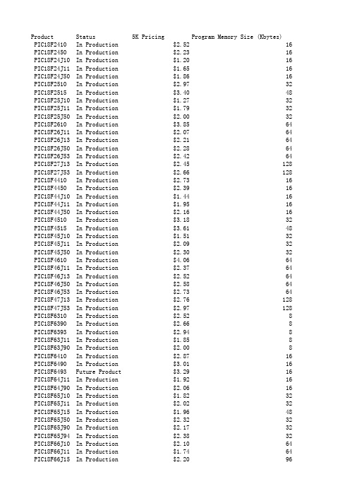
Product Status5K Pricing Program Memory Size (Kbytes)PIC18F2410In Production $2.5216 PIC18F2450In Production $2.2316 PIC18F24J10In Production $1.2016 PIC18F24J11In Production $1.6516 PIC18F24J50In Production $1.8616 PIC18F2510In Production $2.9732 PIC18F2515In Production $3.4048 PIC18F25J10In Production $1.2732 PIC18F25J11In Production $1.7932 PIC18F25J50In Production $2.0032 PIC18F2610In Production $3.8564 PIC18F26J11In Production $2.0764 PIC18F26J13In Production $2.2164 PIC18F26J50In Production $2.2864 PIC18F26J53In Production $2.4264 PIC18F27J13In Production $2.45128 PIC18F27J53In Production $2.66128 PIC18F4410In Production $2.7316 PIC18F4450In Production $2.3916 PIC18F44J10In Production $1.4416 PIC18F44J11In Production $1.9516 PIC18F44J50In Production $2.1616 PIC18F4510In Production $3.1832 PIC18F4515In Production $3.6148 PIC18F45J10In Production $1.5132 PIC18F45J11In Production $2.0932 PIC18F45J50In Production $2.3032 PIC18F4610In Production $4.0664 PIC18F46J11In Production $2.3764 PIC18F46J13In Production $2.5264 PIC18F46J50In Production $2.5864 PIC18F46J53In Production $2.7364 PIC18F47J13In Production $2.76128 PIC18F47J53In Production $2.97128 PIC18F6310In Production $2.528 PIC18F6390In Production $2.668 PIC18F6393In Production $2.948 PIC18F63J11In Production $1.858 PIC18F63J90In Production $2.008 PIC18F6410In Production $2.8716 PIC18F6490In Production $3.0116 PIC18F6493Future Product $3.2916 PIC18F64J11In Production $1.9216 PIC18F64J90In Production $2.0616 PIC18F65J10In Production $1.8232 PIC18F65J11In Production $2.0232 PIC18F65J15In Production $1.9648 PIC18F65J50In Production $2.3232 PIC18F65J90In Production $2.1732 PIC18F65J94In Production $2.3832 PIC18F66J10In Production $2.1064PIC18F66J60In Production $3.0764 PIC18F66J65In Production $3.1996 PIC18F66J90In Production $2.4864 PIC18F66J93In Production $2.6264 PIC18F66J94In Production $2.6964 PIC18F67J10In Production $2.31128 PIC18F67J11In Production $1.95128 PIC18F67J50In Production $2.83128 PIC18F67J60In Production $3.30128 PIC18F67J90In Production $2.72128 PIC18F67J93In Production $2.86128 PIC18F67J94In Production $2.93128 PIC18F8310In Production $3.018 PIC18F8390In Production $3.158 PIC18F8393In Production $3.438 PIC18F83J11In Production $2.118 PIC18F83J90In Production $2.278 PIC18F8410In Production $3.3616 PIC18F8490In Production $3.5016 PIC18F8493In Production $3.7816 PIC18F84J11In Production $2.1816 PIC18F84J90In Production $2.3216 PIC18F85J10In Production $2.0632 PIC18F85J11In Production $2.2832 PIC18F85J15In Production $2.2048 PIC18F85J50In Production $2.5932 PIC18F85J90In Production $2.4432 PIC18F85J94In Production $2.6532 PIC18F86J10In Production $2.3264 PIC18F86J11In Production $2.5964 PIC18F86J15In Production $2.4496 PIC18F86J16In Production $2.7096 PIC18F86J50In Production $2.8664 PIC18F86J55In Production $2.9896 PIC18F86J60In Production $3.3264 PIC18F86J65In Production $3.4496 PIC18F86J72In Production $4.1264 PIC18F86J90In Production $2.7364 PIC18F86J93In Production $2.8864 PIC18F86J94In Production $2.9564 PIC18F87J10In Production $2.55128 PIC18F87J11In Production $2.83128 PIC18F87J50In Production $3.09128 PIC18F87J60In Production $3.56128 PIC18F87J72In Production $4.35128 PIC18F87J90In Production $2.98128 PIC18F87J93In Production $3.12128 PIC18F87J94In Production $3.19128 PIC18F95J94In Production $2.8332PIC18F2525In Production $3.6148 PIC18F2585In Production $4.7748 PIC18F25K80In Production $1.9032 PIC18F2620In Production $4.0664 PIC18F2680In Production $5.0564 PIC18F2682In Production $5.5080 PIC18F2685In Production $5.8796 PIC18F26K20In Production $1.6564 PIC18F26K22In Production $1.9064 PIC18F26K80In Production $2.1864 PIC18F4525In Production $3.8248 PIC18F4585In Production $4.9848 PIC18F45K80In Production $2.1732 PIC18F4620In Production $4.2764 PIC18F4680In Production $5.2664 PIC18F4682In Production $5.7180 PIC18F4685In Production $6.0896 PIC18F46K20In Production $1.8164 PIC18F46K22In Production $2.1664 PIC18F46K80In Production $2.4564 PIC18F6520In Production $5.9332 PIC18F6527In Production $4.6248 PIC18F65K22In Production $2.3932 PIC18F65K80In Production $2.7032 PIC18F65K90In Production $2.5332 PIC18F6622In Production $5.1164 PIC18F6627In Production $6.0296 PIC18F6628In Production $7.1096 PIC18F66K22In Production $2.7064 PIC18F66K80In Production $2.9864 PIC18F66K90In Production $2.8464 PIC18F6722In Production $6.86128 PIC18F6723In Production $7.99128 PIC18F67K22In Production $2.94128 PIC18F67K90In Production $3.08128 PIC18F8520In Production $6.2332 PIC18F8527In Production $5.0448 PIC18F85K22In Production $2.6632 PIC18F85K90In Production $2.8032 PIC18F8622In Production $5.5364 PIC18F8627In Production $6.4496 PIC18F8628In Production $7.5596 PIC18F86K22In Production $2.9764 PIC18F86K90In Production $3.1164 PIC18F8722In Production $7.28128 PIC18F8723In Production $8.44128 PIC18F87K22In Production $3.21128 PIC18F87K90In Production $3.35128 PIC18F1230In Production $2.034PIC18F1320In Production $2.178 PIC18F13K22In Production $1.168 PIC18F13K50In Production $1.328 PIC18F14K22In Production $1.2616 PIC18F14K50In Production $1.5316 PIC18F2220In Production $4.054 PIC18F2221In Production $1.934 PIC18F2320In Production $4.388 PIC18F2321In Production $2.068 PIC18F2331In Production $3.088 PIC18F23K20In Production $1.238 PIC18F23K22In Production $1.318 PIC18F2420In Production $2.7316 PIC18F2423In Production $3.0216 PIC18F2431In Production $3.2216 PIC18F2455In Production $3.3024 PIC18F2458In Production $3.5824 PIC18F2480In Production $3.7216 PIC18F24K20In Production $1.3016 PIC18F24K22In Production $1.4816 PIC18F24K50In Production $1.6516 PIC18F2520In Production $3.1832 PIC18F2523In Production $3.4632 PIC18F2550In Production $3.4432 PIC18F2553In Production $4.1232 PIC18F2580In Production $4.1732 PIC18F25K20In Production $1.3732 PIC18F25K22In Production $1.6232 PIC18F25K50In Production $1.7632 PIC18F4220In Production $4.464 PIC18F4221In Production $2.174 PIC18F4320In Production $4.818 PIC18F4321In Production $2.308 PIC18F4331In Production $3.468 PIC18F43K20In Production $1.468 PIC18F43K22In Production $1.678 PIC18F4420In Production $2.9416 PIC18F4423In Production $3.2316 PIC18F4431In Production $3.6116 PIC18F4455In Production $3.5124 PIC18F4458In Production $3.7924 PIC18F4480In Production $3.9316 PIC18F44K20In Production $1.5316 PIC18F44K22In Production $1.7416 PIC18F4520In Production $3.3932 PIC18F4523In Production $3.6732 PIC18F4550In Production $3.6532 PIC18F4553In Production $4.3332 PIC18F4580In Production $4.3832 PIC18F45K20In Production $1.6032 PIC18F45K22In Production $1.8832 PIC18F45K50In Production $1.9932PIC18F46K40Future Product Call for pricing64 PIC18F47K40Future Product Call for pricing128 PIC18F24K40Future Product Call for pricing16 PIC18F25K40Future Product Call for pricing32 PIC18F45K40Future Product Call for pricing32RAM (bytes)EEPROM / HEF Pin count Max. CPU Speed MHz Peripheral Pin Select (PPS) 76802840No7680 / HEF2848No10240 / HEF2840No38000 / HEF2848Yes38000 / HEF2848Yes153602840No396802840No10240 / HEF2840No38000 / HEF2848Yes38000 / HEF2848Yes396802840No38000 / HEF2848Yes38000 / HEF2848Yes38000 / HEF2848Yes38000 / HEF2848No38000 / HEF2848Yes38000 / HEF2848Yes76804040No7680 / HEF4048No10240 / HEF4040No38000 / HEF4448Yes38000 / HEF4448Yes153604040No396804040No10240 / HEF4040No38000 / HEF4448Yes38000 / HEF4448Yes396804040No38000 / HEF4448Yes38000 / HEF4448Yes38000 / HEF4448Yes38000 / HEF4448Yes38000 / HEF4448Yes38000 / HEF4448Yes76806440No76806440No76806440No10240 / HEF6440No10240 / HEF6440No76806440No76806440No76806432No10240 / HEF6440No10240 / HEF6440No20480 / HEF6440No20480 / HEF6440No20480 / HEF6440No39040 / HEF6448No20480 / HEF6440No38620 / HEF6464No20480 / HEF6440No39040 / HEF6448No 39040 / HEF6448No 39040 / HEF6448No 38080 / HEF6442No 38080 / HEF6442No 39000 / HEF6448No 39000 / HEF6448No 38620 / HEF6464No 39360 / HEF6440No 39040 / HEF6448No 39040 / HEF6448No 38080 / HEF6442No 39000 / HEF6448No 39000 / HEF6448No 38620 / HEF6464No 76808040No 76808040No 76808040No 10240 / HEF8040No 10240 / HEF8040No 76808040No 76808040No 76808032No 10240 / HEF8040No 10240 / HEF8040No 20480 / HEF8040No 20480 / HEF8040No 20480 / HEF8040No 39040 / HEF8048No 20480 / HEF8040No 38620 / HEF8064No 20480 / HEF8040No 39040 / HEF8048No 39360 / HEF8040No 39040 / HEF8048No 39040 / HEF8048No 39040 / HEF8048No 38080 / HEF8042No 38080 / HEF8042No 39230 / HEF8048No 39000 / HEF8048No 39000 / HEF8048No 38620 / HEF8064No 39360 / HEF8040No 39040 / HEF8048No 39040 / HEF8048No 38080 / HEF8042No 39230 / HEF8048No 39000 / HEF8048No 39000 / HEF8048No 38620 / HEF8064No 38620 / HEF10064No38620 / HEF10064No 38080 / HEF10042No 38620 / HEF10064No 396810242840No 332810242840No 364810242864No 396810242840No 332810242840No 332810242840No 332810242840No 393610242864No 389610242864No 364810242864No 396810244040No 332810244040No 364810244464No 396810244040No 332810244040No 332810244040No 332810244040No 393610244064No 389610244064No 364810244464No 204810246440No 393610246440No 204810246464No 364810246464No 204810246464No 393610246440No 393610246440No 393610246440No 386210246464No 364810246464No 382810246464No 393610246440No 393610246440No 386210246464No 382810246464No 204810248040No 393610248040No 204810248064No 204810248064No 393610248040No 393610248040No 393610248040No 386210248064No 382810248064No 393610248040No 393610248040No 386210248064No 409610248064No 256128 / HEF1840No256256 / HEF1840No 256256 / HEF2064No 512256 / HEF2048No 512256 / HEF2064No 768256 / HEF2048No 512256 / HEF2840No 512256 / HEF2840No 512256 / HEF2840No 512256 / HEF2840No 768256 / HEF2840No 512256 / HEF2864No 512256 / HEF2864No 768256 / HEF2840No 768256 / HEF2840No 768256 / HEF2840No 2048256 / HEF2848No 2048256 / HEF2848No 768256 / HEF2840No 768256 / HEF2864No 768256 / HEF2864No 2048256 / HEF2848No 1536256 / HEF2840No 1536256 / HEF2840No 2048256 / HEF2848No 2048256 / HEF2848No 1536256 / HEF2840No 1536256 / HEF2864No 1536256 / HEF2864No 2048256 / HEF2848No 512256 / HEF4040No 512256 / HEF4040No 512256 / HEF4040No 512256 / HEF4040No 768256 / HEF4040No 512256 / HEF4064No 512256 / HEF4064No 768256 / HEF4040No 768256 / HEF4040No 768256 / HEF4040No 2048256 / HEF4048No 2048256 / HEF4048No 768256 / HEF4040No 768256 / HEF4064No 768256 / HEF4064No 1536256 / HEF4040No 1536256 / HEF4040No 2048256 / HEF4048No 2048256 / HEF4048No 1536256 / HEF4040No 1536256 / HEF4064No 1536256 / HEF4064No 20482564048No409610244064Yes 409610244064Yes 10242562864Yes 20482562864Yes 20482564064YesInternal Oscillator# of Comparators Operational Amplifier8 MHz, 32 kHz 20 32 kHz 00 32 kHz 20 8 MHz, 32 kHz 20 8 MHz, 32 kHz 20 8 MHz, 32 kHz 20 8 MHz, 32 kHz 20 32 kHz 20 8 MHz, 32 kHz 20 8 MHz, 32 kHz 20 8 MHz, 32 kHz 20 8 MHz, 32 kHz 20 8 MHz, 32 kHz 30 8 MHz, 32 kHz 20 8 MHz, 32 kHz 30 8 MHz, 32 kHz 30 8 MHz, 32 kHz 30 8 MHz, 32 kHz 20 32 kHz 00 32 kHz 20 8 MHz, 32 kHz 20 8 MHz, 32 kHz 20 8 MHz, 32 kHz 20 8 MHz, 32 kHz 20 32 kHz 20 8 MHz, 32 kHz 20 8 MHz, 32 kHz 20 8 MHz, 32 kHz 20 8 MHz, 32 kHz 20 8 MHz, 32 kHz 30 8 MHz, 32 kHz 20 8 MHz, 32 kHz 30 8 MHz, 32 kHz 30 8 MHz, 32 kHz 30 8 MHz, 32 kHz 20 8 MHz, 32 kHz 20 8 MHz, 32 kHz 20 8 MHz, 32 kHz 20 8 MHz, 32 kHz 20 8 MHz, 32 kHz 20 8 MHz, 32 kHz 20 8 MHz, 32 kHz 20 8 MHz, 32 kHz 20 8 MHz, 32 kHz 20 32 kHz 20 8 MHz, 32 kHz 20 32 kHz 20 8 MHz, 32 kHz 20 8 MHz, 32 kHz 20 8 MHz, 32 kHz 30 32 kHz 20 8 MHz, 32 kHz 208 MHz, 32 kHz 20 8 MHz, 32 kHz 20 32 kHz 20 32 kHz 20 8 MHz, 32 kHz 20 8 MHz, 32 kHz 20 8 MHz, 32 kHz 30 32 kHz 20 8 MHz, 32 kHz 20 8 MHz, 32 kHz 20 32 kHz 20 8 MHz, 32 kHz 20 8 MHz, 32 kHz 20 8 MHz, 32 kHz 30 8 MHz, 32 kHz 20 8 MHz, 32 kHz 20 8 MHz, 32 kHz 20 8 MHz, 32 kHz 20 8 MHz, 32 kHz 20 8 MHz, 32 kHz 20 8 MHz, 32 kHz 20 8 MHz, 32 kHz 20 8 MHz, 32 kHz 20 8 MHz, 32 kHz 20 32 kHz 20 8 MHz, 32 kHz 20 32 kHz 20 8 MHz, 32 kHz 20 8 MHz, 32 kHz 20 8 MHz, 32 kHz 30 32 kHz 20 8 MHz, 32 kHz 20 32 kHz 20 8 MHz, 32 kHz 20 8 MHz, 32 kHz 20 8 MHz, 32 kHz 20 32 kHz 20 32 kHz 20 8 MHz, 32 kHz 20 8 MHz, 32 kHz 20 8 MHz, 32 kHz 20 8 MHz, 32 kHz 30 32 kHz 20 8 MHz, 32 kHz 20 8 MHz, 32 kHz 20 32 kHz 20 8 MHz, 32 kHz 20 8 MHz, 32 kHz 20 8 MHz, 32 kHz 20 8 MHz, 32 kHz 30 8 MHz, 32 kHz 30 32 kHz 2032 kHz 20 8 MHz, 32 kHz 30 8 MHz, 32 kHz 20 8 MHz, 32 kHz 00 16 MHz, 32 kHz 20 8 MHz, 32 kHz 20 8 MHz, 32 kHz 00 8 MHz, 32 kHz 00 8 MHz, 32 kHz 00 16 MHz, 32 kHz 20 16 MHz, 32 kHz 20 16 MHz, 32 kHz 20 8 MHz, 32 kHz 20 8 MHz, 32 kHz 20 16 MHz, 32 kHz 20 8 MHz, 32 kHz 20 8 MHz, 32 kHz 20 8 MHz, 32 kHz 20 8 MHz, 32 kHz 20 16 MHz, 32 kHz 20 16 MHz, 32 kHz 20 16 MHz, 32 kHz 20 None 20 8 MHz, 32 kHz 20 16 MHz, 32 kHz 30 16 MHz, 32 kHz 20 16 MHz, 32 kHz 30 8 MHz, 32 kHz 20 8 MHz, 32 kHz 20 8 MHz, 32 kHz 20 16 MHz, 32 kHz 30 16 MHz, 32 kHz 20 16 MHz, 32 kHz 30 8 MHz, 32 kHz 20 8 MHz, 32 kHz 20 16 MHz, 32 kHz 30 16 MHz, 32 kHz 30 None 20 8 MHz, 32 kHz 20 16 MHz, 32 kHz 30 16 MHz, 32 kHz 30 8 MHz, 32 kHz 20 8 MHz, 32 kHz 20 8 MHz, 32 kHz 20 16 MHz, 32 kHz 30 16 MHz, 32 kHz 30 8 MHz, 32 kHz 20 8 MHz, 32 kHz 20 16 MHz, 32 kHz 30 16 MHz, 32 kHz 30 8 MHz, 32 kHz 30 8 MHz, 32 kHz 3016 MHz, 32 kHz 20 16 MHz, 32 kHz 20 16 MHz, 32 kHz 20 16 MHz, 32 kHz 20 8 MHz, 32 kHz 20 8 MHz, 32 kHz 20 8 MHz, 32 kHz 20 8 MHz, 32 kHz 20 8 MHz, 32 kHz 00 16 MHz, 32 kHz 20 16 MHz, 32 kHz 20 8 MHz, 32 kHz 20 8 MHz, 32 kHz 20 8 MHz, 32 kHz 00 8 MHz, 32 kHz 20 8 MHz, 32 kHz 20 8 MHz, 32 kHz 00 16 MHz, 32 kHz 20 16 MHz, 32 kHz 20 16 MHz, 32 kHz 20 8 MHz, 32 kHz 20 8 MHz, 32 kHz 20 8 MHz, 32 kHz 20 8 MHz, 32 kHz 20 8 MHz, 32 kHz 00 16 MHz, 32 kHz 20 16 MHz, 32 kHz 20 16 MHz 20 8 MHz, 32 kHz 20 8 MHz, 32 kHz 20 8 MHz, 32 kHz 20 8 MHz, 32 kHz 20 8 MHz, 32 kHz 00 16 MHz, 32 kHz 20 16 MHz, 32 kHz 20 8 MHz, 32 kHz 20 8 MHz, 32 kHz 20 8 MHz, 32 kHz 00 8 MHz, 32 kHz 20 8 MHz, 32 kHz 20 8 MHz, 32 kHz 20 16 MHz, 32 kHz 20 16 MHz, 32 kHz 20 8 MHz, 32 kHz 20 8 MHz, 32 kHz 20 8 MHz, 32 kHz 20 8 MHz, 32 kHz 20 8 MHz, 32 kHz 20 16 MHz, 32 kHz 20 16 MHz, 32 kHz 20 16 MHz 20 64MHZ, 64KHz 2064MHZ, 64KHz 20 64MHZ, 64KHz 20 64MHZ, 64KHz 20 64MHZ, 64KHz 20 64MHZ, 64KHz 20Total # of A/D channels Max A/D Resolution (bits)Number of D/A Converters101001010010100101001010010100101001010010100101001010010100101201010013120101201012013100131001310013100131001310013100131001310013100131001310013120131001312013120131201210012100121201210012100121001210012120121001210011100121001110081001210016120111001110011100 8100 8100 11100 11100 12100 12120 16120 11100 11100 8100 11100 12100 12120 16120 12100 12100 12120 12100 12100 12100 12100 12120 12100 12100 15100 12100 15100 12100 12100 24120 15100 12100 15100 12100 12100 12100 15100 15100 2160 12100 12120 24120 15100 12100 12100 15100 2160 12100 12120 24120 24120 1610024120 16100 24120 10100 8100 8120 10100 8100 8100 8100 10100 17101 8120 13100 11100 11120 13100 11100 11100 11100 13100 28101 11120 12100 12100 16120 11120 16120 12100 12100 12120 16120 11120 16120 12100 12120 16120 16120 16100 16100 24120 24120 16100 16100 16120 24120 24120 16100 16120 24120 24120 4100 41007100 12100 9100 12100 9100 10100 10100 10100 10100 5100 10100 17101 10100 10120 5100 10100 10120 8100 10100 17101 14101 10100 10120 10100 10120 8100 10100 17101 14101 13100 13100 13100 13100 9100 13100 28101 13100 13120 9100 13100 13120 11100 13100 28101 13100 13120 13100 13120 11100 13100 28101 25101 2410135101 35101 24101 24101 35101Max D/A Resolution (bits)Internal Voltage Reference (Bandgap)Zero Cross detect0No No0No No0No No0No No0No No0No No0No No0No No0No No0No No0No No0No No0No No0No No0No No0No No0No No0No No0No No0No No0No No0No No0No No0No No0No No0No No0No No0No No0No No0No No0No No0No No0No No0No No0No No0No No0No No0No No0No No0No No0No No0No No0No No0No No0No No0No No0No No0No No0No No0Yes No0No No0No No 0No No 0No No 0No No 0No No 0No No 0No No 0Yes No 0No No 0No No 0No No 0No No 0No No 0No No 0Yes No 0No No 0No No 0No No 0No No 0No No 0No No 0No No 0No No 0No No 0No No 0No No 0No No 0No No 0No No 0No No 0Yes No 0No No 0No No 0No No 0No No 0No No 0No No 0No No 0No No 0No No 0No No 0No No 0Yes No 0No No 0No No 0No No 0No No 0No No 0No No 0No No 0Yes No 0No No0Yes No 0No No 0Yes No 0No No 0No No 0No No 0No No 0No No 0No No 0No No 0Yes No 5Yes No 0No No 0No No 0No No 0No No 0No No 0No No 0No No 0No No 0Yes No 5Yes No 0No No 0No No 0No No 0Yes No 0No No 0Yes No 0No No 0No No 0No No 0Yes No 0No No 0Yes No 0No No 0No No 0Yes No 0Yes No 0No No 0No No 0Yes No 0Yes No 0No No 0No No 0No No 0Yes No 0Yes No 0No No 0No No 0Yes No 0Yes No 0No No0No No 0Yes No 0Yes No 0Yes No 0Yes No 0No No 0No No 0No No 0No No 0No No 0Yes No 5Yes No 0No No 0No No 0No No 0No No 0No No 0No No 0Yes No 5Yes No 5Yes No 0No No 0No No 0No No 0No No 0No No 0Yes No 5Yes No 5Yes No 0No No 0No No 0No No 0No No 0No No 0Yes No 5No No 0No No 0No No 0No No 0No No 0No No 0No No 0Yes No 5Yes No 0No No 0No No 0No No 0No No 0No No 0Yes No 5Yes No 5Yes No5Yes Yes 5Yes Yes 5Yes Yes 5Yes Yes 5Yes YesSlope Compensation / Programmable Ramp Generator Data Signal Modulator (DSM)0 00 0 0 0 0 0 0 0 0 0 0 0 0 0 0 0 0 0 0 0 0 0 0 0 0 0 0 0 0 0 0 0 0 0 0 0 0 0 0 0 0 0 0 0 0 0 0 00 000 00 00 00 00Max 8 Bit Digital Timers Max 16 Bit Digital Timers Signal Measurement Timer131212232313131223231323442344444413121223231313122323132344234444441313131313131313131323132323130402323231313040 232323231331040 13131313132313131313231323231304232323232323232331131304232323233113130404130 130 230 130 130 130 130 130 340 230 130 130 230 130 130 130 130 130 340 230 230 230 440 230 440 230 230 230 650 230 650 230 230 650 650 230 230 440 440 230 230 230 650 650 230 230 650 650 0213 13 13 13 13 13 13 13 13 13 13 13 13 13 13 13 13 22 13 13 13 13 13 13 34 22 13 13 13 13 13 13 13 13 13 13 13 13 13 13 13 13 13 13 13 13 13 34 22430 430 430 430 430Hardware Limit Timer Max # PWM outputs (including complementary outputs)000 000 0000 00 00 00 00 00 00 00 00 00 00 00 00 00 00 00 00 00 00 00 00 00 00 00 00 00 00 00 00 00 00 00 00 00 00 00 00 00 00 00 00 00 00 00 00 00 00 000 0 0 0 0 0 0 0 0 0 0 0 0 0 0 0 0 0 0 0 0 0 0 0 0 0 0 0 0 0 0 0 0 0 0 0 0 0 0 0 0 0 0 0 0 0 0 0 010 10 10 10 10Max PWM Resolution (bits)Angular Timer Math Accelerator ADC Math Pak UART10110110110210210110110110210210110210210210210210210110110110210210110110110210210110210210210210210210210210210210210210210210210210210210210210204102101 101 102 102 04 102 102 102 101 102 102 04 102 102 102 102 102 102 102 102 102 102 102 102 102 102 102 04 102 102 102 102 102 102 102 102 102 102 102 04 102 102 102 102 102 102 102 04 0410No No No1 10No No No1 10No No No2 10No No No1 10No No No1 10No No No1 10No No No1 10No No No1 0No No No2 10No No No2 10No No No1 10No No No1 10No No No2 10No No No1 10No No No1 10No No No1 10No No No1 10No No No1 0No No No2 10No No No2 10No No No2 10No No No2 0No No No2 10No No No2 0No No No2 10No No No2 10No No No2 10No No No2 0No No No2 10No No No2 0No No No2 10No No No2 10No No No2 0No No No2 0No No No2 10No No No2 10No No No2 0No No No2 0No No No2 10No No No2 10No No No2 10No No No2 0No No No2 0No No No2 10No No No2 10No No No2 0No No No2 0No No No2 01101 101 101 101 101 101 101 101 02 101 101 101 101 101 101 101 02 101 101 101 101 101 101 101 102 101 101 101 101 101 101 101 02 101 101 101 101 101 101 101 02 101 101 101 101 101 101 102 10110No No No1 10No No No1 10No No No1 10No No No1 10No No No1SPI鈩?,I2C"Number of USB Modules Windowed Watchdog Timer (WWDT)CRC/Scan 110No001No110No220No221No110No110No110No220No221No110No220No220No221No221No220No221No110No001No220No220No221No110No110No220No220No221No110No220No220No221No221No220No221No110No110No110No110No110No110No110No110No110No110No220No110No220No221No110No221No220No220No 221No 221No 110No 110No 110No 110No 221No 220No 220No 221No 110No 110No 110No 221No 110No 110No 110No 110No 110No 110No 110No 110No 110No 110No 220No 110No 220No 221No 110No 221No 220No 220No 220No 220No 221No 221No 110No 110No 110No 110No 110No 221No 220No 220No 221No 110No 110No 110No 110No 221No 221No221No 220No 221No 110No 110No 110No 110No 110No 110No 110No 110No 220No 110No 110No 110No 110No 110No 110No 110No 110No 110No 220No 110No 110No 220No 220No 110No 220No 220No 220No 220No 220No 110No 220No 220No 220No 220No 220No 110No 220No 220No 220No 220No 220No 220No 220No 220No 220No 220No 220No 220No 000No000No 110No 111No 110No 111No 110No 110No 110No 110No 110No 110No 220No 110No 110No 110No 111No 111No 110No 110No 220No 111No 110No 110No 111No 111No 110No 110No 220No 111No 110No 110No 110No 110No 110No 110No 220No 110No 110No 110No 111No 111No 110No 110No 220No 110No 110No 111No 111No 110No 110No 220No 111No110Yes 110Yes 110Yes 110Yes 110Yes。
PIC18F1XK22_LF1XK22 Family Silicon Errata and Data Sheet Clarification

© 2009 Microchip Technology Inc.DS80437B-page 1PIC18F1XK22/LF1XK22The PIC18F1XK22/LF1XK22 family devices that you have received conform functionally to the current Device Data Sheet (DS41365B ), except for the anomalies described in this document.The silicon issues discussed in the following pages are for silicon revisions with the Device and Revision IDs listed in Table 1. The silicon issues are summarized in T able 2.The errata described in this document will be addressed in future revisions of the PIC18F1XK22/LF1XK22silicon.Data Sheet clarifications and corrections start on page 6,following the discussion of silicon issues.The silicon revision level can be identified using the current version of MPLAB ® IDE and Microchip’s programmers, debuggers, and emulation tools, which are available at the Microchip corporate web site ().For example, to identify the silicon revision level using MPLAB IDE in conjunction with MPLAB ICD 2 or PICkit™ 3:1.Using the appropriate interface, connect the device to the MPLAB ICD 2 programmer/debugger or PICkit™ 3.2.From the main menu in MPLAB IDE, select Configure>Select Device , and then select the target part number in the dialog box.3.Select the MPLAB hardware tool (Debugger>Select Tool ).4.Perform a “Connect” operation to the device (Debugger>Connect ). Depending on the development tool used, the part number and Device Revision ID value appear in the Output window.The DEVREV values for the various PIC18F1XK22/LF1XK22 silicon revisions are shown in Table 1.Note:This document summarizes all silicon errata issues from all revisions of silicon,previous as well as current.Note:If you are unable to extract the silicon revision level, please contact your local Microchip sales office for assistance.TABLE 1:SILICON DEVREV VALUESPart NumberDevice ID Revision ID for Silicon Revision (1)A1A2A3PIC18F14K224F20h 01h 02h 03h PIC18F13K224F40h 01h 02h 03h PIC18LF14K224F60h 01h 02h 03h PIC18LF13K224F80h01h02h03hNote 1:The Device IDs (DEVID and DEVREV) are located at the last two implemented addresses in program memory. They are shown in hexadecimal in the format “DEVID:DEVREF”.2:Refer to the “PIC18F1XK22/LF1XK22 Flash Memory Programming Specification” (DS41357) for detailed information on Device and Revision IDs for your specific device.PIC18F1XK22/LF1XK22 Family Silicon Errata and Data Sheet ClarificationPIC18F1XK22/LF1XK22DS80437B-page 2© 2009 Microchip Technology Inc.TABLE 2:SILICON ISSUE SUMMARYSilicon Errata Issues1.Module:ADC (Analog-to-DigitalConverter)ADC conversion on AN3/OSC2 will have large INL error up to approximately 8LSb.Work aroundNone for the AN3 pin. For better accuracy, use another analog pin.Affected Silicon Revisions 2.Module:ECCP2.1Changing direction in Full-Bridge mode inserts a dead band time of 4/F OSC *TMR2prescale instead of 1/F OSC *TMR2 prescale as specified in the data sheet.Work around None.Affected Silicon Revisions 2.2In Full-Bridge mode, when PR2=CCPR1L,DC1B<1:0> = 00, and the direction is changed, then the dead time before the modulated output starts is compromised.The modulated signal improperly starts immediately with the direction change and stays on for T OSC *TMR2Presale *DC1B<1:0>.Work aroundAvoid changing direction when the duty cycle is within three least significant steps of 100% duty cycle. Instead, clear the DC1B<1:0> bits before the direction change and then set them to the desired value after the direction change is complete.Affected Silicon Revisions 3.Module:EUSART3.1In Asynchronous Receive mode, the RCIDL bit of the BAUDCON register will properly go low when a low pulse greater than 1/16th of a bit time is received on the RX input. The RCIDL bit will then improperly go high if a low pulse less than 1/16 bit time occurs on the RX input within one bit period after the falling edge of the first pulse. This erratum affects only users monitoring the RCIDL bit as a part of their serial protocol.Module Feature Item Number Issue SummaryAffected Revisions (1)A1A2A3ADC ADC Conversion rge INL error on AN3.X X X ECCP Full Bridge mode2.Delay time with direction change.X X X EUSART — 3.RCIDL bit, clearing the OERR flag, and RX pin.X X X MSSP —4.I 2C™ mode and SPI mode.X XXOscillator LP Osc. 5.Osc. switching and LP Osc. fails at hot.X V REF CV REF output6.RC2 disabled.X ICSP™—7.ICSP works only at V DD >2V.X X X Internal Oscillator —8.Frequency tolerance.XXXNote 1:Only those issues indicated in the last column apply to the current silicon revision.Note:This document summarizes all silicon errata issues from all revisions of silicon,previous as well as current. Only the issues indicated by the shaded column in the following tables apply to the current silicon revision (A1).A1A2A3XXXA1A2A3XXXA1A2A3XXXPIC18F1XK22/LF1XK22Work aroundNone.Affected Silicon Revisions3.2The OERR flag of the RCSTA register isreset only by either clearing the CREN bit ofthe RCSTA register or by a device Reset.Clearing the SPEN bit of the RCSTA registerdoes not clear the OERR flag.Work aroundClear the OERR flag by clearing the CRENbit in lieu of clearing the SPEN bit.Affected Silicon Revisions3.3When the SPEN bit of the RCSTA register isset and the CREN bit of the RCSTA registeris clear, the RX pin is not available for gen-eral purpose output. Likewise, when theSPEN bit of the RCSTA register is set andthe TXEN bit of the TXSTA register is clear,the TX pin is not available for general pur-pose output. However, both the RX and TXpins can be read regardless of the state ofthe RCSTA and TXSTA control registers.Work aroundNone.Affected Silicon Revisions4.Module:MSSP (Master SynchronousSerial Port)4.1In I2C™ Master mode, baud rates obtainedby setting SSPADD to a value less than 0x03will cause unexpected operation.Work aroundEnsure SSPADD is set to a value greaterthan or equal to 0x03.Affected Silicon Revisions 4.2In SPI Master mode, when the CKE bit iscleared and the SMP bit is set, the last bit ofthe incoming data stream (bit 0) at the SDIpin will not be sampled properly.Work aroundNone.Affected Silicon Revisions4.3When SPI is enabled in Master mode withCKE=1 and CKP=0, a 1/F OSC wide pulsewill occur on the SCK pin.Work aroundConfigure the SCK pin as an input until afterthe MSSP is setup.Affected Silicon Revisions4.4I2C Master mode, SSPADD values of 0x00,0x01, 0x02 are invalid. The current I2C BaudRate Generator (BSG) is not set up togenerate a clock signal for these values.Work aroundNone.Affected Silicon Revisions4.5I2C Master mode, RCEN bit not cleared byhardware if improper Stop is received on thebus.Work aroundReset the module via clearing and settingthe SSPEN bit of SSPCON1.Affected Silicon RevisionsA1A2A3 X X XA1A2A3 X X XA1A2A3 X X XA1A2A3 X X X A1A2A3 X X XA1A2A3 X X XA1A2A3 X X XA1A2A3 X X X© 2009 Microchip Technology Inc.DS80437B-page 3PIC18F1XK22/LF1XK22DS80437B-page 4© 2009 Microchip Technology Inc.4.6SPI Master mode, when the SPI clock is configured for Timer2/2(SSPCON1<3:0>=0011), the first SPI high time may be short.Work around None.Option 1: Ensure TMR2 value rolls over tozero immediately before writing to SSPBUF.Option 2: Turn Timer2 off and clear TMR2before writing SSPBUF. Enable TMR2 after SSPBUF is written.Affected Silicon Revisions 4.7In any SPI Master mode, SCK =TMR2/2; if SSPBUF is written to while shifting out data,a ninth SCK pulse is incorrectly generated.At that point, the module locks user from writ-ing to the SSPBUF register, but a write attempt will still cause 8 or 9 more SCK pulses to be generated.Work aroundThe WCOL bit of the SSPCON register is correctly set to indicate that there was a write collision. Any time this bit is set the module must be disabled and enabled (toggle SSPEN) to return to correct operation. The bus will remain out of synchronization.Affected Silicon Revisions .5.Module:Oscillator5.1Disabling the Primary External Oscillator circuitry (PRI_SD = 1) immediately following a change in system clock from external LP oscillator to the internal oscillator will halt code execution indefinitely.Work aroundAfter changing from external LP oscillator to the internal oscillator, allow at least two instruction cycles before disabling the Primary External Oscillator circuitry.Affected Silicon Revisions 5.2The external LP Oscillator could fail operation at temperatures above 100degrees Celsius.Work around None.Affected Silicon Revisions 6.Module:Programmable VoltageReferenceThe V REF voltage reference can be output to the device CV REF pin by setting the DAC1OE bit of the VREFCON1 register to ‘1’. When the CV REF pin is enabled, pin RC2 is incorrectly set to Analog mode. The digital output buffer and digital input threshold detector functions of that pin are disabled.Work aroundPin RC2 may only be used for analog functions when the voltage reference output is enabled on the CV REF pin. Ensure that the TRIS bit for pin RA0 is set to ‘1’ for proper operation of the CV REF output.Affected Silicon Revisions 7.Module:In-Circuit Serial Programming™(ICSP™)The device cannot be programmed using ICSP when the device V DD is less than 2.0 volts.Work aroundEnsure that the device voltage is 2.0 volts or higher when programming the device.Affected Silicon Revisions A1A2A3X XXA1A2A3XXXA1A2A3XA1A2A3XA1A2A3XA1A2A3XXXPIC18F1XK22/LF1XK228.Module: Internal OscillatorThe frequency tolerance of the HFINTOSC inter-nal oscillator is +2% to -2.5% from 0-85°C.Work aroundNone.Affected Silicon RevisionsA1A2A3X X X© 2009 Microchip Technology Inc.DS80437B-page 5PIC18F1XK22/LF1XK22DS80437B-page 6© 2009 Microchip Technology Inc.Data Sheet ClarificationsThe following typographic corrections and clarifications are to be noted for the latest version of the device data sheet (DS41365B ).1.Module: Electrical SpecificationsIn Table 25-10 Comparator Specifications of the data sheet (DS41365B ), the Input Offset Voltage should be +/-50mV in High-Power mode and +/-80mV in Low-Power mode as shown below.TABLE 25-10:COMPARATOR SPECIFICATIONS2.Module:Device OverviewIn Table 1-2, PIC18F1XK22/LF1XK22 Pin Sum-mary of the data sheet (DS41365B ), under pin name RA2, the Buffer Type should be ‘ST ’.Note:Corrections are shown in bold . Where possible, the original bold text formatting has been removed for clarity.Operating Conditions: 1.8V < V DD < 5.5V, -40°C < T A < +125°C (unless otherwise stated).Param No.Sym.CharacteristicsMin.Typ. Max.UnitsComments CM01V IOFF Input Offset Voltage—±7.5±50 mV High-Power mode ——±80 mV Low-Power modeCM02V ICM Input Common Mode Voltage 0—V DD V CM03CMRR Common Mode Rejection Ratio 55——dB CM04T RESP Response Time—150400ns Note 1CM05T MC 2OVComparator Mode Change to Output Valid*——10μs*These parameters are characterized but not tested.Note 1:Response time measured with one comparator input at V DD /2, while the other input transitions from V SS to V DD .PIC18F1XK22/LF1XK22 APPENDIX A:DOCUMENTREVISION HISTORYRev. A Document (3/2009)Initial release of this document.Rev. B Document (5/2009)Revised Table 1; Added Table 2; Added Module 8:Internal Oscillator.Added Data Sheet Clarifications Module 1: ElectricalSpecifications and Module 2: Device Overview.© 2009 Microchip Technology Inc.DS80437B-page 7PIC18F1XK22/LF1XK22NOTES:DS80437B-page 8© 2009 Microchip Technology Inc.© 2009 Microchip Technology Inc.DS80437B-page 9Information contained in this publication regarding device applications and the like is provided only for your convenience and may be superseded by updates. It is your responsibility to ensure that your application meets with your specifications.MICROCHIP MAKES NO REPRESENTATIONS OR WARRANTIES OF ANY KIND WHETHER EXPRESS OR IMPLIED, WRITTEN OR ORAL, STATUTORY OR OTHERWISE, RELATED TO THE INFORMATION,INCLUDING BUT NOT LIMITED TO ITS CONDITION,QUALITY , PERFORMANCE, MERCHANTABILITY OR FITNESS FOR PURPOSE . Microchip disclaims all liability arising from this information and its use. Use of Microchip devices in life support and/or safety applications is entirely at the buyer’s risk, and the buyer agrees to defend, indemnify and hold harmless Microchip from any and all damages, claims,suits, or expenses resulting from such use. No licenses are conveyed, implicitly or otherwise, under any Microchip intellectual property rights.TrademarksThe Microchip name and logo, the Microchip logo, dsPIC, K EE L OQ , K EE L OQ logo, MPLAB, PIC, PICmicro, PICSTART, rfPIC and UNI/O are registered trademarks of Microchip Technology Incorporated in the U.S.A. and other countries.FilterLab, Hampshire, HI-TECH C, Linear Active Thermistor, MXDEV , MXLAB, SEEVAL and The Embedded Control Solutions Company are registered trademarks of Microchip Technology Incorporated in the U.S.A.Analog-for-the-Digital Age, Application Maestro, CodeGuard, dsPICDEM, , dsPICworks, dsSPEAK, ECAN, ECONOMONITOR, FanSense, HI-TIDE, In-Circuit Serial Programming, ICSP , ICEPIC, Mindi, MiWi, MPASM, MPLAB Certified logo, MPLIB, MPLINK, mTouch, nanoWatt XLP , Omniscient Code Generation, PICC, PICC-18, PICkit,PICDEM, , PICtail, PIC 32 logo, REAL ICE, rfLAB, Select Mode, Total Endurance, TSHARC, WiperLock and ZENA are trademarks of Microchip Technology Incorporated in the U.S.A. and other countries.SQTP is a service mark of Microchip Technology Incorporated in the U.S.A.All other trademarks mentioned herein are property of their respective companies.© 2009, Microchip Technology Incorporated, Printed in the U.S.A., All Rights Reserved.Printed on recycled paper.Note the following details of the code protection feature on Microchip devices:•Microchip products meet the specification contained in their particular Microchip Data Sheet.•Microchip believes that its family of products is one of the most secure families of its kind on the market today, when used in the intended manner and under normal conditions.•There are dishonest and possibly illegal methods used to breach the code protection feature. All of these methods, to ourknowledge, require using the Microchip products in a manner outside the operating specifications contained in Microchip’s Data Sheets. Most likely, the person doing so is engaged in theft of intellectual property.•Microchip is willing to work with the customer who is concerned about the integrity of their code.•Neither Microchip nor any other semiconductor manufacturer can guarantee the security of their code. Code protection does not mean that we are guaranteeing the product as “unbreakable.”Code protection is constantly evolving. We at Microchip are committed to continuously improving the code protection features of our products. Attempts to break Microchip’s code protection feature may be a violation of the Digital Millennium Copyright Act. If such acts allow unauthorized access to your software or other copyrighted work, you may have a right to sue for relief under that Act.Microchip received ISO/TS-16949:2002 certification for its worldwide headquarters, design and wafer fabrication facilities in Chandler and Tempe, Arizona; Gresham, Oregon and design centers in California and India. The Company’s quality system processes and procedures are for its PIC ® MCUs and dsPIC ® DSCs, K EE L OQ ® code hoppingdevices, Serial EEPROMs, microperipherals, nonvolatile memory and analog products. In addition, Microchip’s quality system for the design and manufacture of development systems is ISO 9001:2000 certified.AMERICASCorporate Office2355 West Chandler Blvd. Chandler, AZ 85224-6199 Tel: 480-792-7200Fax: 480-792-7277 Technical Support: Web Address: AtlantaDuluth, GATel: 678-957-9614Fax: 678-957-1455BostonWestborough, MATel: 774-760-0087Fax: 774-760-0088 ChicagoItasca, ILTel: 630-285-0071Fax: 630-285-0075 Cleveland Independence, OHTel: 216-447-0464Fax: 216-447-0643DallasAddison, TXTel: 972-818-7423Fax: 972-818-2924DetroitFarmington Hills, MITel: 248-538-2250Fax: 248-538-2260 KokomoKokomo, INTel: 765-864-8360Fax: 765-864-8387Los AngelesMission Viejo, CATel: 949-462-9523Fax: 949-462-9608Santa ClaraSanta Clara, CATel: 408-961-6444Fax: 408-961-6445 TorontoMississauga, Ontario, CanadaTel: 905-673-0699Fax: 905-673-6509ASIA/PACIFICAsia Pacific OfficeSuites 3707-14, 37th FloorTower 6, The GatewayHarbour City, KowloonHong KongTel: 852-2401-1200Fax: 852-2401-3431Australia - SydneyTel: 61-2-9868-6733Fax: 61-2-9868-6755China - BeijingTel: 86-10-8528-2100Fax: 86-10-8528-2104China - ChengduTel: 86-28-8665-5511Fax: 86-28-8665-7889China - Hong Kong SARTel: 852-2401-1200Fax: 852-2401-3431China - NanjingTel: 86-25-8473-2460Fax: 86-25-8473-2470China - QingdaoTel: 86-532-8502-7355Fax: 86-532-8502-7205China - ShanghaiTel: 86-21-5407-5533Fax: 86-21-5407-5066China - ShenyangTel: 86-24-2334-2829Fax: 86-24-2334-2393China - ShenzhenTel: 86-755-8203-2660Fax: 86-755-8203-1760China - WuhanTel: 86-27-5980-5300Fax: 86-27-5980-5118China - XiamenTel: 86-592-2388138Fax: 86-592-2388130China - XianTel: 86-29-8833-7252Fax: 86-29-8833-7256China - ZhuhaiTel: 86-756-3210040Fax: 86-756-3210049ASIA/PACIFICIndia - BangaloreTel: 91-80-3090-4444Fax: 91-80-3090-4080India - New DelhiTel: 91-11-4160-8631Fax: 91-11-4160-8632India - PuneTel: 91-20-2566-1512Fax: 91-20-2566-1513Japan - YokohamaTel: 81-45-471- 6166Fax: 81-45-471-6122Korea - DaeguTel: 82-53-744-4301Fax: 82-53-744-4302Korea - SeoulTel: 82-2-554-7200Fax: 82-2-558-5932 or82-2-558-5934Malaysia - Kuala LumpurTel: 60-3-6201-9857Fax: 60-3-6201-9859Malaysia - PenangTel: 60-4-227-8870Fax: 60-4-227-4068Philippines - ManilaTel: 63-2-634-9065Fax: 63-2-634-9069SingaporeTel: 65-6334-8870Fax: 65-6334-8850Taiwan - Hsin ChuTel: 886-3-6578-300Fax: 886-3-6578-370Taiwan - KaohsiungTel: 886-7-536-4818Fax: 886-7-536-4803Taiwan - TaipeiTel: 886-2-2500-6610Fax: 886-2-2508-0102Thailand - BangkokTel: 66-2-694-1351Fax: 66-2-694-1350EUROPEAustria - WelsTel: 43-7242-2244-39Fax: 43-7242-2244-393Denmark - CopenhagenTel: 45-4450-2828Fax: 45-4485-2829France - ParisTel: 33-1-69-53-63-20Fax: 33-1-69-30-90-79Germany - MunichTel: 49-89-627-144-0Fax: 49-89-627-144-44Italy - MilanTel: 39-0331-742611Fax: 39-0331-466781Netherlands - DrunenTel: 31-416-690399Fax: 31-416-690340Spain - MadridTel: 34-91-708-08-90Fax: 34-91-708-08-91UK - WokinghamTel: 44-118-921-5869Fax: 44-118-921-5820 W ORLDWIDE S ALES AND S ERVICE03/26/09DS80437B-page 10© 2009 Microchip Technology Inc.。
关于头文件的进一步理解基于PIC单片机

关于头文件的进一步理解基于PIC单片机一:关于处理器的寄存器定义针对处理器的寄存器定义文件是一个汇编文件,包含特定器件上所有特殊功能寄存器的定义。
编译时,针对处理器的寄存器定义文件将被编译成需要链接到应用程序的目标文件。
例如,在PIC18C452 针对处理器的寄存器定义文件中,PORTA 定义为:SFR_UNBANKED0 UDATA_ACS Hf80PORTAPORTAbits RES 1 ; 0xf80 第一行指定PORTA 所在的数据寄存器存储区和这个存储区的起始地址。
PORTA有两个标号,PORTAbits 和PORTA,都指向同一个地址(本例中是0xf80)。
二:关于头文件声明针对处理器的头文件是包含特殊功能寄存器外部声明的C 文件,特殊功能寄存器在寄存器定义文件中定义。
例如,在PIC18C452 的针对处理器头文件中,PORTA 声明为:extern volatile near unsigned char PORTA;和:extern volatile near union { struct { unsigned RA0:1; unsigned RA1:1; unsigned RA2:1; unsigned RA3:1; unsigned RA4:1; unsigned RA5:1; unsigned RA6:1; } ; struct { unsigned AN0:1; unsigned AN1:1; unsigned AN2:1; unsigned AN3:1; unsigned T0CKI:1; unsigned SS:1; unsigned OSC2:1; } ; struct { unsigned :2;//填充前两位unsigned VREFM:1; unsigned VREFP:1; unsigned :1;//此位被填充unsigned AN4:1; unsigned CLKOUT:1; } ; struct { unsigned :5;//填充前五位unsigned LVDIN:1; } ;} PORTAbits ;第一个声明指定PORTA 是一个字节(unsigned char)。
- 1、下载文档前请自行甄别文档内容的完整性,平台不提供额外的编辑、内容补充、找答案等附加服务。
- 2、"仅部分预览"的文档,不可在线预览部分如存在完整性等问题,可反馈申请退款(可完整预览的文档不适用该条件!)。
- 3、如文档侵犯您的权益,请联系客服反馈,我们会尽快为您处理(人工客服工作时间:9:00-18:30)。
* RB3 is the alternate pin for the CCP2 pin multiplexing. Note: Pin compatible with 40-pin PIC16C7X devices.
Analog Features:
• Compatible 10-bit Analog-to-Digital Converter module (A/D) with: - Fast sampling rate - Conversion available during SLEEP - DNL = ±1 LSb, INL = ±1 LSb • Programmable Low Voltage Detection (LVD) module - Supports interrupt-on-low voltage detection • Programmable Brown-out Reset (BOR)
On-Chip Program Memory Device EPROM (bytes) 16K 32K 16K 32K # Single Word Instructions 8192 16384 8192 16384 On-Chip RAM (bytes) 512 1536 512 1536
Pin Diagrams
Microchip received QS-9000 quality system certification for its worldwide headquarters, design and wafer fabrication facilities in Chandler and Tempe, Arizona in July 1999. The Company’s quality system processes and procedures are QS-9000 compliant for its PICmicro® 8-bit MCUs, KEELOQ® code hopping devices, Serial EEPROMs and microperipheral products. In addition, Microchip’s quality system for the design and manufacture of development systems is ISO 9001 certified.
DS39026C - page ii
2001 Microchip Technology Inc.
芯天下--/
PIC18CXX2
High Performance Microcontrollers with 10-bit A/D
High Performance RISC CPU:
Peripheral Features:
• High current sink/source 25 mA/25 mA • Three external interrupt pins • Timer0 module: 8-bit/16-bit timer/counter with 8-bit programmable prescaler • Timer1 module: 16-bit timer/counter • Timer2 module: 8-bit timer/counter with 8-bit period register (time-base for PWM) • Timer3 module: 16-bit timer/counter • Secondary oscillator clock option - Timer1/Timer3 • Two Capture/Compare/PWM (CCP) modules. CCP pins that can be configured as: - Capture input: capture is 16-bit, max. resolution 6.25 ns (TCY/16) - Compare is 16-bit, max. resolution 100 ns (TCY) - PWM output: PWM resolution is 1- to 10-bit. Max. PWM freq. @: 8-bit resolution = 156 kHz 10-bit resolution = 39 kHz • Master Synchronous Serial Port (MSSP) module. Two modes of operation: - 3-wire SPI™ (பைடு நூலகம்upports all 4 SPI modes) - I2C™ master and slave mode • Addressable USART module: - Supports interrupt on Address bit • Parallel Slave Port (PSP) module
• C compiler optimized architecture/instruction set - Source code compatible with the PIC16CXX instruction set • Linear program memory addressing to 2 Mbytes • Linear data memory addressing to 4 Kbytes
PIC18C242 PIC18C252 PIC18C442 PIC18C452
• Up to 10 MIPs operation: - DC - 40 MHz osc./clock input - 4 MHz - 10 MHz osc./clock input with PLL active • 16-bit wide instructions, 8-bit wide data path • Priority levels for interrupts • 8 x 8 Single Cycle Hardware Multiplier
DIP, Windowed CERDIP
MCLR/VPP RA0/AN0 RA1/AN1 RA2/AN2/VREFRA3/AN3/VREF+ RA4/T0CKI RA5/AN4/SS/LVDIN RE0/RD/AN5 RE1/WR/AN6 RE2/CS/AN7 VDD VSS OSC1/CLKI OSC2/CLKO/RA6 RC0/T1OSO/T1CKI RC1/T1OSI/CCP2* RC2/CCP1 RC3/SCK/SCL RD0/PSP0 RD1/PSP1 1 2 3 4 5 6 7 8 9 10 11 12 13 14 15 16 17 18 19 20 40 39 38 37 36 35 34 33 32 31 30 29 28 27 26 25 24 23 22 21 RB7 RB6 RB5 RB4 RB3/CCP2* RB2/INT2 RB1/INT1 RB0/INT0 VDD VSS RD7/PSP7 RD6/PSP6 RD5/PSP5 RD4/PSP4 RC7/RX/DT RC6/TX/CK RC5/SDO RC4/SDI/SDA RD3/PSP3 RD2/PSP2
Trademarks The Microchip name, logo, PIC, PICmicro, PICMASTER, PICSTART, PRO MATE, KEELOQ, SEEVAL, MPLAB and The Embedded Control Solutions Company are registered trademarks of Microchip Technology Incorporated in the U.S.A. and other countries. Total Endurance, ICSP, In-Circuit Serial Programming, FilterLab, MXDEV, microID, FlexROM, fuzzyLAB, MPASM, MPLINK, MPLIB, PICDEM, ICEPIC, Migratable Memory, FanSense, ECONOMONITOR, Select Mode and microPort are trademarks of Microchip Technology Incorporated in the U.S.A. Serialized Quick Term Programming (SQTP) is a service mark of Microchip Technology Incorporated in the U.S.A. All other trademarks mentioned herein are property of their respective companies. © 2001, Microchip Technology Incorporated, Printed in the U.S.A., All Rights Reserved.
PIC18CXX2 Data Sheet
High Performance Microcontrollers with 10-bit A/D
2001 Microchip Technology Inc.
DS39026C
芯天下--/
“All rights reserved. Copyright © 2001, Microchip Technology Incorporated, USA. Information contained in this publication regarding device applications and the like is intended through suggestion only and may be superseded by updates. No representation or warranty is given and no liability is assumed by Microchip Technology Incorporated with respect to the accuracy or use of such information, or infringement of patents or other intellectual property rights arising from such use or otherwise. Use of Microchip’s products as critical components in life support systems is not authorized except with express written approval by Microchip. No licenses are conveyed, implicitly or otherwise, under any intellectual property rights. The Microchip logo and name are registered trademarks of Microchip Technology Inc. in the U.S.A. and other countries. All rights reserved. All other trademarks mentioned herein are the property of their respective companies. No licenses are conveyed, implicitly or otherwise, under any intellectual property rights.”