LDD-C812RI, 规格书,Datasheet 资料
VCUG080050L1DP,VCUG060050L1DP,VCUG060050L1DP,VCUG040150L1WP,VCUG040150L1WP, 规格书,Datasheet 资料

P
Termination Finish
P = Ni/Sn Alloy (Plated)
HOW TO Oቤተ መጻሕፍቲ ባይዱDER
MG
MG=Array
UG
Series
UG = Low Leakage Series
06
Case Size
04 = 0405 05 = 0508 06 = 0612
0150
Maximum Working Voltage
Case Size 0405 0508 0612 0402 0603 0805 0805 1206 1206 0405 0508 0612 0402 0603 0805 1206 1206 0405 0508 0612 0402 0603 0805 0805 1206 1206 0405 0508 0612 0402 0603 0805 0805 1206 1206 0405 0508 0612 0402 0603 0805 0805 1206 0402
L
Capacitance
L = Low H = High
1
No. of Elements
W
Packaging (pieces per reel)
D = 1,000 (7" reel) R = 4,000 (7" reel) T = 10,000 (13" reel) W = 10,000 (7" reel, 0402 only)
1.25 ±0.20 (0.049 ±0.008) 2.01 ±0.20 (0.079 ±0.008) 1.02 Max. (0.040 Max.) 0.41 ±0.10 (0.016 ±0.004)
LIS8712_Datasheet_V1.0

tLEB Vth tSS
保护
OTP OOP OSP
内部 MOS
BVDSS IDSS RDS(ON) ID Tr Tf
参数
测试条件
启动电流 工作电流 进入 VDD 欠压保护的阈值 退出 VDD 欠压保护的阈值 VDD 过压保护阈值 VDD 钳位电压
VDD=14V 内部驱动浮空 从高往低扫描 VDD 电压 从低往高扫描 VDD 电压 从低往高扫描 VDD 电压 ICC=5mA
恒流操作
LIS8712 采用专利的恒流驱动技术,通过采用这种
技术,可以使输出电压在极宽的的范围内恒流。而
且可以确保输出电流和变压器感量无关,从而加大
了系统设计的容差。系统的输出电流可以表示为:
I
0.25
∗
N N
∗I
Adj 对 GND 开路
电流分档 LIS8712 集成了电流分档功能,参考恒流计算公式, 在大批量生产应用时,由于输出电流的多样性需求, 往往需要一个变压器规格能够适应多种输出电流规 格,且能保证良好的开路及短路保护功能,该特性 满足了这类应用。不仅如此,该功能还可使变压器 的工作频率无需大幅度变化,方便变压器的设计及 保障系统的可靠性及安全工作区域。更重要的是即 时系统板在轻微受潮的情况下,依然能正常工作, 配合 SOP-7 的封装形式,大大提升了系统的稳定性。
图1 由于不受辅助线圈供电限制,并且具有宽范围的工 作频率,即使系统输出在 4 颗灯至 7 颗灯的额定电 压情况下,仍能保证良好的恒流特性,为设计系列 机种提供良好基础。
电流可调整范围(无需变换变压器)
图3 图2
由于 IC 具有电流分档功能,当 Adj 脚对地开路时, 系统以最大电流输出,当 Adj 脚对地短路时,系统 以额定电流的 85%进行输出,再配合 CS 脚电阻的 调整,在输出保护电压不大幅度波动的情况下,可 以实现 0.67 倍至 1 倍电流的输出变化。相比于传 统的可设定 OVP 电压,仅靠调整 CS 电阻来改变输 出电流的方案,大大拓展了输出电流的范围,同时 变压器的工作频率也能得到充分利用,同一变压器 频率变化较小。
DK812规格书(V1)
元件名称 保险丝 压敏电阻 整流桥
二极管
电解电容
CBB电容 涤纶电容 瓷片电容 色环电阻 色环电阻 色环电阻
IC 变压器
规格/型号 F2A/AC250V
5D471 DB06S FR107 SF14 22uF/6.3V 100uF/50V 47nF/400V 472/200V 105 100K/0.25W 4R/0.25W 10K/0.25W DK812 EE16
不能小于2Ω。(低PF电路的应用中可减小Rs值,最小值也不能低于1.5Ω),当电
路工作在非隔离的BUCK电路时,芯片的COM引脚与第四引脚相连接,电路的工作
方式将会改变,峰值流按以下公式计算
Ip
0.4V Rs
由此推导出Rs的
最小值不能小
于0.66Ω
电源异常:
因外部的某种异常引起的电源电压高于6V 时,或电源电压低于4V时,芯片将进行重 新启动。
输出电压为 20V,限电压Vovp 的值取 1.2~1.5 倍,高 PF 电路取 1.5 倍电压。
由公式: Vovp
100 * Rs*
Lp N
推导出
Lp
Vovp * Rs 100
*
N
30V * 2 * 4 100
2.4mH
6、计算原边匝数 N p
由公式 Bmax= (Ip*Lp)/(Np*Ae)
测试条件 AC 输入 85V------265V AC 输入 85V------265V AC 输入 85V------265V VDD=5V,COM=2.2V AC 输入 85V L=4.8mH Ioc=1mA VDD=5V VDD=5V VDD=5V
最小 典型 最大 单位
SDC212_规格书,PDF,电路图,方案

概述SDC212是一款低功耗霍尔开关。
应用于磁场检测,给出相应的数字输出。
在2.7V 时的典型功耗小于10uW ,因此非常适用于低耗电产品,可用于优先考虑功耗的电池供电系统,如折叠式移动电话,笔记本电脑等。
此产品具有精准的磁性开关切换点,而且其对于工艺差异和温度变化的灵敏度低。
应用⏹ 折叠、滑盖、旋屏式移动电话⏹笔记本电脑、数码相机等特点⏹ 低功耗⏹ 工作电压2.4V 至4.5V⏹斩波放大器设计,对因工艺、工作温度和机械应力产生的噪声和失调敏感度低⏹ 不区分磁场极性,N极和S 极均可使用 ⏹ 数字输出 ⏹ 采用CMOS 工艺 ⏹SOT-23-3、TO-92S 封装管脚描述231S D C 212图1管脚排布图编号SOT23-3 TO-92S名称功能 1 1 VDD 电源 3 2 VSS 地 2 3Q输出表1管脚描述功能框图图2功能框图订购信息封装 温度范围标识号 打印Pb-free Halogen-free Pb-freeHalogen-free包装形式TO-92SSDC212ZS-E1SDC212ZS-G1212 212 袋装SOT-23-3-40~85℃SDC212J-E1 SDC212J-G12XX (XX代表D/C)2XX (XX代表D/C)编带极限参数参 数条 件 数 值 单 位环境工作温度范围 - -40~85 ℃ 储存温度范围 - -40~150 ℃直流供应电压 - 2.4~5.0 V 供应电流 - -1~2.5 mA 磁感应强度-无限制 ℃ PIN 脚焊接温度 10秒<260℃表2最大额定值推荐工作条件参 数符 号 条 件 下 限 典 型 上 限 单 位供应电压范围 VDD - 2.4 2.7 4.5 V 输出电压范围 Vout - -0.3 2.7 4.5 V 环境温度范围Temp - -40 25 85 ℃表3推荐额定值电气参数(若无特别指明,VDD=2.7V,Ta=25℃)参 数符 号 条 件 下 限 典 型 上 限 单 位静态参数平均供应电流 Idd VDD=2.7V -3 20uA 工作电流 Ion VDD=2.7V - 1.1 - mA 待机电流 Ist VDD=2.7V - 2.5 - uA 输出饱和电压 Vsat Isat=2mA - 0.1 - V 输出漏电流 Ileak Vout=4.5V - 0.01 - uA 工作时间 Ton VDD=2.7V - 60 - us 待机时间Toff VDD=2.7V -75-ms磁场特性工作点 |BOP| -- 30 35G 释放点 |BRP| - 15 20 - G 磁滞宽度BHY - - 10 -G表3电磁特性特性曲线图3平均电流相对于环境温度变化曲线(VDD=2.7V)图4平均电流相对于电源电压变化曲线(Temp=25℃)磁场检测示意图图5磁场特性图工作原理 启动复位偏置电路当电源开启时,启动复位电路立即重置数字电路以在启动后获得正确的操作。
Pm25LD512C datasheet v0.7
Pm25LD512CChingis Technology Corp.1DRAFT Date: June , 2011, Rev: 0.7FEATURES• Single Power Supply Operation - Low voltage range: 2.7 V - 3.6 V• Memory Organization- Pm25LD512C: 64K x 8 (512Kbit)• Cost Effective Sector/Block Architecture - 512Kb : Uniform 4KByte sectors / two uniform32KByte blocks• Low standby current 1uA (Typ)• Serial Peripheral Interface (SPI) Compatible - Supports single- or dual-output - Supports SPI Modes 0 and 3- Maximum 33 MHz clock rate for normal read - Maximum 100 MHz clock rate for fast read• Page Program (up to 256 Bytes) Operation - Typical 2 ms per page program• Sector, Block or Chip Erase Operation - Maximum 15ms sector, block or chip erase• Low Power Consumption- Typical 10 mA active read current - Typical 15 mA program/erase current• Hardware Write Protection- Protect and unprotect the device from write operation by Write Protect (WP#) Pin• Software Write Protection- The Block Protect (BP2, BP1, BP0) bits allow partial or entire memory to be configured as read-only• High Product Endurance- Guaranteed 200,000 program/erase cycles per single sector- Minimum 20 years data retention• Industrial Standard Pin-out and Package - 8-pin 150mil SOIC - 8-pin TSSOP - 8-contact WSON- Lead-free (Pb-free), halogen-free package • Security function- Build in Safe Guard function and sector unlock function to make the flash Robust (Appendix1&2)GENERAL DESCRIPTIONThe Pm25LD512C are 512Kbit Serial Peripheral Interface (SPI) Flash memories, providing single- or dual-output. The devices are designed to support a 33 MHz clock rate in normal read mode, and 100 MHz in fast read, the fastest in the industry. The devices use a single low voltage power supply, wide operating voltage ranging from 2.7 Volt to 3.6 Volt, to perform read, erase and program operations. The devices can be programmed in standard EPROM programmers.The Pm25LD512C are accessed through a 4-wire SPI Interface consisting of Serial Data Input/Output (SlO), Serial Data Output (SO), Serial Clock (SCK), and Chip Enable (CE#) pins. They comply with all recognized command codes and operations. The dual-output fast read operation provides and effective serial data rate of 200MHz.The devices support page program mode, where 1 to 256 bytes data can be programmed into the memory in one program operation. These devices are divided into uniform 4 KByte sectors or uniform 32 KByte blocks.The Pm25LD512C are manufactured on pFLASH™’s advanced non-volatile technology. The devices are offered in 8-pin SOIC 150mil, 8-contact WSON and 8-pin TSSOP. The devices operate at wide temperatures between -40°C to +105°C.512Kbit Single Operating Voltage Serial Flash Memory With 100 MHz Dual-Output SPI Bus Interface Output SPI Bus InterfacePm25LD512CChingis Technology Corp.2Date: April, 2011, Rev: 0.6PRODUCT ORDERING INFORMATIONPacking Type R = Tape & Reel Blank = TubeEnvironmental AttributeE = Lead-free (Pb-free) and Halogen- free packageTemperature RangeC = Commercial Grade (-40°C to +105°C)Package TypeS = 8-pin SOIC 150mil (8S) K = 8-contact WSON (8K) D = 8-pin TSSOP (8D)pFlash Device Number Pm25LD512CPart Number Operating Frequency (MHz) PackageTemperature RangePm25LD512C-SCE 1008S150mil SOICPm25LD512C-KCE 1008K WSON (Back Side Metal) Pm25LD512C-DCE1008D TSSOPCommercial Grade (-40o C to +105o C)Pm25LD512CChingis Technology Corp.3Date: April, 2011, Rev: 0.6CONNECTION DIAGRAMSHOLD#SCK SISO GNDWP#CE#PIN DESCRIPTIONSSYMBOL TYPE DESCRIPTIONCE#INPUT Chip Enable: CE# low activates the devices internal circuitries for device operation. CE# high deselects the devices and switches intostandby mode to reduce the power consumption. When a device is not selected, data will not be accepted via the serial input pin (Sl), and the serial output pin (SO) will remain in a high impedance state.SCK INPUT Serial Data ClockSIO INPUT/OUTPUT Serial Data Input/Output SO OUTPUTSerial Data Output GND Ground Vcc Device Power Supply WP#INPUT Write Protect: A hardware program/erase protection for all or part of amemory array. When the WP# pin is low, memory array write-protection depends on the setting of BP2, BP1 and BP0 bits in the Status Register. When the WP# is high, the devices are not write-protected.HOLD#INPUT Hold: Pause serial communication by the master device without resettingthe serial sequence.CE# SOHOLD#SCKSIOSIOVcc 8-Pin SOIC8-Contact WSON8-Pin TSSOPPm25LD512CChingis Technology Corp.4Date: April, 2011, Rev: 0.6BLOCK DIAGRAMSIOPm25LD512CChingis Technology Corp.5Date: April, 2011, Rev: 0.6SPI MODES DESCRIPTIONMultiple Pm25LD512C devices can be connected on the SPI serial bus and controlled by a SPI Master, i.e. microcontroller, as shown in Figure 1. The devices support either of two SPI modes:Mode 0 (0, 0) Mode 3 (1, 1)The difference between these two modes is the clock polarity when the SPI master is in Stand-by mode: the serial clock remains at “0” (SCK = 0) for Mode 0 and the clock remains at “1” (SCK = 1) for Mode 3. Please refer to Figure 2. For both modes, the input data is latched on the rising edge of Serial Clock (SCK), and the output data is available from the falling edge of SCK.Figure 1. Connection Diagram among SPI Master and SPI Slaves (Memory Devices)Figure 2. SPI Modes SupportedMSbMSbSCKSCKSOSIOInput mode Mode 0 (0, 0) Mode 3 (1, 1)Pm25LD512CChingis Technology Corp.6Date: April, 2011, Rev: 0.6SYSTEM CONFIGURATIONThe Pm25LD512C devices are designed to interface directly with the synchronous Serial Peripheral Interface (SPI) of the Motorola MC68HCxx series of microcontrollers or any SPI interface-equipped system controllers. The devices have two superset features that can be enabled through specific software instructions and the Configuration Register:Table 1. Block/Sector Addresses of Pm25LD512CMemory Density Block No. Block Size (KBytes) Sector No. SectorSize (KBytes)Address RangeSector 0 4 000000h - 000FFFh Sector 1 4 001000h - 001FFFh: : :Block 0 32 Sector 7 4 007000h - 007FFFh Sector 8 4 008000h - 008FFFh Sector 17 4 009000h - 009FFFh : : :512KbitBlock 1 32Sector 15 4 00F000h - 00FFFFhPm25LD512CChingis Technology Corp.7Date: April, 2011, Rev: 0.6REGISTERS (CONTINUED)STATUS REGISTERRefer to Tables 5 and 6 for Status Register Format and Status Register Bit Definitions.The BP0, BP1, BP2, and SRWD are non-volatile memory cells that can be written by a Write Status Register (WRSR) instruction. The default value of the BP2, BP1, BP0 were set to “0” and SRWD bits was set to “0” at factory. Once a “0” or “1”is written, it will not be changed by device power-up or power-down, and can only be altered by the next WRSR instruction. The Status Register can be read by the Read StatusRegister (RDSR). Refer to Table 10 for Instruction Set.The function of Status Register bits are described as follows:WIP bit : The Write In Progress (WIP) bit is read-only, and can be used to detect the progress or completion of a program or erase operation. When the WIP bit is “0”, the device is ready for a write status register, program or erase operation. When the WIP bit is “1”, the device is busy.WEL bit : The Write Enable Latch (WEL) bit indicates the status of the internal write enable latch. When the WEL is “0”, the write enable latch is disabled, and all write operations, including write status register, page program, sector erase, block and chip erase operations are inhibited. When the WEL bit is “1”, write operations are allowed. The WEL bit is set by a Write Enable (WREN) instruction. Each write register, program and erase instruction must be preceded by a WREN instruction. The WEL bit can be reset by a WriteDisable (WRDI) instruction. It will automatically be the reset after the completion of a write instruction.BP2, BP1, BP0 bits : The Block Protection (BP2, BP1, BP0) bits are used to define the portion of the memory area to be protected. Refer to Tables 7, 8 and 9 for the Block Write Protection bit settings. When a defined combination of BP2, BP1 and BP0 bits are set, the corresponding memory area is protected. Any program or erase operation to that area will be inhibited. Note: a Chip Erase (CHIP_ER) instruction is executedsuccessfully only if all the Block Protection Bits are set as “0”s.SRWD bit : The Status Register Write Disable (SRWD) bit operates in conjunction with the Write Protection (WP#) signal to provide a Hardware Protection Mode. When the SRWD is set to “0”, the Status Register is not write-protected. When the SRWD is set to “1” and the WP# is pulled low (V IL ), the volatile bits of Status Register (SRWD, BP2, BP1, BP0) become read-only, and a WRSR instruction will be ignored. If the SRWD is set to “1” and WP# is pulled high (V IH ), the Status Register can be changed by a WRSR instruction.Table 5. Status Register FormatBit 7 Bit 6 Bit 5 Bit 4 Bit 3 Bit 2 Bit 1 Bit 0 SRWD1ReservedBP2BP1 BP0 WEL WIP Default (flash bit) 0 0Pm25LD512CChingis Technology Corp.8Date: April, 2011, Rev: 0.6REGISTERS (CONTINUED)Table 6. Status Register Bit Definition BitNameDefinitionRead- /Write Non-Volatile bit Bit 0 WIP Write In Progress Bit:"0" indicates the device is ready"1" indicates a write cycle is in progress and the device is busy R No Bit 1 WEL Write Enable Latch:"0" indicates the device is not write enabled (default)"1" indicates the device is write enabledR/W No Bit 2 BP0 Bit 3 BP1 Bit 4 BP2 Block Protection Bit: (See Table 7 and Table 8 for details) "0" indicates the specific blocks are not write-protected (default) "1" indicates the specific blocks are write-protected R/W Yes Bits 5 - 6 N/A Reserved: Always "0"sN/A Bit 7 SRWD Status Register Write Disable: (See Table 9 for details)"0" indicates the Status Register is not write-protected (default)"1" indicates the Status Register is write-protectedR/WYesTable 8. Block Write Protect Bits for Pm25LD512CStatus Register Bits Protected Memory AreaBP2 BP1 BP0 512Kbit Not used 0 0 None Not used 0 1 None Not used 1 0 NoneNot used 11All blocks: 000000h - 00FFFFhPm25LD512CChingis Technology Corp.9Date: April, 2011, Rev: 0.6REGISTERS (CONTINUED)PROTECTION MODEThe Pm25LD512C have two types of write-protection mechanisms: hardware and software. These are used to prevent irrelevant operation in a possibly noisy environment and protect the data integrity.HARDWARE WRITE-PROTECTIONThe devices provide two hardware write-protection features:a. When inputting a program, erase or write status register instruction, the number of clock pulse ischecked to determine whether it is a multiple of eight before the executing. Any incomplete instruction command sequence will be ignored.b. The Write Protection (WP#) pin provides ahardware write protection method for BP2, BP1, BP0 and SRWD in the Status Register. Refer to the STATUS REGISTER description.c. Write inhibit is 2.1V, all write sequence will beignored when Vcc drop to 2.1V and lowerSOFTWARE WRITE PROTECTIONThe Pm25LD512C also provides two software write protection features:a. Before the execution of any program, erase or write status register instruction, the Write Enable Latch (WEL) bit must be enabled by executing a Write Enable (WREN) instruction. If the WEL bit is not enabled first, the program, erase or write register instruction will be ignored.b. The Block Protection (BP2, BP1, BP0) bits allow part or the whole memory area to be write-protected. Table 9. Hardware Write Protection on Status RegisterSRWD WP#Status Register 0Low Writable 1 Low Protected 0 High Writable 1HighWritablePm25LD512CChingis Technology Corp.10Date: April, 2011, Rev: 0.6DEVICE OPERATIONThe Pm25LD512C utilize an 8-bit instruction register. Refer to Table 10 Instruction Set for details of theInstructions and Instruction Codes. All instructions,addresses, and data are shifted in with the mostsignificant bit (MSB) first on Serial Data Input (SI). The input data on SI is latched on the rising edge of Serial Clock (SCK) after Chip Enable (CE#) is driven low (V IL ). Every instruction sequence starts with a one-byte instruction code and is followed by address bytes, databytes, or both address bytes and data bytes, depending on the type of instruction. CE# must be driven high (V IH ) after the last bit of the instruction sequence has been shifted in.The timing for each instruction is illustrated in the following operational descriptions.Table 10. Instruction SetInstruction NameHexCodeOperationCommand Cycle Maximum FrequencyRDIDABh Read Manufacturer and Product ID4 Bytes 100 MHz JEDEC ID READ 9Fh Read Manufacturer and Product ID by JEDEC ID Command1 Byte 100 MHz RDMDID 90h Read Manufacturer and Device ID 4 Bytes 100 MHz WREN 06h Write Enable 1 Byte 100 MHz WRDI 04h Write Disable1 Byte 100 MHz RDSR 05h Read Status Register 1 Byte 100 MHz WRSR 01h Write Status Register2 Bytes 100 MHz READ03h Read Data Bytes from Memory at Normal Read Mode 4 Bytes 33 MHz FAST_READ 0Bh Read Data Bytes from Memory at Fast Read Mode 5 Bytes 100 MHz FRDO3Bh Fast Read Dual Output5 Bytes 100 MHz PAGE_ PROG 02h Page Program Data Bytes Into Memory 4 Bytes + 256B 100 MHz SECTOR_ER D7h/20h Sector Erase 4 Bytes 100 MHz BLOCK_ER D8h Block Erase 4 Bytes 100 MHz CHIP_ERC7h/60hChip Erase1 Byte100 MHzHOLD OPERATIONHOLD# is used in conjunction with CE# to select the Pm25LD512C. When the devices are selected and a serial sequence is underway, HOLD# can be used to pause the serial communication with the master device without resetting the serial sequence.To pause, HOLD# is brought low while the SCK signal is low. To resume serial communication, HOLD# is brought high while the SCK signal is low (SCK may still toggle during HOLD). Inputs to Sl will be ignored while SO is in the high impedance state.Pm25LD512CChingis Technology Corp.11Date: April, 2011, Rev: 0.6DEVICE OPERATION (CONTINUED)RDID COMMAND (READ PRODUCT IDENTIFICATION) OPERATIONThe Read Product Identification (RDID) instruction is for reading out the old style of 8-bit Electronic Signature, whose values are shown as table of ID Definitions. This is not same as RDID or JEDEC ID instruction. It’s not recommended to use for newdesign. For new design, please use RDID or JEDEC ID instruction.The RDES instruction code is followed by three dummy bytes, each bit being latched-in on SI during the rising edge of SCK. Then the Device ID is shifted out on SO with the MSB first, each bit been shifted out during the falling edge of SCK. The RDES instruction is ended byCE# goes high. The Device ID outputs repeatedly if continuously send the additional clock cycles on SCK while CE# is at low.Table 11. Product IdentificationProduct Identification Data First Byte 9DhManufacturer ID Second Byte7Fh Device ID: Device ID 1 Device ID 2Pm25LD512C 05h 20hFigure 3. Read Product Identification SequenceSCKCE#SI SOPm25LD512CChingis Technology Corp.12Date: April, 2011, Rev: 0.6DEVICE OPERATION (CONTINUED)JEDEC ID READ COMMAND (READ PRODUCT IDENTIFICATION BY JEDEC ID) OPERATIONThe JEDEC ID READ instruction allows the user to read the manufacturer and product ID of devices. Refer to Table 11 Product Identification for pFlash Manufacturer ID and Device ID. After the JEDEC ID READ command is input, the second Manufacturer ID (7Fh) is shifted out on SO with the MSB first, followed by the first Manufacturer ID (9Dh) and the Device ID (20h), each bit shifted out during the falling edge of SCK. If CE# stays low after the last bit of the Device ID is shifted out, the Manufacturer ID and Device ID will loop until CE# is pulled high.Figure 4. Read Product Identification by JEDEC ID READ SequenceSCKCE#SISOPm25LD512CChingis Technology Corp.13Date: April, 2011, Rev: 0.6DEVICE OPERATION (CONTINUED)RDMDID COMMAND (READ DEVICE MANUFACTURER AND DEVICE ID) OPERATIONThe RDMDID instruction allows the user to read the manufacturer and product ID of devices. Refer to Table 11 Product Identification for pFlash Manufacturer ID and Device ID. The RDMDID command is input, followed by a 24-bit address pointing to an ID table. The table contains the first Manufacturer ID (9Dh) andthe Device ID (20h), and is shifted out on SO with the MSB first, each bit shifted out during the falling edge of SCK. If CE# stays low after the last bit of the Device ID is shifted out, the Manufacturer ID and Device ID will loop until CE# is pulled high.Figure 5. Read Product Identification by RDMDID READ SequencePm25LD512CChingis Technology Corp. 14 Date: April, 2011, Rev: 0.6Pm25LD512CChingis Technology Corp.15Date: April, 2011, Rev: 0.6DEVICE OPERATION (CONTINUED)WRITE ENABLE OPERATIONThe Write Enable (WREN) instruction is used to set the Write Enable Latch (WEL) bit. The WEL bit of the Pm25LD512C is reset to the write –protected state after power-up. The WEL bit must be write enabled before any write operation, including sector, block erase, chip erase, page program and write status register operations. The WEL bit will be reset to the write-protect state automatically upon completion of a write operation. The WREN instruction is required before any above operation is executed.Figure 6. Write Enable SequenceWRDI COMMAND (WRITE DISABLE) OPERATIONThe Write Disable (WRDI) instruction resets the WEL bit and disables all write instructions. The WRDI instruction is not required after the execution of a write instruction, since the WEL bit is automatically reset.Figure 7. Write Disable SequenceSIOSIOPm25LD512CChingis Technology Corp.Date: April, 2011, Rev: 0.6DEVICE OPERATION (CONTINUED)RDSR COMMAND (READ STATUS REGISTER) OPERATIONThe Read Status Register (RDSR) instruction provides access to the Status Register. During the execution of a program, erase or write status register operation, all other instructions will be ignored except the RDSR instruction, which can be used to check the progress or completion of an operation by reading the WIP bit of Status Register.Figure 8. Read Status Register SequenceWRSR COMMAND (WRITE STATUS REGISTER) OPERATIONThe Write Status Register (WRSR) instruction allows the user to enable or disable the block protection and status register write protection features by writing “0”s or “1” s into the volatile BP2, BP1, BP0 and SRWD bits.Figure 9. Write Status Register SequenceDEVICE OPERATION (CONTINUED)SIOSIOPm25LD512CChingis Technology Corp.17Date: April, 2011, Rev: 0.6READ COMMAND (READ DATA) OPERATIONThe Read Data (READ) instruction is used to read memory data of a Pm25LD512C under normal mode running up to 33 MHz.The READ instruction code is transmitted via the Sl line, followed by three address bytes (A23 - A0) of the first memory location to be read. A total of 24 address bits are shifted in, but only A MS (most significantaddress) - A0 are decoded. The remaining bits (A23 – A MS ) are ignored. The first byte addressed can be at any memory location. Upon completion, any data on the Sl will be ignored. Refer to Table 12 for the related Address Key.The first byte data (D7 - D0) addressed is then shifted out on the SO line, MSb first. A single byte of data, or up to the whole memory array, can be read out in one READ instruction. The address is automaticallyincremented after each byte of data is shifted out. The read operation can be terminated at any time by driving CE# high (V IH ) after the data comes out. When the highest address of the devices is reached, the address counter will roll over to the 000000h address, allowing the entire memory to be read in one continuous READ instruction.Table 12. Address KeyAddress Pm25LD512CA N (A MS – A 0) A15 - A0 Don't Care BitsA23 – A16Figure 12. Read Data SequenceSIOPm25LD512CChingis Technology Corp.18Date: April, 2011, Rev: 0.6DEVICE OPERATION (CONTINUED)FAST_READ COMMAND (FAST READ DATA) OPERATIONThe FAST_READ instruction is used to read memory data at up to a 100 MHz clock. The FAST_READ instruction code is followed by three address bytes (A23 - A0) and a dummy byte (8 clocks), transmitted via the SI line, with each bit latched-in during the rising edge of SCK. Then the first data byte addressed is shifted out on the SO line, with each bit shifted out at a maximum frequency f CT , during the falling edge of SCK. The first byte addressed can be at any memory location. The address is automatically incremented after each byte of data is shifted out. When the highest address is reached, the address counter will roll over to the 000000h address, allowing the entire memory to be read with a single FAST_READ instruction. The FAST_READ instruction is terminated by driving CE# high (V IH ).Figure 13. Fast Read Data SequenceSIOSIOPm25LD512CChingis Technology Corp.19Date: April, 2011, Rev: 0.6DEVICE OPERATION (CONTINUED)FRDO COMMAND (FAST READ DUAL OUTPUT) OPERATIONThe FRDO instruction is used to read memory data on two output pins each at up to a 100 MHz clock. The FRDO instruction code is followed by threeaddress bytes (A23 - A0) and a dummy byte (8 clocks), transmitted via the SI line, with each bit latched-in during the rising edge of SCK. Then the first data byte addressed is shifted out on the SO and SIO lines, with each pair of bits shifted out at a maximum frequency f CT , during the falling edge of SCK. The first bit (MSb) is output on SO, while simultaneously the second bit is output on SIO.The first byte addressed can be at any memory location. The address is automatically incremented after each byte of data is shifted out. When the highest address is reached, the address counter will roll over to the 000000h address, allowing the entire memory to be read with a single FRDO instruction. FRDO instruction is terminated by driving CE# high (V IH).Figure 14. Fast Read Dual-Output Sequence123456789101128293031...INSTRUCTION = 0011 1011b (23)22213213 - BYTE ADDRESSCE#SCKSIOSO HIGH IMPEDANCE3233343536373839404142434445464748765432107654321076CE#SCKSIOSOHIGH IMPEDANCEDATA OUT 1DATA OUT 2Pm25LD512CChingis Technology Corp.20Date: April, 2011, Rev: 0.6DEVICE OPERATION (CONTINUED)PAGE_PROG COMMAND (PAGE PROGRAM) OPERATIONThe Page Program (PAGE_PROG) instruction allows up to 256 bytes data to be programmed into memory in a single operation. The destination of the memory to be programmed must be outside the protected memoryarea set by the Block Protection (BP2, BP1, BP0) bits. A PAGE_PROG instruction which attempts to program into a page that is write-protected will be ignored.Before the execution of PAGE_PROG instruction, the Write Enable Latch (WEL) must be enabled through a Write Enable (WREN) instruction.The PAGE_PROG instruction code, three addressbytes and program data (1 to 256 bytes) are input via the Sl line. Program operation will start immediately after the CE# is brought high, otherwise thePAGE_PROG instruction will not be executed. Theinternal control logic automatically handles the programming voltages and timing. During a program operation, all instructions will be ignored except the RDSR instruction. The progress or completion of theprogram operation can be determined by reading the WIP bit in Status Register via a RDSR instruction. If the WIP bit is “1”, the program operation is still in progress. If WIP bit is “0”, the program operation hascompleted.If more than 256 bytes data are sent to a device, theaddress counter rolls over within the same page, the previously latched data are discarded, and the last 256 bytes data are kept to be programmed into the page. The starting byte can be anywhere within the page.When the end of the page is reached, the address will wrap around to the beginning of the same page. If the data to be programmed are less than a full page, the data of all other bytes on the same page will remainunchanged. Note: A program operation can alter “1”s into “0”s, but an erase operation is required to change “0”s back to “1”s. A byte cannot be reprogrammed without firsterasing the whole sector or block.Figure 15. Page Program SequenceSIOPm25LD512CChingis Technology Corp.21Date: April, 2011, Rev: 0.6DEVICE OPERATION (CONTINUED)ERASE OPERATIONThe memory array of the Pm25LD512C is organized into uniform 4 KByte sectors or 32KByte uniform blocks (a block consists of sixteen adjacent sectors).Before a byte can be reprogrammed, the sector or block that contains the byte must be erased (erasing sets bits to “1”). In order to erase the devices, there are three erase instructions available: Sector Erase(SECTOR_ER), Block Erase (BLOCK_ER) and Chip Erase (CHIP_ER). A sector erase operation allows any individual sector to be erased without affecting the data in other sectors. A block erase operation erases any individual block. A chip erase operation erases the whole memory array of a device. A sector erase, block erase or chip erase operation can be executed prior to any programming operation.SECTOR_ER COMMAND (SECTOR ERASE) OPERATIONA SECTOR_ER instruction erases a 4 KByte sector Before the execution of a SECTOR_ER instruction, the Write Enable Latch (WEL) must be set via a Write Enable (WREN) instruction. The WEL bit is reset automatically after the completion of sector an erase operation.A SECTOR_ER instruction is entered, after CE# ispulled low to select the device and stays low during the entire instruction sequence The SECTOR_ERinstruction code, and three address bytes are input via SI. Erase operation will start immediately after CE# is pulled high. The internal control logic automatically handles the erase voltage and timing. Refer to Figure 14 for Sector Erase Sequence.During an erase operation, all instruction will be ignored except the Read Status Register (RDSR) instruction. The progress or completion of the eraseoperation can be determined by reading the WIP bit in the Status Register using a RDSR instruction. If the WIP bit is “1”, the erase operation is still in progress. If the WIP bit is “0”, the erase operation has been completed.BLOCK_ER COMMAND (BLOCK ERASE) OPERATIONA Block Erase (BLOCK_ER) instruction erases a 32 KByte block of the Pm25LD512C. Before the execution of a BLOCK_ER instruction, the Write Enable Latch (WEL) must be set via a Write Enable (WREN)instruction. The WEL is reset automatically after the completion of a block erase operation.The BLOCK_ER instruction code and three address bytes are input via SI. Erase operation will startimmediately after the CE# is pulled high, otherwise the BLOCK_ER instruction will not be executed. The internal control logic automatically handles the erase voltage and timing. Refer to Figure 15 for Block Erase Sequence.CHIP_ER COMMAND (CHIP ERASE) OPERATIONA Chip Erase (CHIP_ER) instruction erases the entire memory array of a Pm25LD512C. Before the execution of CHIP_ER instruction, the Write Enable Latch (WEL) must be set via a Write Enable (WREN) instruction. The WEL is reset automatically after completion of a chip erase operation.The CHIP_ER instruction code is input via the SI. Erase operation will start immediately after CE# ispulled high, otherwise the CHIP_ER instruction will not be executed. The internal control logic automatically handles the erase voltage and timing. Refer to Figure 16 for Chip Erase Sequence.。
AD812中文资料
元器件交易网
AD812–SPECIFICATIONS
Dual Supply (@ T = +25؇C, R = 150 ⍀, unless otherwise noted)
A L
Model Conditions DYNAMIC PERFORMANCE –3 dB Bandwidth G = +2, No Peaking Gain = +1 G = +2 G = +2, RL = 1 kΩ 20 V Step G = –1, RL = 1 kΩ G = –1, RL = 1 kΩ VO = 3 V Step VO = 10 V Step fC = 1 MHz, RL = 1 kΩ f = 10 kHz f = 10 kHz, +In f = 10 kHz, –In NTSC, G = +2, RL = 150 Ω VS ±5 V ± 15 V ± 15 V ±5 V ± 15 V ±5 V ± 15 V ±5 V ± 15 V ±5 V ± 15 V ± 15 V ± 5 V, ± 15 V ± 5 V, ± 15 V ± 5 V, ± 15 V ±5 V ± 15 V ±5 V ± 15 V ± 5 V, ± 15 V TMIN –TMAX Offset Drift –Input Bias Current TMIN –T MAX +Input Bias Current Open-Loop Voltage Gain TMIN –T MAX VO = ± 2.5 V, RL = 150 Ω TMIN –T MAX VO = ± 10 V, RL = 1 kΩ TMIN –T MAX VO = ± 2.5 V, RL = 150 Ω TMIN –T MAX VO = ± 10 V, RL = 1 kΩ TMIN –T MAX +Input –Input +Input ± 5 V, ± 15 V ± 5 V, ± 15 V ± 5 V, ± 15 V ±5 V ± 15 V ±5 V ± 15 V 68 69 76 75 350 270 450 370 Min 50 75 100 20 25 275 1400
NSi812x高可靠双通道数字隔离器数据手册说明书
C O NF ID EN T IA LNSi8120/NSi8121/NSi8122: High ReliabilityDual-Channel Digital IsolatorsDatasheet (EN) 1.8Product OverviewThe NSi812x devices are high reliability dual-channel digital isolator. The NSi812x device is safety certified by UL1577 support several insulation withstand voltages (3.75kV rms , 5kV rms ), while providing high electromagnetic immunity and low emissions at low power consumption. The data rate of the NSi812x is up to 150Mbps, and the common-mode transient immunity (CMTI) is up to 150kV/us. The NSi812x device provides digital channel direction configuration and the default output level configuration when the input power is lost. Wide supply voltage of the NSi812x device support to connect with most digital interface directly, easy to do the level shift. High system level EMC performance enhance reliability and stability of use. AEC-Q100 (Grade 1) option is provided for all devices.Key Features• Up to 5000V rms Insulation voltage• Date rate: DC to 150Mbps• Power supply voltage: 2.5V to 5.5V • All devices are AEC-Q100 qualified • High CMTI: 150kV/us • Chip level ESD: HBM: ±6kV• High system level EMC performance:Enhanced system level ESD, EFT, Surge immunity• Default output high level or low level option • Isolation barrier life: >60 years• Low power consumption: 1.5mA/ch (1 Mbps) • Low propagation delay: <15ns • Operation temperature: -40℃~125℃ • RoHS-compliant packages:SOIC-8 narrow body SOIC-16 wide bodySafety Regulatory Approvals• UL recognition: up to 5000V rms for 1 minute per UL1577• CQC certification per GB4943.1-2011• CSA component notice 5A • DIN VDE V 0884-11:2017-01Applications• Industrial automation system • Isolated SPI, RS232, RS485• General-purpose multichannel isolation • Motor controlFunctional Block DiagramsC O NF ID EN T IA LIndex1.0 ABSOLUTE MAXIMUM RATINGS .............................................................................................................................. 3 2.0 SPECIFICATIONS ........................................................................................................................................................... 3 2.1. E LECTRICAL CHARACTERISTICS .................................................................................................................................................. 3 2.2. TYPICAL PERFORMANCE CHARACTERISTICS ........................................................................................................................... 7 2.3. P ARAMETER M EASUREMENT I NFORMATION . (8)3.0 HIGH VOLTAGE FEATURE DESCRIPTION (9)3.1. INSULATION AND SAFETY RELATED SPECIFICATIONS (9)3.2. DIN VDE V 0884-11(VDE V 0884-11):2017-01 INSULATION CHARATERISTICS ....................................................................... 9 3.3. R EGULATORY INFORMATION ................................................................................................................................................... 11 4.0 FUNCTION DESCRIPTION ..........................................................................................................................................11 5.0 APPLICATION NOTE ................................................................................................................................................... 12 5.1. PCB L AYOUT ...................................................................................................................................................................... 12 5.2. H IGH SPEED PERFORMANCE ................................................................................................................................................... 12 5.3. T YPICAL S UPPLY C URRENT E QUATIONS ..................................................................................................................................... 13 6.0 PACKAGE INFORMATION ......................................................................................................................................... 13 7.0 TAPE AND REEL INFORMATION ............................................................................................................................. 17 8.0 ORDER INFORMATION .............................................................................................................................................. 20 9.0 REVISION HISTORY . (21)C O NF ID EN T IA L1.0 ABSOLUTE MAXIMUM RATINGSPower Supply Voltage VDD1, VDD2 -0.5 6.5 V Maximum Input Voltage VINA, VINB -0.4 VDD+0.41 V Maximum Output Voltage V OUTA , V OUTB -0.4 VDD+0.41 VMaximum Input/Output Pulse VoltageVINA, VINB, V OUTA , V OUTB-0.8VDD+0.8VPulse width should be less than 100ns, and the duty cycle should be less than 10%Common-Mode Transients CMTI ±150 kV/us Output currentIo -15 15mAMaximum Surge Isolation VoltageV IOSM5.3kVOperating Temperature Topr -40125 ℃Storage Temperature Tstg -40150℃Electrostatic dischargeHBM±6000VCDM±2000V1 The maximum voltage must not exceed 6.5V.2.0 SPECIFICATIONS2.1. ELECTRICAL CHARACTERISTICS(VDD1=2.5V~5.5V, VDD2=2.5V~5.5V, Ta=-40℃ to 125℃. Unless otherwise noted, Typical values are at VDD1 = 5V, VDD2 = 5V, Ta =25℃)Power on ResetVDD POR2.2 V POR threshold as during power-upVDD HYS 0.1 V POR threshold Hysteresis Input ThresholdV IT1.6 V Input Threshold at rising edge V IT_HYS 0.4 V Input Threshold Hysteresis High Level Input Voltage V IH 2 V Low Level Input Voltage V IL 0.8 V High Level Output Voltage V OH VDD-0.3 V I OH ≤ 4mA Low Level Output VoltageV OL0.3VI OL ≤ 4mAC O NF ID EN T IA LOutput Impedance R out 50 ohm Input Pull high or low CurrentI pull 8 15 uA Start Up Time after POR trbs 40 usec Common Mode Transient ImmunityCMTI±100±150kV/us(VDD1=5V± 10%, VDD2=5V± 10%, Ta=-40℃ to 125℃. Unless otherwise noted, Typical values are at VDD1 = 5V, VDD2 = 5V, Ta = 25℃)Supply currentNSi8120 I DD1(Q0) 0.58 0.87 mAAll Input 0V for NSi8120x0 Or All Input at supply for NSi8120x1 I DD2(Q0) 1.18 1.77 mA I DD1(Q1) 2.92 4.38 mA All Input at supply for NSi8120x0 Or All Input 0V for NSi8120x1I DD2(Q1) 1.241.86mAI DD1(1M) 1.71 2.56 mA All Input with 1Mbps, C L =15pFI DD2(1M)1.382.07mAI DD1(10M) 1.78 2.67 mA All Input with 10Mbps, C L =15pF I DD2(10M)3.24.8mA I DD1(100M)2.103.15 mA All Input with 100Mbps, C L =15pFI DD2(100M)21.031.5mANSi8121/ NSi8122 I DD1(Q0) 1.031.55 mA All Input 0V for NSi812xx0 Or All Input at supply for NSi812xx1 I DD2(Q0) 1.00 1.5 mA I DD1(Q1)2.203.3 mA All Input at supply for NSi812xx0Or All Input 0V for NSi812xx1 I DD2(Q1)2.133.2 mA I DD1(1M) 1.72 2.58 mA All Input with 1Mbps, C L =15pFI DD2(1M) 1.68 2.52 mA I DD1(10M) 2.62 3.93 mA All Input with 10Mbps, C L =15pFI DD2(10M) 2.71 4.06 mA I DD1(100M) 11.01 16.5 mA All Input with 100Mbps, C L = 15pF I DD2(100M)12.8 19.2 mA Data RateDR 0 150 MbpsC O NF ID EN T IA LPropagation Delayt PLH 5 8.20 15 ns See Figure 2.7 , C L = 15pF t PHL 5 10.56 15 ns See Figure 2.7, C L = 15pF Pulse Width Distortion |t PHL – t PLH | PWD5.0nsSee Figure 2.7 , C L = 15pFRising Time t r 5.0 ns See Figure 2.7 , C L = 15pF Falling Timet f 5.0 ns See Figure 2.7 , C L = 15pFPeak Eye Diagram Jitter t JIT (PK) 350 ps Channel-to-Channel Delay Skewt SK (c2c) 2.5 nsPart-to-Part Delay Skewt SK (p2p)5.0ns(VDD1=3.3V± 10%, VDD2=3.3V± 10%, Ta=-40℃ to 125℃. Unless otherwise noted, Typical values are at VDD1 = 3.3V, VDD2 = 3.3V, Ta =25℃)Supply currentNSi8120 I DD1(Q0) 0.550.83mA All Input 0V for NSi8120x0 Or All Input at supply for NSi8120x1 I DD2(Q0) 1.12 1.68 mA I DD1(Q1) 2.87 4.3 mA All Input at supply for NSi8120x0 Or All Input 0V for NSi8120x1 I DD2(Q1)1.18 1.77mA I DD1(1M)1.72.55mA All Input with 1Mbps, C L = 15pFI DD2(1M)1.271.91 mA I DD1(10M) 1.732.6 mA All Input with 10Mbps, C L = 15pF I DD2(10M)2.413.6 mA I DD1(100M) 2.05 3.08 mA All Input with 100Mbps, C L = 15pF I DD2(100M)14.0521.08mANSi8121/ NSi8122 I DD1(Q0) 0.98 1.47 mA All Input 0V for NSi812xx0 Or All Input at supply for NSi812xx1 I DD2(Q0) 0.95 1.43 mA I DD1(Q1) 2.14 3.21 mA All Input at supply for NSi812xx0 Or All Input 0V for NSi812xx1 I DD2(Q1) 2.08 3.12 mA I DD1(1M) 1.63 2.45 mA All Input with 1Mbps, C L = 15pFI DD2(1M) 1.59 2.39 mA I (10M)2.223.33mAAll Input with 10Mbps,C O NF I D EN T IA LI DD2(10M) 2.25 3.38 mA C L = 15pFI DD1(100M) 7.57 11.36 mA All Input with 100Mbps, C L = 15pF I DD2(100M)8.5 12.75 mA Data RateDR 0 150 Mbps Minimum Pulse Width PW 5.0 nsPropagation Delayt PLH 5 9.20 15 ns See Figure 2.7 , C L = 15pF t PHL5 10.40 15 ns See Figure 2.7, C L = 15pF Pulse Width Distortion |t PHL – t PLH | PWD5.0nsSee Figure 2.7 , C L = 15pFRising Time t r 5.0 ns See Figure 2.7 , C L = 15pF Falling Timet f5.0 nsSee Figure 2.7 , C L = 15pFPeak Eye Diagram Jitter t JIT (PK) 350psChannel-to-Channel Delay Skewt SK (c2c)2.5nsPart-to-Part Delay Skew t SK (p2p)5.0ns(VDD1=2.5V± 10%, VDD2=2.5V± 10%, Ta=-40℃ to 125℃. Unless otherwise noted, Typical values are at VDD1 = 2.5V, VDD2 = 2.5V, Ta =25℃)Supply currentNSi8120I DD1(Q0) 0.53 0.8 mA All Input 0V for NSi8120x0 Or All Input at supply for NSi8120x1 I DD2(Q0) 1.11.65 mA I DD1(Q1)2.85 4.28 mA All Input at supply for NSi8120x0 Or All Input 0V for NSi8120x1 I DD2(Q1)1.15 1.73 mA I DD1(1M) 1.632.45 mA All Input with 1Mbps, C L = 15pFI DD2(1M) 1.21 1.82 mA I DD1(10M) 1.68 2.52 mA All Input with 10Mbps, C L = 15pFI DD2(10M) 2.05 3.08 mA I DD1(100M) 1.95 2.93 mA All Input with 100Mbps, C L = 15pFI DD2(100M)10.415.6mANSi8121/ NSi8122I DD1(Q0) 0.96 1.44 mA All Input 0V for NSi812xx0 Or All Input at supply for NSi812xx1I (Q0)0.931.395mAF ID EN T IA LI DD1(Q1) 2.11 3.165 mA All Input at supply for NSi812xx0Or All Input 0V for NSi812xx1 I DD2(Q1) 2.05 3.075 mA I DD1(1M) 1.58 2.37 mA All Input with 1Mbps, C L = 15pFI DD2(1M) 1.54 2.31 mA I DD1(10M) 2.02 3.03 mA All Input with 10Mbps, C L = 15pFI DD2(10M) 2.04 3.06 mA I DD1(100M) 6.03 9.045 mA All Input with 100Mbps, C L = 15pF I DD2(100M)6 9 mAData RateDR 0 150 Mbps Minimum Pulse Width PW 5.0 nsPropagation Delayt PLH 5 10 15 nsSee Figure 2.7 , C L = 15pF t PHL5 10 15nsSee Figure 2.7, C L = 15pFPulse Width Distortion |t PHL – t PLH | PWD5.0nsSee Figure 2.7 , C L = 15pFRising Time t r5.0ns See Figure 2.7 , C L = 15pF Falling Timet f5.0 ns See Figure 2.7 , C L = 15pFPeak Eye Diagram Jitter t JIT (PK)350ps Channel-to-Channel Delay Skewt SK (c2c)2.5ns Part-to-Part Delay Skew t SK (p2p)5.0ns2.2. TYPICAL PERFORMANCE CHARACTERISTICSFigure 2.1 NSi8120 VDD1 Supply Current vs Data Rate Figure 2.2 NSi8120 VDD2 Supply Current vs Data RateC OE2.3. PARAMETER MEASUREMENT INFORMATIONC LFigure 2.7 Switching Characteristics Test Circuit and WaveformFigure 2.8 Common-Mode Transient Immunity Test CircuitC O NF ID EN T IA L3.0 HIGH VOLTAGE FEATURE DESCRIPTION3.1. INSULATION AND SAFETY RELATED SPECIFICATIONSMinimum External Air Gap (Clearance)L(I01) 4.0 8.0 mm Shortest terminal-to-terminal distance through air Minimum External Tracking (Creepage)L(I02)4.08.0mmShortest terminal-to-terminal distance across the package surfaceMinimum internal gap DTI 20 um Distance through insulationTrackingResistance(Comparative Tracking Index) CTI>400VDIN EN 60112 (VDE 0303-11); IEC 60112Material GroupⅡ3.2. DIN VDE V 0884-11(VDE V 0884-11):2017-01 INSULATION CHARATERISTICSSOIC-8 SOIC-16 Installation Classification per DIN VDE 0110For Rated Mains Voltage ≤ 150V rms Ⅰto Ⅳ Ⅰto Ⅳ For Rated Mains Voltage ≤ 300V rms Ⅰto Ⅲ Ⅰto Ⅳ For Rated Mains Voltage ≤ 400V rms Ⅰto Ⅲ Ⅰto Ⅳ Climatic Classification10/105/2110/105/21 Pollution Degree per DIN VDE 0110, Table 122Maximum repetitive isolation voltageVIORM 565 849 Vpeak Input to Output Test Voltage, Method B1V IORM × 1.5 = V pd (m) , 100%production test, t ini = t m = 1 sec, partial discharge < 5 pCV pd (m)8471273VpeakInput to Output Test Voltage, Method AAfter Environmental Tests Subgroup 1V IORM × 1.2= V pd (m) , t ini = 60 sec, t m = 10 sec, partial V pd (m)6781018VpeakC O N T IA LAfter Input and /or Safety Test Subgroup 2 and Subgroup 3 V IORM × 1.2= V pd (m) , t ini = 60 sec, t m = 10 sec, partialdischarge < 5 pC V pd (m)6781018VpeakMaximum transient isolation voltage t = 60 sec VIOTM 5300 7000 Vpeak Maximum Surge Isolation VoltageTest method per IEC60065,1.2/50uswaveform, VTEST=VIOSM×1.3VIOSM53845384VpeakIsolation resistance VIO =500V RIO >109 >109 Ω Isolation capacitance f = 1MHzCIO 0.6 0.6pFInput capacitanceCI22pF Total Power Dissipation at 25℃Ps1499 mW Safety input, output, or supply currentθJA = 140 °C/W, V I = 5.5 V, T J = 150 °C, T A = 25 °C Is160mAθJA = 84 °C/W, V I = 5.5 V, T J = 150 °C, T A = 25 °C237 mA Case TemperatureTs150150℃Figure 3.2 NSi8120W/NSi8121W/NSi8122W Thermal Derating Curve, Dependence of Safety Limiting Values with Case Temperature per DIN VDE V 0884-11C O NF ID EN T IA L3.3. REGULATORY INFORMATIONThe NSi8120N/NSi8121N/NSi8122N are approved by the organizations listed in table.UL 1577 Component Recognition Program 1Approved under CSA ComponentAcceptance Notice 5ADIN VDE V 0884-11:2017-012Certified by CQC11-471543-2012 GB4943.1-2011Single Protection, 3750V rms Isolation voltageSingle Protection, 3750V rms IsolationvoltageBasic Insulation 565Vpeak, V IOSM =5384VpeakBasic insulation at 400V rms (565Vpeak)File (E500602)File (E500602)File (5024579-4880-0001)File (pending)1 In accordance with UL 1577, each NSi8120N/NSi8121N/NSi8122N is proof tested by applying an insulation test voltage ≥ 4500 Vrms for 1 sec.2 In accordance with DIN VDE V 0884-11, each NSi8120N/NSi8121N/NSi8122N is proof tested by applying an insulation test voltage ≥ 847 V peak for 1 sec(partial discharge detection limit = 5 pC). The * marking branded on the component designates DIN VDE V 0884-11 approval.The NSi8120W/NSi8121W/NSi8122W are approved by the organizations listed in table.UL 1577 Component Recognition Program 1Approved under CSAComponent Acceptance Notice5ADIN VDE V 0884-11(VDE V 0884-11):2017-012 Certified by CQC11-471543-2012 GB4943.1-2011Single Protection, 5000V rms Isolation voltageSingle Protection, 5000V rmsIsolation voltageBasic Insulation 849Vpeak, V IOSM =5384Vpeak Basic insulation at 800V rms (1131Vpeak) Reinforced insulation at 400V rms (565Vpeak)File (E500602)File (E500602)File (5024579-4880-0001)File (pending)1 In accordance with UL 1577, each NSi8120W/NSi8121W/NSi8122W is proof tested by applying an insulation test voltage ≥ 6000 V rms for 1 sec.2 In accordance with DIN VDE V 0884-11, each NSi8120W/NSi8121W/NSi8122W is proof tested by applying an insulation test voltage ≥ 1273 V peak for 1 sec(partial discharge detection limit = 5 pC). The * marking branded on the component designates DIN VDE V 0884-11 approval.4.0 FUNCTION DESCRIPTIONThe NSi812x is a Dual-channel digital isolator based on a capacitive isolation barrier technique. The digital signal is modulated with RF carrier generated by the internal oscillator at the Transmitter side. Then it is transferred through the capacitive isolation barrier and demodulated at the Receiver side.The NSi812x devices are high reliability dual-channel digital isolator with AEC-Q100 qualified. The NSi812x device is safety certified by UL1577 support several insulation withstand voltages (3.75kV rms , 5kV rms ), while providing high electromagnetic immunity and low emissions at low power consumption. The data rate of the NSi812x is up to 150Mbps, and the common-mode transient immunity (CMTI) is up to 150kV/us. The NSi812x device provides digital channel direction configuration and the default output level configuration when the input power is lost. Wide supply voltage of the NSi812x device support to connect with most digital interface directly, easy to do the level shift. High system level EMC performance enhance reliability and stability of use.The NSi812x has a default output status when VDDIN is unready and VDDOUT is ready as shown in Table 4.1, which helps for diagnosis when power is missing at the transmitter side. The output B follows the same status with the input A within 1us after powering up.C O NF ID EN T IA LCopyright © 2019, NOVOSENSEPage 12 Table 4.1 Output status vs. power statusH Ready Ready H Normal operation.L Ready Ready L XUnreadyReadyL HThe output follows the same status with the input within 60us after input side VDD1 is powered on.X Ready Unready XThe output follows the same status with the input within 60us after output side VDD2 is powered on.5.0 APPLICATION NOTE5.1. PCB LAYOUTThe NSi812x requires a 0.1 µF bypass capacitor between VDD1 and GND1, VDD2 and GND2. The capacitor should beplaced as close as possible to the package. Figure 5.1 to Figure 5.4 show the recommended PCB layout, make sure the space under the chip should keep free from planes, traces, pads and via. To enhance the robustness of a design, the user may also include resistors (50–300 Ω ) in series with the inputs and outputs if the system is excessively noisy. The series resistors also improve the system reliability such as latch-up immunity.The typical output impedance of an isolator driver channel is approximately 50 Ω, ±40%. When driving loads where transmission line effects will be a factor, output pins should be appropriately terminated with controlled impedance PCB traces.Figure5.1 Recommended PCB Layout — Top Layer Figure5.2 Recommended PCB Layout — Bottom LayerFigure5.3 Recommended PCB Layout — Top Layer Figure5.4 Recommended PCB Layout — Bottom Layer5.2. HIGH SPEED PERFORMANCEFigure 5.5 shows the eye diagram of NSi812x at 200Mbps data rate output. The result shows a typical measurement on the NSi812x with 350ps p-p jitter.C O NF ID EN T IA LFigure5.5 NSi812x Eye Diagram5.3. TYPICAL SUPPLY CURRENT EQUATIONSThe typical supply current of NSi812x can be calculated using below equations. I DD1 and I DD2 are typical supply currents measured in mA, f is data rate measured in Mbps, C L is the capacitive load measured in pFNSi8120:I DD1 = 0.19 *a1+1.45*b1+0.82*c1. I DD2 = 1.36+ VDD1*f* C L *c1*10-9When a1 is the channel number of low input at side 1, b1 is the channel number of high input at side 1, c1 is the channel number of switch signal input at side 1.NSi8121/ NSi8122:I DD1 = 0.87 +1.26*b1+0.63*c1+ VDD1*f* C L *c2*10-9I DD2 = 0.87 +1.26*b2+0.63*c2+ VDD1*f* C L *c1*10-9When b1 is the channel number of high input at side 1, c1 is the channel number of switch signal input at side 1, b2 is the channel number of high input at side 2, c2 is the channel number of switch signal input at side 2.6.0 PACKAGE INFORMATIONVDD GND 22VDD INA GND 2VDD 2Figure 6.1 NSi8120N Package Figure 6.2 NSi8121N PackageC O NF ID EN T IA LVDD INBGND 22Figure 6.3 NSi8122N PackageFigure 6.4 SOIC8 Package Shape and Dimension in millimeters (inches)Table6.1 NSi8120N/ NSi8121N/ NSi8122N Pin Configuration and DescriptionNSi8121N PIN NO.NSi8122N PIN NO.SYMBOL FUNCTION1 1 1 VDD1 Power Supply for Isolator Side 12 7 2 INA Logic Input A3 3 6 INB Logic Input B4 4 4 GND1 Ground 1, the ground reference for Isolator Side 15 5 5 GND2 Ground 2, the ground reference for Isolator Side 26 6 3 OUTB Logic Output B7 2 7 OUTA Logic Output A888VDD2Power Supply for Isolator Side 2C O NFVDD GND GND 2VDD 2GND 2GND NC NCNC VDD GND GND 2VDD 22GND NC NC NCFigure 6.5 NSi8120W Package Figure 6.6 NSi8121W PackageVDD INB GND GND 2VDD 2GND 2GND NC NC NCFigure 6.7 NSi8122W PackageFigure 6.8 WB SOIC16 Package Shape and Dimension in millimeters and (inches)C O NF ID EN T IA LTable 6.2 NSi8120W/ NSi8121W/ NSi8122W Pin Configuration and Description1 1 1 GND1 Ground 1, the ground reference for Isolator Side 12 2 2 NC No Connection.3 3 3 VDD1 Power Supply for Isolator Side 14 13 4 INA Logic Input A5 5 12 INB Logic Input B6 6 6 NC No Connection.7 7 7 GND1 Ground 1, the ground reference for Isolator Side 18 8 8 NC No Connection. 9 9 9 GND2 Ground 2, the ground reference for Isolator Side 210 10 10 NC No Connection. 11 11 11 NC No Connection. 12 12 5OUTB Logic Output A 13 4 13OUTALogic Output B 14 14 14 VDD2 Power Supply for Isolator Side 215 15 15 NC No Connection.161616GND2Ground 2, the ground reference for Isolator Side 27.0TAPE AND REEL INFORMATIONLAITNEDIFNOCC O NF ID EN T IA LFigure 7.1 Tape and Reel Information of SOIC8LAITNEDIFNOCFigure 7.2 Tape and Reel Information of WB SOIC16NF ID EN T IA L8.0 ORDER INFORMATIONNSi8120N0 3.75 2 0 150 Low -40 to 125℃ NO SOIC8 NSi8120N1 3.75 2 0 150 High -40 to 125℃ NO SOIC8 NSi8121N0 3.75 1 1 150 Low -40 to 125℃ NO SOIC8 NSi8121N1 3.75 1 1 150 High -40 to 125℃ NO SOIC8 NSi8122N0 3.75 1 1 150 Low -40 to 125℃ NO SOIC8 NSi8122N1 3.75 1 1 150 High -40 to 125℃ NO SOIC8 NSi8120W0 5 2 0 150 Low -40 to 125℃ NO WB SOIC16 NSi8120W1 5 2 0 150 High -40 to 125℃ NO WB SOIC16 NSi8121W0 5 1 1 150 Low -40 to 125℃ NO WB SOIC16 NSi8121W1 5 1 1 150 High -40 to 125℃ NO WB SOIC16 NSi8122W0 5 1 1 150 Low -40 to 125℃ NO WB SOIC16 NSi8122W1 5 1 1 150 High -40 to 125℃ NO WB SOIC16 NSi8120N0Q 3.75 2 0 150 Low -40 to 125℃ YES SOIC8 NSi8120N1Q 3.75 2 0 150 High -40 to 125℃ YES SOIC8 NSi8121N0Q 3.75 1 1 150 Low -40 to 125℃ YES SOIC8 NSi8121N1Q 3.75 1 1 150 High -40 to 125℃ YES SOIC8 NSi8122N0Q 3.75 1 1 150 Low -40 to 125℃ YES SOIC8 NSi8122N1Q 3.75 1 1 150 High -40 to 125℃ YES SOIC8 NSi8120W0Q 5 2 0 150 Low -40 to 125℃ YES WB SOIC16 NSi8120W1Q 5 2 0 150 High -40 to 125℃ YES WB SOIC16 NSi8121W0Q 5 1 1 150 Low -40 to 125℃ YES WB SOIC16 NSi8121W1Q 5 1 1 150 High -40 to 125℃ YES WB SOIC16 NSi8122W0Q 5 1 1 150 Low -40 to 125℃ YES WB SOIC16 NSi8122W1Q 5 1 1 150 High -40 to 125℃YES WB SOIC16 NOTE: All packages are RoHS-compliant with peak reflow temperatures of 260 °C according to the JEDEC industry standard classifications and peak solder temperatures. All devices are AEC-Q100 qualified.Part Number Rule:NSi(81)(2)(1)(N)(1)(Q)C O NF ID EN T IA LNSi8120/NSi8121/NSi81229.0 REVISION HISTORY1.0 Original2017/11/15 1.1 Change to Ordering information2018/3/26 1.2 Add maximum operation current specification. 2018/6/20 1.3 Change block diagram 2018/7/28 1.4 Correct Table 6.2 Pin No.2018/8/20 1.5 Add specification “Input Pull high or low Current” 2018/9/10 1.6 Add “Maximum Input/Output Pulse Voltage” 2018/10/91.7 Change to Ordering information 2018/12/20 1.8 Change Certification Information2019/06/17。
TM1808
O 16级PWM输出端
O 16级PWM输出端
O 16级PWM输出端
O 16级PWM输出端
O 16级PWM输出端
O 16级PWM输出端
O 16级PWM输出端
O 16级PWM输出端
O 16级PWM输出端
在干燥季节或者干燥使用环境内,容易产生大量静电,静电放电可能会损坏集成电 路,天微电子建议采取一切适当的集成电路预防处理措施,如果不正当的操作和焊 接,可能会造成 ESD 损坏或者性能下降, 芯片无法正常工作。
(2)所有电压值均相对于网络地测试
推荐工作条件范围
(在-40℃~+85℃下)除非另有说明
参数
测试条件
直流参数规格表:VDD=5.0V
VDD
逻辑电源电压
IDD
空载电流
VO IOLC VZ24 VZ5
TA TJ
输出端耐压范围 输出灌电流
VDD24V 稳压管稳压 VDD 稳压管稳压 工作温度范围 工作结温范围
TM1808
©Titan Micro Electronics
Ver1.0
2
管脚功能
端口
名称
管脚
VDD24V
1
GND
2
VDD
15
SET
16
OUT0
3
OUT1
4
OUT2
5
OUT3
8
OUT4
7
OUT5
6
OUT6
9
OUT7
10
OUT8
11
OUT9
12
OUT10
13
OUT11
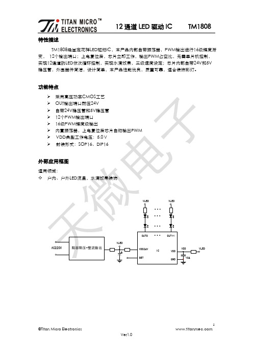
功能特点
采用高压功率CMOS工艺 OUT输出端口耐压24V 自带24V稳压管和5V稳压管 12个PWM输出端口 16级PWM辉度级输出 内置振荡器,上电复位后芯片自动输出PWM VDD典型工作电压:5.0V 封装形式:SOP16、DIP16