synopsys_ic_compiler_介绍、安装、调试和设计流程
Synopsys安装和license制作简易教程

Synopsys 工具安装和 license 制作简易教程Linux virtual machine “Ubuntu_16_04_for_synopsys” Info,Username: jackPassword: login123Memory: 2GBHard disk: 64GBProcessor counts: 1Internet connection mode: NAT安装过程(软件环境:VMware12pro / ubuntu16.04 / 32 位版本;64 位版本运行不成功)事先安装好 VMware12pro 和 ubuntu16.04,之后在 ubuntu 中操作设置 Ubuntu 镜像源如图 1(a)所示,将 ubuntu software->Software & Updates->Download from 设置成中国的网站,设置成功后关闭窗口,不选择更新如图 1(b)所示,在终端中键入命令$ sudo apt-get update 进行更新(a) ubuntu software (b) apt update图 1 ubuntu 镜像源更新安装必要工具键入命令$ sudo apt-get install vim csh dconf-editor libjpeg62-dev设置 Ubuntu 显示中文键入命令$ dconf-editor如图 2 所示,将org->gnome->gedit->preferences->encodings->candidate-encodings 的值设置成['CURRENT', 'ISO-8859-15', 'GB18030', 'UTF-8', 'UTF-16']图 2 dconf-editor键入命令ifconfig,确定网卡名是否为eth0,否则按照下列步骤更改成eth0 键入命令$ su root键入命令# vim /etc/default/grub,在GRUB_CMDLINE_LINUX 中添加net.ifnames=0biosdevname=0,新GRUB_CMDLINE_LINUX 如下GRUB_CMDLINE_LINUX="find_preseed=/preseed.cfg auto noprompt priority=critical locale=en_USnet.ifnames=0 biosdevname=0"键入命令# update-grub键入命令# vim /etc/network/interfaces,添加auto eth0iface eth0 inet dhcp重启系统新建synopsys 工具安装目录,并拷贝安装源tar 压缩包到sources 文件夹下,如图3 所示;同时将installer_v3.2.tar 解压到文件夹installer 中图3 安装目录树以安装Synopsys design compiler, dc 为例,而scl、vcs 和pt 的安装同dc(注:synopsys的其他工具的安装过程都相同)键入命令$ ~/eda/synopsys/installer/setup.sh 开启图形安装界面,如图4(a)所示选择安装源路径为/home/jack/eda/synopsys/sources,如图4(b)所示选择安装syn,即为dc,如图4(c)所示选择安装路径为/home/jack/eda/synopsys/dc,如图4(d)所示其他未说明步骤按默认处理(a) 启动界面(b) 选择安装源路径(c) 选择安装DC (d) 选择安装路径图4 DC 安装过程制作license(注:各种synopsys license 制作包大同小异)键入命令$ ifconfig –a,记录eth0 的MAC 地址在Windows(不一定是本机,也可以是其他电脑)中进行操作,关掉一切杀毒软件运行license 制作包中的LicGen.exe点开Open 按钮,选择synopsys.lpd,如图5(a)所示如图5(b)所示在两处Host ID->Custom 键入eth0 的MAC 地址,点击Generate 生成的内容Save 成synopsys.dat将生成的synopsys.dat 文件保存到Synopsys SSS Feature Keygen 文件夹中打开cmd,进入Synopsys SSS Feature Keygen 目录后运行sssverify.exe synopsys.dat,复制生成的SECRET DATA,如图5(c)和图5(d)打开Synopsys SSS Feature Keygen 文件夹中的KeyGen.exe,如图5(e)所示,键入SECRET DATA 和eth0 的MAC 地址,生成license.dat如图5(f)所示,将license.dat 中的FEATURE SSS 内容粘贴到synopsys.dat 中,如果synopsys.dat 中存在则替换如图5(g)所示,在相应位置修改localhost 和snpslmd path;其中在ubuntu 中键入命令$ hostname 可获取localhost,而snpslmd 后面的链接地址设置成绝对路径~/eda/synopsys/scl/linux/bin/snpslmd(附录A 为synopsys.dat 更改后的部分内容)(a) 选择Synopsys.lpd (b) 生成synopsys.dat(c) 验证synopsys.dat(d) 生成SECRET DATA(e) 生成license.dat(f) license.dat(g) 修改后的synopsys.dat图5 license 制作过程验证license将制作好的license 拷贝到~/eda/synopsys/license 目录下,同时终端进来该目录如图6 所示,键入命令$ ~/eda/synopsys/scl/linux/bin/sssverify synopsys.dat,出现PASSED 表示OK图6 验证license环境变量配置键入命令$ vim ~/.bashrc,添加如图7 所示的环境变量,详见附件B图7 环境变量设置运行每次运行前先键入命令$ lmli2,启动scl,如图8(a)所示键入命令$ dc,启动dc 的图形界面,如图8(b)所示键入命令$ dve,启动vcs 的图形界面,如图8(c)所示键入命令$ pt,启动pt 的图形界面,如图8(d)所示(a) 启动scl(b) dc 的图形界面(c) vcs 的图形界面(d) pt 的图形界面(缺图)图8 运行界面遇到的问题记录1. 如在终端中显示缺什么,就试试安装什么,$ sudo apt-get install *2. lmgrd 找不到$ sudo apt install lsb-core3. grep: /etc/redhat-release: No such file or directory$ sudo > /etc/redhat-release4. /bin/sh: 0: Illegal option –h$ sudo mv /bin/dash /bin/dash~$ sudo ln -s /bin/bash /bin/dash附录ASERVER ubuntu 000c2960189e 27000DAEMON snpslmd /home/jack/eda/synopsys/scl/linux/bin/snpslmdFEATURE SSS snpslmd 1.0 31-dec-2020 uncounted 0EFAB50928B9EDBDB856 \ VENDOR_STRING="69656 d1d88 34cc3 35f9b 39561 08bdd 779a4 23589 \aa9a3 196" HOSTID=000c2960189e ISSUER="Team ZWT 2006" \NOTICE="Licensed to mammoth//ZWT 2006 [PLEASE DO NOT DELETE THIS \ SSS KEY]" SN=RK:1978-0:001224:0 START=1-jan-2006附录B# 添加以下环境变量到~/.bashrc# 适用于32 位,64 位只需将链接中linux 替换成amd64# (以下必选)# synopsysexport SYNOPSYS_HOME=/home/jack/eda/synopsys# licenseexport LM_LICENSE_FILE=$SYNOPSYS_HOME/license/sysnopsys.datexport SNPSLMD_LICENSE_FILE=27000@localhost.localdomain# sclexport SCL_HOME=$SYNOPSYS_HOME/sclexport PATH=$PATH:$SCL_HOME/linux/binalias lmli2="lmgrd -c $LM_LICENSE_FILE -l ~/syn_lic.log"# (以下可选)# vcsexport VCS_HOME=$SYNOPSYS_HOME/vcsexport PATH=$PATH:$VCS_HOME/bin# dcexport DC_HOME=$SYNOPSYS_HOME/dcexport PATH=$PATH:$DC_HOME/binalias dc=design_visionalias dcs=dc_shell# ptexport PT_HOME=$SYNOPSYS_HOME/ptexport PATH=$PATH:$PT_HOME/binalias pt=primetimealias pts=pt_shell# simifexport SIMIF_HOME=$SYNOPSYS_HOME/simif export PATH=$PATH:$SIMIF_HOME/bin# hspiceexport HSPICE_HOME=$SYNOPSYS_HOME/hspice export PATH=$PATH:$HSPICE_HOME/hspice/bin# sxexport SX_HOME=$SYNOPSYS_HOME/sxexport PATH=$PATH:$SX_HOME/binalias sx=sx2007# iccexport ICC_HOME=$SYNOPSYS_HOME/iccexport PATH=$PATH:$ICC_HOME/binalias iccs=icc_shell# herculesexport HERCULES_HOME=$SYNOPSYS_HOME/hercules export PATH=$PATH:$HERCULES_HOME/bin# starrcexport STARRC_HOME=$SYNOPSYS_HOME/starrc export PATH=$PATH:$STARRC_HOME/bin。
Synopsys系列软件安装说明

Synopsys 系列软件破@解及安装配置教程一、生成lic:1、使用Synopsys.src替换EFA LicGen 0.4b\packs目录下的Synopsys.src(此处feature 要全,生成的lic就好用)2、利用LicGen.exe生成synopsys.dat(注意:选custom,并填入hostid)3、在虚拟dos环境下(在windows界面下,使用cmd进入),键入:sssverify synopsys.dat得到SECRET DATA4、在windows界面下,双击KeyGen.exe填入上一步得到的SECRET DATA和第2步使用的hostid。
Generate之后在本目录下会产生一个license.dat文件。
5、将license.dat中的SSS Feature 拷贝到synopsys.dat。
如:FEATURE SSS snpslmd 1.0 31-dec-2020 uncounted AD05306DE9F195C50A3E \VENDOR_STRING="69656 d1d88 34cc3 38a6f 538ce df1f2 30f43 8258f \ecc22 fcf" HOSTID=000ae426dd0d ISSUER="Team ZWT 2006" \NOTICE="Licensed to mammoth//ZWT 2006 [PLEASE DO NOT DELETE THIS \SSS KEY]" SN=RK:1978-0:001224:0 START=1-jan-2006注:若第2步生成的synopsys.dat中有SSS FEATURE,可将其删除。
6、修改synopsys.dat的头两句,如:SERVER <host_name> 000ae426dd0d 27000DAEMON snpslmd /home/eda/linux/bin/snpslmd其中:snpslmd指向SCL的snpslmd。
synopsys iC Compiler II 数据手册说明书
DATASHEETOverview IC Compiler™ II is the industry leading place and route solution that delivers best-in-class quality-of-results (QoR) for next-generation designs across all market verticals and process technologies while enabling unprecedented productivity. IC Compiler II includes innovative for flat and hierarchical design planning, early design exploration, congestion aware placement and optimization, clock tree synthesis, advanced node routing convergence, manufacturing compliance, and signoff closure.IC Compiler II is specifically architected to address aggressive performance, power, area (PPA), and time-to-market pressures of leading-edge designs. Key technologies include a pervasively parallel optimization framework, multi-objective global placement, routing driven placement optimization, full flow Arc based concurrent clock and data optimization, total power optimization, multi-pattern and FinFET aware flow and machine learning (ML) driven optimization for fast and predictive design closure. Advanced Fusion technologies offer signoff IR drop driven optimization, PrimeTime ® delay calculation within IC Compiler II, exhaustive path-based analysis (PBA) and signoff ECO within place and route for unmatched QoR and design convergence. F U S I O N D E S I G N P L A T F O R M PrimeTime, StarRC, PrimePower,IC Validator, RedHawk Analysis Fusion Fusion Compiler IC Compiler II Design Compiler NXT TestMAX F o r m a l i t y ECO Fusion S i g n o f f F u s i o n S i g n o f f F u s i o n Test Fusion Figure 1: IC Compiler II Anchor in Synopsys Design PlatformAccelerating DesignClosure on AdvancedDesignsIC Compiler II Industry Leading Place and Route SystemKey BenefitsProductivity• The highest capacity solution that supports 500M+ instances with a scalable and compact data model• A full suite of design planning features including transparent hierarchical optimization• Out-of-the-box simple reference methodology for easy setup• Multi-threaded and distributed computing for all major flow steps• Golden signoff accuracy with direct access to PrimeTime delay calculationPPA• Unified TNS driven optimization framework• Congestion, timing, and power-driven logic re-synthesis• IEEE 1801 UPF/multi-voltage support• Arc-based concurrent clock and data optimization• Global minima driven total power optimizationAdvanced Nodes• Multi-pattern and FinFET aware design flow• Next generation advanced 2D placement and legalization• Routing layer driven optimization, auto NDR, and via pillar optimization• Machine learning driven congestion prediction and DRC closure• Highest level of foundry support and certification for advanced process nodes• IC Validator in the loop signoff driven DRC validation and fixingAdvanced Fusion Technology• Physically aware logic re-synthesis• IR drop driven optimization during all major flow steps• PrimeTime delay calculation based routing optimization for golden accuracy• Integrated PrimeTime ECO flow during routing optimization for fastest turnaround timeEmpowering Design Across Diversified ApplicationsThe dizzying pace of innovation and highly diversified applications across the design spectrum is forcing a complete rethink of the place and route systems to design and implement differentiated designs in a highly competitive semiconductor market on schedule. Designers on emerging process nodes must meet aggressive PPA and productivity goals. It essentially means efficient and intelligent handling of 100s of millions of place-able instances, multiple levels of hierarchy, 1000s of hard macros, 100s of clocks, wide busses, and 10s of modes and corners power domains and complex design constraints and process technology mandates. Emphasis on Designer ProductivityIC Compiler II is architected from the ground up for speed and scalability. Its hierarchical data model consumes 2-3X less memory than conventional tools, boosting the limits of capacity to 500M placeable instances and beyond. Adaptive abstraction and on-the-fly data management minimize memory requirements and enable fast responsive data manipulation. Near-linear multi-core threading of key infrastructural components and core algorithms such as database access and timing analysis speed up optimization at all phases of design. Patented, lossless compact modeling and independent R and C extraction allow handling more modes and corners (MCMM scenarios) with minimal runtime impact.IC Compiler II has built-in Reference Methodology(RM) that ensures fast flow bring up. This RM Flow is Foundry Process/Design Type specific to ensure a robust starting point and seamless bring up. IC Compiler II has direct access to the Golden PrimeTime delay calculation engine to minimize ECO iterations.IC Compiler II’s new data model enables designers to perform fast exploration and floorplanning with complex layout requirements. IC Compiler II can create bus structures, handle designs with n-levels of physical hierarchy, and support Multiply Instantiated Blocks (MIBs) in addition to global route driven pin assignment/feedthrough flow, timing driven macro placement, MV area design planning.A design data mismatch inferencing engine analyzes the quality of inputs and drives construct creation on the fly, delivering design insights even with “incomplete” data early in the design cycle. Concurrent traversal of logical and physical data models enables hierarchical Data-Flow Analysis (DFA) and fast interactive analysis through multi-level design hierarchies and MIBs. Data flow and feedthrough paths highlighted in Figure 2 allow analysis and manipulation through n-levels of hierarchy to complete early design exploration and prototyping.Figure 2: Fast interactive analysis through multiple-levels of physical hierarchy and MIBPipeline-register-planning shown in Figure 3, provides guidance for optimal placement to meet the stringent timing requirementsof high-performance designs. Interactive route editor integrated which is advanced node aware shown in Figure 4, allows intricate editing and routing functions, including the creation of special signal routes, buses, etc.Figure 3: Pipeline register placement enables superior QoR for designs with complex busesAchieving Best Performance, Power, Area, and TATIC Compiler II features a new optimization framework built on global analytics. This Unified TNS Driven Optimization framework is shared with Design Compiler NXT synthesis to enable physically-aware synthesis, layer assignment, and route-based optimization for improved PPA and TAT. Multi-Corner Multi-Mode (MCMM) and Multi-Voltage (MV) aware, level-based analytical algorithms continuously optimize using parallel heuristic algorithms. Multi-factor costing functions deliver faster results on both broad and targeted design goals. Concurrent PPA driven logic remapping, rewiring, and legalization interleaved with placement minimizes congested logic, resulting in simple localized logic cones that maximize routability and QoR.IC Compiler II minimizes leakage with fast and efficient cell-by-cell power selection across HVT, SVT and LVT cells and varying channel lengths. Activity-driven power optimization uses VCD/ SAIF, net toggle rates, or probability functions to drive placement decisions and minimize pin capacitances. Multi-bit register banking optimizes clock tree structures, reduces area, and net length, while automatically managing clock, data, and scan chain connections.Advanced modeling of congestion across all layers highlighted in Figure 4 provides accurate feedback throughput the flow from design planning to post- route optimization.Figure 4: Intelligent and accurate analysis for congestion and powerIC Compiler II introduces a new Concurrent Clock and Data (CCD) analysis and optimization engine that is built-in to every flow step resulting in meeting both aggressive performance and minimizing total power footprint. ARC-based CCD optimization performs clock tree traversal across all modes/corners in path-based fashion to ensure optimal delay budgeting.Robust support for clock distribution enables virtually any clock style, including mesh, multi-source, or H-tree topologies. Advanced analysis and debugging features perform accurate clock QoR analysis and debugging as highlighted in Figure 5.Figure 5: Accurate clock QoR analysis and debugging (a & b) Abstracted clock graph and schematic.(c) Latency clock graph. (d) Colored clock tree in layout.IC Compiler II features many innovative technologies that make it the ideal choice for high-performance, energy-efficient Arm®processor core implementation, resulting in industry-best milliwatts/megahertz (mW/MHz) for mobile and other applications across the board. Synopsys and Arm work closely together to offer optimized implementation of popular Arm cores for IC Compiler II,with reference flows available for Arm Cortex®-A high-performance processors and Mali GPUs. In addition, Arm offers off-the-shelf Artisan® standard cell and memory models that have been optimally tuned and tested for fast deployment in an IC Compiler II environment. Continuous technology innovation and close collaboration makes IC Compiler II the leading choice for Arm-based high- performance design.Highest Level of Advanced Node Certification and SupportIC Compiler II provides advanced node design enablement across major foundries and technology nodes—including 16/14nm,12/10nm, 7/5nm, and sub-5nm geometries. Zroute digital router technology ensures early and full compliance with the latest design rules required for these advanced node technologies. Synopsys collaborates closely with all the leading foundries to ensure that IC Compiler II is the first to deliver support for early prototype design rules and support for the final production design rules. IC Compiler II design technologies maximize the benefits of new process technologies and offer optimal return on investment for cutting-edge silicon applications.IC Compiler II advanced node design support includes multi-pattern/FinFET aware placement and routing, Next-generation advanced 2D placement and legalization, routing layer driven optimization, auto NDR, and via pillar optimization. IC Validator in the loop provides signoff DRC feedback during Implementation.Foundry fill Track based fillFigure 6: IC Validator In-Design metal fill color aware metal fill, optimized for density and foundry requirementsMachine learning driven congestion prediction and DRC closure allow for fastest routing convergence with best PPA. Multiple sets of training data are used to extract key predictive elements that guide the pre-route flow.Advanced Fusion TechnologyThe Fusion Design Platform™ delivers unprecedented full-flow QoR and time-to-results (TTR) to accelerate the next wave of semiconductor industry innovation. The industry’s first AI-enhanced, cloud-ready Design Platform with Fusion Technology™ isbuilt from Synopsys’ market-leading, massively-parallel digital design tools, and augmented with innovative capabilities to tacklethe escalating challenges in cloud computing, automotive, mobile, and IoT market segments and accelerate the next wave of industry innovation.Fusion Technology redefines conventional EDA tool boundaries across synthesis, place-and-route, and signoff, sharing integrated engines across the industry’s premier digital design products. It enables designers to accelerate the delivery of their next-generation designs with the industry-best QoR and the TTR.©2019 Synopsys, Inc. All rights reserved. Synopsys is a trademark of Synopsys, Inc. in the United States and other countries. A list of Synopsys trademarks isavailable at /copyright.html . All other names mentioned herein are trademarks or registered trademarks of their respective owners.。
Synopsys系列工具简介
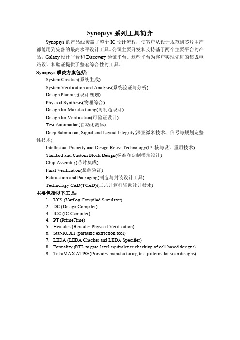
Synopsys系列工具简介Synopsys的产品线覆盖了整个IC设计流程,使客户从设计规范到芯片生产都能用到完备的最高水平设计工具。
公司主要开发和支持基于两个主要平台的产品,Galaxy设计平台和Discovery验证平台。
这些平台为客户实现先进的集成电路设计和验证提供了整套综合性的工具。
Synopsys解决方案包括:System Creation(系统生成)System Verification and Analysis(系统验证与分析)Design Planning(设计规划)Physical Synthesis(物理综合)Design for Manufacturing(可制造设计)Design for Verification(可验证设计)Test Automation(自动化测试)Deep Submicron, Signal and Layout Integrity(深亚微米技术、信号与规划完整性技术)Intellectual Property and Design Reuse Technology(IP 核与设计重用技术)Standard and Custom Block Design(标准和定制模块设计)Chip Assembly(芯片集成)Final Verification(最终验证)Fabrication and Packaging(制造与封装设计工具)Technology CAD(TCAD)(工艺计算机辅助设计技术)主要包括以下工具:1.VCS (Verilog Compiled Simulator)2.DC (Design Compiler)3.ICC (IC Compiler)4.PT (PrimeTime)5.Hercules (Hercules Physical Verification)6.Star-RCXT (parasitic extraction tool)7.LEDA (LEDA Checker and LEDA Specifier)8.Formality (RTL to gate-level equivalence checking of cell-based designs)9.TetraMAX ATPG (Provides manufacturing test patterns for scan designs)1.VCS (Verilog Compiled Simulator)VCS是编译型Verilog模拟器,它完全支持OVI标准的Verilog HDL语言、PLI和SDF。
IC设计流程-synopsys

D Z KIC设计流程--基于synopsys EDA tools一、数字IC的设计流程:图一数字IC设计流程1、立项,市场调研基本是由市场和你的老板负责制定。
2、一旦立项后下面该做的是制定spec也就是各项参数和性能,以及划分模块,验证以及协调。
3、下面就开始轮到前端的人员来干活了。
(1)首先前端人员吃时候要开始撰写你的code也就是要开始写你的RTL代码(指的是你要用来生成电路的代码),和测试代码(也就是testbench)。
业界基本是在linux下的vim中编写好各个模块的verilog文档(当然大的模块尽可能划分成许多小的模块)。
当然测试向量的编写可以通过designer的手工编写(一般采用),也可以辅助用TetraMAX 生成。
(2)接下来是验证你的代码是否语法、功能等正确此事后D Z KVCS便是用来simulation你的代码的。
如果不正确再回到vim中修改,直到RTL代码满足要求(神仙才有可能第一版就能合格的)。
(3)下面就要开始将你的RTL代码转换成门级电路的时刻了,一般业界用的design compiler (DC),但是对你的设计有什么约束就要根据各自的设计思路和经验去下constrain(一些可以通过手写编辑文档,一部分可以通过DC中的gui界面去点击,当然最终全面的文档可以通过DC吐出来)。
此时也是需要你插入scan chain的时候。
最后在工具综合满足你的面积和时序要求下可以吐出门级的verilog网表。
『此地需要fab提供standcell或者IP核的lib和db以及sdb(也可用dc中默认的,不过不推荐)等文件』(4)拿到门级的verilog网表并不代表你就直接可以用它去参与bkend工作了,现在的soc一般需要做大量的验证工作,首先是形式验证,检验你综合的门级网表是否偏离了你的设计意图。
此时用的工具是Formality;其次是静态时序分析,验证你的门级网表是否在时序上满足设计要求,此时用到的工具是PrimeTime(PT)。
Synopsys OptoDesigner 2020.09安装指南说明书
3. Troubleshooting scanning issues........................................................25
Accidental full scan proliferation by folder paths which include build or commit ID............................ 25 Solution......................................................................................................................................25
Contents
Contents
Preface....................................................................................................5
1. Scanning best practices......................................................................... 8
集成电路设计流程中的EDA工具使用教程
集成电路设计流程中的EDA工具使用教程综合电路设计是电子工程师在集成电路设计中经常进行的一项重要任务。
通过使用EDA(电子设计自动化)工具,设计师能够更高效地完成设计流程。
本文将介绍集成电路设计流程中常用的EDA工具及其使用方法。
一、设计综合工具设计综合是集成电路设计流程中的第一步,它将高级硬件描述语言(如VHDL或Verilog)转换为逻辑网表。
常用的设计综合工具包括Synopsys Design Compiler、Cadence Genus等。
设计综合工具能够根据设计规范和约束,实现功能实现和性能优化。
在使用设计综合工具时,首先需要准备好设计规范和约束文件,以确保综合结果能够满足设计要求。
然后,通过命令行或图形界面界面加载设计文件,设置综合选项并运行综合流程。
二、逻辑综合工具逻辑综合是将逻辑网表转换为标准单元库的过程,并执行功耗优化和时序约束等操作。
常用的逻辑综合工具包括Synopsys Design Compiler、Cadence Genus等。
在使用逻辑综合工具时,首先需要准备好逻辑网表文件和约束文件。
然后,通过命令行或图形界面界面加载设计和约束文件,设置综合选项,并运行逻辑综合流程。
逻辑综合工具还可以生成时序分析所需的约束文件,并进行时序分析。
三、布局布线工具布局布线是在物理空间中放置和布线所有电路元件的过程,以满足电路设计的约束条件。
布局布线工具能够根据设计规范和约束,生成良好的物理布局和可靠的布线。
常用的布局布线工具包括Cadence Innovus、SynopsysIC Compiler等。
在使用布局布线工具时,首先需要准备好物理约束文件和逻辑网表。
然后,通过命令行或图形界面界面加载设计和约束文件,设置布局布线选项,并运行布局布线流程。
布局布线工具还可以执行时序优化操作,以满足时序约束。
四、仿真工具仿真是验证电路设计功能和性能的关键步骤。
通过使用仿真工具,设计师可以在真实环境中模拟电路行为,并对其进行调试和优化。
synopsys EDA工具安装和调试
摘要:本文以美国 Synopsys SOC 一体化设计软件的应用环境为实例,基于当前通用的 Solaris-UNIX 局域网环境,系统地阐述 IC 设计工程软件在网络环境中的典型系统配置、安全保障及系统维护技术。
文章给出了超大规模集成电路自动化设计工程软件的常规配置方案,对从事 IC 自动化设计网络环境管理的技术工作者具有较强的可操作性和可借鉴作用。
关键词:超大规模集成电路;片上系统;超深亚微米;电子设计自动化;计算机辅助设计中图分类号:TN43 文献标识码: B 文章编号:1003-0107(2004) 08引言实施超大规模集成电路(ULSI)及片上系统(SOC)一体化设计工程,基于三点:先进的 IC 设计工程软件;高配置的操作系统及网络设备;最佳的、高安全性的软件运行环境。
先进的 IC 设计工程软件以美国 Synopsys SOC 一体化设计软件为技术支持。
高配置的计算机网络设备全面满足软件的运行要求。
当前,最为薄弱的是软件运行环境技术性维护和软件运行的安全性保障问题。
这一点,也是诸多集成电路设计公司最为重视的。
美国 Synopsys SOC 一体化设计软件在中国的用户增长极快。
基于此,以当前通用的 Sol aris-UNIX 局域网环境为基本网络配置,研讨并提出合理的 IC 设计工程软件系统配置、安全保障及系统维护的技术方案,是本文的主要议题。
以下的讨论将给出典型的 IC 自动化设计工程软件的常规配置方案及通用的网络环境管理技术,期望着能给 IC 设计工程网络环境的技术维护工作者以较强的借鉴作用。
一 IC 设计工程软件的常规网络环境配置超大规模集成电路( ULSI )设计对设计软件的运行环境要求极高,突出表现在仿真工程的庞大计算量及操作系统的高安全性。
基于此,该系列软体更多地采用 Unix操作系统。
通常,大多采用SUN-Server -Workstation系统。
SUN-Unix的当前版本是Solaris-9.0,Solaris-9.0为64位操作系统。
synopsys ic compiler 介绍、安装、调试和设计流程
synopsys ic compiler 介绍、安装、调试和设计流程加入该小组相关分类:petery (组长) 2007/9/23 顶楼举报一、介绍synopsys ic compiler (v2005.linux)是基于Galaxy设计平台开发的产品。
主要的工具有:LEDALEDA是可编程的语法和设计规范检查工具,它能够对全芯片的VHDL和Verilog描述、或者两者混合描述进行检查,加速SoC的设计流程。
LEDA预先将IEEE可综合规范、可仿真规范、可测性规范和设计服用规范集成,提高设计者分析代码的能力VCSVCS是编译型Verilog模拟器,它完全支持OVI标准的Verilog HDL语言、PLI和SDF。
VCS具有目前行业中最高的模拟性能,其出色的内存管理能力足以支持千万门级的ASIC设计,而其模拟精度也完全满足深亚微米ASIC Sign-Off 的要求。
VCS结合了节拍式算法和事件驱动算法,具有高性能、大规模和高精度的特点,适用于从行为级、RTL到Sign-Off等各个阶段。
VCS已经将CoverMeter 中所有的覆盖率测试功能集成,并提供VeraLite、CycleC等智能验证方法。
VCS 和Scirocco也支持混合语言仿真。
VCS和Scirocco都集成了Virsim图形用户界面,它提供了对模拟结果的交互和后处理分析。
SciroccoScirocco是迄今为止性能最好的VHDL模拟器,并且是市场上唯一为SoC验证度身定制的模拟工具。
它与VCS一样采用了革命性的模拟技术,即在同一个模拟器中把节拍式模拟技术与事件驱动的模拟技术结合起来。
Scirocco的高度优化的VHDL编译器能产生有效减少所需内存,大大加快了验证的速度,并能够在一台工作站上模拟千万门级电路。
这一性能对要进行整个系统验证的设计者来说非常重要。
VeraVera验证系统满足了验证的需要,允许高效、智能、高层次的功能验证。
synopsys工具安装教程
synopsys⼯具安装教程前⾔:这是本⼈经过两个星期的奋⽃,从对linux命令的⽣涩到熟练,对后端⼯具的陌⽣到熟悉的⼀段战⽃史下⾯我把我的操作过程详细写下,供⼤家学习参考!!⼀:准备⼯作所需平台1、vmware92、RHEL(红帽企业版)6.3Synopsys ⼯具1、installer_v3.0(安装synopsys EDA tools 的图形界⾯的安装⼯具)2、scl_10.9.3(synopsys license 管理⼯具,⽤于启动tools 的features)3、dc_2009.06(逻辑综合⼯具)4、icc_2009.06(布局布线⼯具)5、pt_2012.12(时序分析⼯具)License⽣成⼯具1、EFA LicGen 0.4b2、Synopsys SSS Feature Keygen3、Synposys.src(最新的据我所知是40kb⼤⼩,有⽐较全的features)⼆:搭建RHEL1、安装vmware:本章节详见另⼀个⽂档。
⽂档名为“vmware安装⼿册”。
还有⼀份汉化包,需要可⾃⾏下载。
2、安装RHEL:本章详见另⼀个⽂档。
⽂档名为“RHEL6.3安装⼿册”。
Ps:有⼀个页⾯会让你选择安装的软件包,这个时候⼈⼯勾上所有的软件包,不然启eda ⼯具的时候会发现很多系统库找不到。
三:vmware tools安装1、以root⽤户进⼊linux,找到左上⾓的VM选项,下拉之后选择安装wmwaretools。
过⼀会⼉会弹出来⼀个框框,显⽰vmwaretools-9.2.2-893683.tar.gz然后新开⼀个终端,输⼊cd /media 你会看到vmwaretools-9.2.2-893683.tar.gz就在那⾥。
然后把他拷贝出来,后解压安装。
具体命令可以⽹上搜索。
四:license制作License制作要⽤到上述的材料,具体详见另⼀个⽂档。
⽂档名为“license制作”。
- 1、下载文档前请自行甄别文档内容的完整性,平台不提供额外的编辑、内容补充、找答案等附加服务。
- 2、"仅部分预览"的文档,不可在线预览部分如存在完整性等问题,可反馈申请退款(可完整预览的文档不适用该条件!)。
- 3、如文档侵犯您的权益,请联系客服反馈,我们会尽快为您处理(人工客服工作时间:9:00-18:30)。
synopsys ic compiler 介绍、安装、调试和设计流程加入该小组相关分类:petery (组长) 2007/9/23 顶楼举报一、介绍synopsys ic compiler (v2005.linux)是基于Galaxy设计平台开发的产品。
主要的工具有:LEDALEDA是可编程的语法和设计规范检查工具,它能够对全芯片的VHDL和Verilog描述、或者两者混合描述进行检查,加速SoC的设计流程。
LEDA预先将IEEE可综合规范、可仿真规范、可测性规范和设计服用规范集成,提高设计者分析代码的能力VCSVCS是编译型Verilog模拟器,它完全支持OVI标准的Verilog HDL语言、PLI和SDF。
VCS具有目前行业中最高的模拟性能,其出色的内存管理能力足以支持千万门级的ASIC设计,而其模拟精度也完全满足深亚微米ASIC Sign-Off的要求。
VCS结合了节拍式算法和事件驱动算法,具有高性能、大规模和高精度的特点,适用于从行为级、RTL到Sign-Off等各个阶段。
VCS已经将CoverMeter中所有的覆盖率测试功能集成,并提供VeraLite、CycleC等智能验证方法。
VCS和Scirocco也支持混合语言仿真。
VCS和Scirocco都集成了Virsim图形用户界面,它提供了对模拟结果的交互和后处理分析。
SciroccoScirocco是迄今为止性能最好的VHDL模拟器,并且是市场上唯一为SoC验证度身定制的模拟工具。
它与VCS 一样采用了革命性的模拟技术,即在同一个模拟器中把节拍式模拟技术与事件驱动的模拟技术结合起来。
Scirocco的高度优化的VHDL编译器能产生有效减少所需内存,大大加快了验证的速度,并能够在一台工作站上模拟千万门级电路。
这一性能对要进行整个系统验证的设计者来说非常重要。
VeraVera验证系统满足了验证的需要,允许高效、智能、高层次的功能验证。
Vera验证系统已被Sun、NEC、Cisco等公司广泛使用以验证其实际的产品,从单片ASIC到多片ASIC组成的计算机和网络系统,从定制、半定制电路到高复杂度的微处理器。
Vera验证系统的基本思想是产生灵活的并能自我检查的测试向量,然后将其结合到test-bench中以尽可能充分测试所设计的电路。
Vera验证系统适用于功能验证的各个层次,它具有以下特点:与设计环境的紧密集成、启发式及全随机测试、数据及协议建模、功能代码覆盖率分析。
Physical CompilerPhysical Compiler解决0.18微米以下工艺技术的IC设计环境,是Synopsys物理综合流程的最基本的模块,它将综合、布局、布线集成于一体,让RTL设计者可以在最短的时间内得到性能最高的电路。
通过集成综合算法、布局算法和布线算法。
在RTL到GDS II的设计流程中,Physical Compiler向设计者提供了可以确保即使是最复杂的IC设计的性能预估性和时序收敛性。
Clocktree CompilerClockTree Compiler是嵌入于Physical Compiler的工具,它帮助设计者解决深亚微米IC设计中时钟树的时序问题。
它不仅能够简化设计流程,而且可以极大的提高时钟树的质量:对于插入延时有5%-20%的改进,对时钟偏移有5%-10%的改进。
DC-ExpertDC得到全球60多个半导体厂商、380多个工艺库的支持。
据最新Dataquest的统计,Synopsys的逻辑综合工具占据91%的市场份额。
DC是十二年来工业界标准的逻辑综合工具,也是Synopsys最核心的产品。
它使IC设计者在最短的时间内最佳的利用硅片完成设计。
它根据设计描述和约束条件并针对特定的工艺库自动综合出一个优化的门级电路。
它可以接受多种输入格式,如硬件描述语言、原理图和网表等,并产生多种性能报告,在缩短设计时间的同时提高设计性能。
DC Ultra对于当今所有的IC设计,DC Ultra 是可以利用的最好的综合平台。
它扩展了DC Expert的功能,包括许多高级的综合优化算法,让关键路径的分析和优化在最短的时间内完成。
在其中集成的Module Compiler数据通路综合技术, DC Ultra利用同样的VHDL/Verilog流程,能够创造处又快又小的电路。
DFT CompilerDFT Compiler提供独创的“一遍测试综合”技术和方案。
它和Design Compiler 、Physical Compiler系列产品集成在一起的,包含功能强大的扫描式可测性设计分析、综合和验证技术。
DFT Compiler可以使设计者在设计流程的前期,很快而且方便的实现高质量的测试分析,确保时序要求和测试覆盖率要求同时得到满足。
DFT Compiler同时支持RTL级、门级的扫描测试设计规则的检查,以及给予约束的扫描链插入和优化,同时进行失效覆盖的分析。
Power CompilerPower Compiler?提供简便的功耗优化能力,能够自动将设计的功耗最小化,提供综合前的功耗预估能力,让设计者可以更好的规划功耗分布,在短时间内完成低功耗设计。
Power Compiler嵌入DesignCompiler/Physical Compiler之上,是业界唯一的可以同时优化时序、功耗和面积的综合工具。
FPGA Compiler IIFPGA Compiler II是一个专用于快速开发高品质FPGA产品的逻辑综合工具,可以根据设计者的约束条件,针对特定的FPGA结构(物理结构)在性能与面积方面对设计进行优化,自动地完成电路的逻辑实现过程,从而大大降低了FPGA设计的复杂度。
FPGA Compiler II利用了特殊的结构化算法,结合高层次电路综合方法,充分利用复杂的FPGA结构将设计输入综合成为满足设计约束条件,以宏单元或LUT为基本模块的电路,可以多种格式输出到用户的编程系统中。
FPGA Compiler II为FPGA设计者提供高层次设计方法,并为IC设计者用FPGA 做样片而最后转换到ASIC提供了有效的实现途径。
Prime Power动态功耗的门级仿真和分析的工具,可精确分析基于门级的设计的功耗问题,逐渐成为ASIC和对功耗要求较高的结构定制产品(袖珍计算机和通讯设备)设计者的高级解决方案。
PrimeTimePrimeTime® 是针对复杂、百万门芯片进行全芯片、门级静态时序分析的工具。
PrimeTime可以集成于逻辑综合和物理综合的流程,让设计者分析并解决复杂的时序问题,并提高时序收敛的速度。
PrimeTime是众多半导体厂商认可的、业界标准的静态时序分析工具。
FormalityFormality是高性能、高速度的全芯片的形式验证:等效性检查工具。
它比较设计寄存器传输级对门级或门级对门级来保证它没有偏离原始的设计意图。
在一个典型的流程中,用户使用形式验证比较寄存器传输级源码与综合后门级网表的功能等效性。
这个验证用于整个设计周期,在扫描链插入、时钟树综合、优化、人工网表编辑等等之后,以便在流程的每一阶段都能在门级维持完整的功能等效。
这样在整个设计周期中就不再需要耗时的门级仿真。
将Formality和PrimeTime这两种静态验证方法结合起来,一个工程师可以在一天内运行多次验证,而不是一天或一周只完成一次动态仿真验证。
SaberSaber是Synopsys公司开发并于1987年推出的模拟及混合信号仿真软件,被誉为全球最先进的系统仿真软件,也是唯一的多技术、多领域的系统仿真产品。
与传统仿真软件不同,Saber在结构上采用硬件描述语言(MAST)和单内核混合仿真方案,并对仿真算法进行了改进,使Saber仿真速度更快、更加有效、应用也越来越广泛。
应用工程师在进行系统设计时,建立最精确、最完善的系统仿真模型是至关重要的。
Saber可同时对模拟信号、事件驱动模拟信号、数字信号以及模数混合信号设备进行仿真。
利用Synopsys 公司开发的Calaversas算法,Saber可以确保同时进行的两个仿真进程都能获得最大效率,而且可以实现两个进程之间的信息交换,并在模拟和数字仿真分析之间实现了无缝联接。
Saber适用领域广泛,包括电子学、电力电子学、电机工程、机械工程、电光学、光学、水利、控制系统以及数据采样系统等等。
只要仿真对象能够用数学表达式进行描述,Saber就能对其进行系统级仿真。
在Saber中,仿真模型可以直接用数学公式和控制关系表达式来描述,而无需采用电子宏模型表达式。
因此,Saber可以对复杂的混合系统进行精确的仿真,仿真对象不同系统的仿真结果可以同时获得。
为了解决仿真过程中的收敛问题,Saber内部采用5种不同的算法依次对系统进行仿真,一旦其中某一种算法失败,Saber将自动采用下一种算法。
通常,仿真精度越高,仿真过程使用的时间也越长。
普通的仿真软件都不得不在仿真精度和仿真时间上进行平衡。
Saber采用其独特的设计,能够保证在最少的时间内获得最高的仿真精度。
Saber工作在SaberDesigner图形界面环境下,能够方便的实现与Cadence Design System和Mentor Graphics的集成。
通过上述软件也可以直接调用Saber进行仿真。
JupiterXT芯片设计者在层次化物理设计环境中完成从门级网表到布局布线收敛的重要工具,可以帮助您将Timing、Area 和Power与您的设计进行匹配,JupiterXT通过下面的方法来管理和优化您的设计:1、物理版图的层次化管理2、精确的面积、寄生参数和时序估计3、层次化布局布线流程中,精确的子模块时序加载AstroAstro是Synopsys为超深亚微米IC设计进行设计优化、布局、布线的设计环境。
Astro可以满足5千万门、时钟频率GHz、在0.10及以下工艺线生产的SoC设计的工程和技术需求。
Astro高性能的优化和布局布线能力主要归功于Synopsys在其中集成的两项最新技术:PhySiSys和Milkyway DUO结构。
Design VisionSynopsys综合环境的图形界面,在通用技术层和门级进行设计浏览和分析的分析工具。
Mars-railMars-Rail用于功耗和电漂移的分析和优化,以完成低功耗高可靠性的设计。
它将自动在Apollo-II的布局布线中起作用。
Mars-xtalkMars-Xtalk可以进行充分的串扰分析,并能够进行防止串扰发生的布局和布线,解决超深亚微米芯片设计中的信号完整性问题。
CosmosLE/SESynopsys的Cosmos解决方案可以进行自前向后的混合信号、全定制IC设计。
它可以很好的处理自动化的设计流程和设计的灵便性,使得设计周期可以缩短数周甚至几个月。