113R,AL,113R,BK,113R,GY, 规格书,Datasheet 资料
SLM-140;SLM-150;SLM-160;SLM-170;SLM-180;中文规格书,Datasheet资料

H .815 (20.7mm) .835 (21.2mm) .855 (21.7mm) .875 (22.2mm) .895 (22.7mm) .915 (23.2mm) .935 (23.7mm) .955 (24.3mm) .975 (24.8mm) .995 (25.3mm) 1.015 (25.8mm) 1.035 (26.3mm)
CHECKED:
04/23/03
DATE:
SLM-XXX
D
CAGE CODE : 32559
SHEET # 1 OF 1
D. Green
04/23/03
CAD GENERATED DOCUMENT, DO NOT MEASURE DRAWING., CA. 92618
M. C. M. C. M. C.
0.100 [2.5mm] Ø.250 [Ø6.4mm] Ø.290 [Ø7.4mm]
H 0.15 [3.8mm] SH REF. Ø.230 [Ø5.8mm] Ø.045 [Ø1.1mm] TYP. CATHODE I.D. MARKING 0.025 [0.6mm]
H .425 (10.8mm) .435 (11.0mm) .445 (11.3mm) .455 (11.6mm) .465 (11.8mm) .475 (12.1mm) .485 (12.3mm) .495 (12.6mm) .505 (12.8mm) .515 (13.1mm) .525 (13.3mm) .535 (13.6mm) .545 (13.8mm) .555 (14.1mm)
PART NO. SLM-420 SLM-430 SLM-440 SLM-450 SLM-470 SLM-490 SLM-510 SLM-530 SLM-550 SLM-570 SLM-590 SLM-610 SLM-630 SLM-650
MDL-ACIM;中文规格书,Datasheet资料
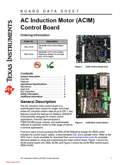
AC Induction Motor (ACIM) Control BoardOrdering InformationContentsGeneral Description. . . . . . . . . . . . . . . . . . . . 1Overview . . . . . . . . . . . . . . . . . . . . . . . . . . . . . 2Features. . . . . . . . . . . . . . . . . . . . . . . . . . . . . . 2Operational Specifications . . . . . . . . . . . . . . 2Mechanical. . . . . . . . . . . . . . . . . . . . . . . . . . . . 3Heat Sink. . . . . . . . . . . . . . . . . . . . . . . . . . . . . 4Bus Capacitors . . . . . . . . . . . . . . . . . . . . . . . . 4Safety Information. . . . . . . . . . . . . . . . . . . . . 4Additional Information . . . . . . . . . . . . . . . . . 4General DescriptionThe AC induction motor control board is asophisticated motor control for single- and three-phase AC induction motors rated at up to 230V. Key features include the feature-rich Stellaris LM3S818 microcontroller designed for motion control applications, Fairchild Semiconductor'sFSBS10CH60 power module, and sophisticated software to optimally control a wide range of motors in diverse applications.First-time users should purchase the RDK-ACIM Reference Design Kit (RDK) whichincludes the control board, cables, a documentation CD, and a sample motor. Refer to the RDK User's Guide (available for download from ) for complete technical details on using and customizing the motor control board. Figure 1 shows the ACIM control board only (MDL-ACIM) and Figure 2 shows the ACIM RDK control board (RDK-ACIM).Order No.DescriptionMDL-ACIMStellaris® ACIM Control Board OnlyRDK-ACIMStellaris® ACIM Control Board Reference Design Kit (includesMDL-ACIM board)Figure 1.ACIM Control Board OnlyFigure 2.ACIM RDK Control BoardOverviewThe MDL-ACIM motor control board controls three-phase and single-phase AC induction motors. The board has an integrated USB port (Virtual COM port) and logic-level serial port connections along with a quadrature encoder/tachometer input for speed and position monitoring. Extensive configuration options using Windows Graphical User Interface (GUI) are available and the board is easy to customize—full source code and design files are available.FeaturesThe MDL-ACIM motor control board provides the following features:End-user customizable line filter, bus capacitors, and JTAG interfaceSplit low-side current sensing for accurate current sensingDynamic braking circuitActive in-rush control circuitElectrically isolated JTAG port for software debugging or production programming (RDK only)Integrated AC line filter (RDK only)USB/Serial UART–FTDI FT232R USB to serial UART–Virtual COM port, 115.2k,8,n,1 operation–Stellaris MCC protocolOperational SpecificationsTable 1 shows the operating parameters for the MDL-ACIM motor control board.Table 1.MDL-ACIM Operating SpecificationsParameter Name Min Nom Max UnitAC Input Voltage (50/60Hz)230V operation195230265V AC 115V w/ voltage doubler95115135V ACDC Bus Voltage270320370V DC Frequency Range0400Hz Continuous Output Current 3.2A RMS Electrical Isolation2500V RMS Supply Current10A RMS Operating Temperature Range0–70°C Storage Temperature Range-25–85°C Digital Input Low Level Input Voltage-0.3 1.3V DCTable 1.MDL-ACIM Operating Specifications (Continued)Parameter Name Min Nom Max Unit Digital Input High Level Input Voltage 2.0 5.0V DC MechanicalFigure 3 shows the mechanical drawing for the MDL-ACIM.PCB size: 3.65" x 4.55" (93mm x115mm)Heatsink is required (MDL-ACIM only)Bus capacitors are required (MDL-ACIM only)Motor connector on PCB–RIA Connect part #31262104Power connector on PCB–RIA Connect part #31262102Figure 3.MDL-ACIM Mechanical DiagramHeat SinkThe ACIM motor module does not come with a heatsink like the RDK-ACIM, but does require a heatsink for operation. Underwriters Laboratories (UL) standards generally require that surfaces that could be touched by a user or service person must not exceed 70°C, so this must be considered when choosing the size material of the heatsink.Bus CapacitorsThe ACIM motor module requires that the customer supply bus capacitors for the board. The recommended capacitors to use are 1500uF, 200V electrolytic capacitors. Safety InformationWARNING – Risk of Electric ShockThe microcontroller in the RDK is not referenced to ground; it is at AC line potential. Do not make direct connection to the JTAG header or any other microcontroller-related circuit. Read the Quickstart Guide first for additional warnings.This RDK operates from AC line voltage. Improper use or application carries electric shock, fire, and other risks that may result in serious injury or death. Please read and follow these safety notices:This documentation and kit must only be used by people with training and experience in working with voltage potentials up to 230 V.The control board has both high-voltage potential and safety low-voltage sections.Do not connect high-voltage potential circuits to safety low-voltage circuits or to ground-referenced equipment such as computers or test equipment.After power is removed, high voltages remain until the bus capacitors discharge. Wait at least one minute after removing power before working with high-voltage circuitry.Use caution when using the on-board controls to adjust motor speed etc. High-voltage circuits are in close proximity.Never perform work on the control board, motor or, wiring while power is applied. Always wear eye protection and use care when operating the motor.In addition to safety risks, other factors that may damage the control hardware, the motor, and its load include improper configuration, wiring, or software. Minimize the risk of damage by following these guidelines.Additional InformationThe following documents are available for download at :RDK-ACIM User’s Manual, Publication Number RDK-ACIM-UMRDK-ACIM QuickstartCopyright © 2008–2009 Texas Instruments, Inc. All rights reserved. Stellaris and StellarisWare are registered trademarks of TexasInstruments. ARM and Thumb are registered trademarks, and Cortex is a trademark of ARM Limited. Other names and brands may be claimed as the property of others.RDK-ACIM-DS-01August 10, 2009Important NoticeTexas Instruments Incorporated and its subsidiaries (TI) reserve the right to make corrections, modifications, enhancements,improvements, and other changes to its products and services at any time and to discontinue any product or service without notice. Customers should obtain the latest relevant information before placing orders and should verify that such information is current and complete. All products are sold subject to TI’s terms and conditions of sale supplied at the time of order acknowledgment.TI warrants performance of its hardware products to the specifications applicable at the time of sale in accordance with TI’s standard warranty. Testing and other quality control techniques are used to the extent TI deems necessary to support this warranty. Except where mandated by government requirements, testing of all parameters of each product is not necessarily performed.TI assumes no liability for applications assistance or customer product design. Customers are responsible for their products and applications using TI components. To minimize the risks associated with customer products and applications, customers should provide adequate design and operating safeguards.TI does not warrant or represent that any license, either express or implied, is granted under any TI patent right, copyright, mask work right, or other TI intellectual property right relating to any combination, machine, or process in which TI products or services are used. Information published by TI regarding third-party products or services does not constitute a license from TI to use such products or services or a warranty or endorsement thereof. Use of such information may require a license from a third party under the patents or other intellectual property of the third party, or a license from TI under the patents or other intellectual property of TI.Reproduction of TI information in TI data books or data sheets is permissible only if reproduction is without alteration and isaccompanied by all associated warranties, conditions, limitations, and notices. Reproduction of this information with alteration is an unfair and deceptive business practice. TI is not responsible or liable for such altered documentation. Information of third parties may be subject to additional restrictions.Resale of TI products or services with statements different from or beyond the parameters stated by TI for that product or service voids all express and any implied warranties for the associated TI product or service and is an unfair and deceptive business practice. TI is not responsible or liable for any such statements.TI products are not authorized for use in safety-critical applications (such as life support) where a failure of the TI product would reasonably be expected to cause severe personal injury or death, unless officers of the parties have executed an agreementspecifically governing such use. Buyers represent that they have all necessary expertise in the safety and regulatory ramifications of their applications, and acknowledge and agree that they are solely responsible for all legal, regulatory and safety-related requirements concerning their products and any use of TI products in such safety-critical applications, notwithstanding anyapplications-related information or support that may be provided by TI. Further, Buyers must fully indemnify TI and its representatives against any damages arising out of the use of TI products in such safety-critical applications.TI products are neither designed nor intended for use in military/aerospace applications or environments unless the TI products are specifically designated by TI as military-grade or "enhanced plastic." Only products designated by TI as military-grade meet military specifications. Buyers acknowledge and agree that any such use of TI products which TI has not designated as military-grade is solely at the Buyer's risk, and that they are solely responsible for compliance with all legal and regulatory requirements in connection with such use.TI products are neither designed nor intended for use in automotive applications or environments unless the specific TI products are designated by TI as compliant with ISO/TS 16949 requirements. Buyers acknowledge and agree that, if they use any non-designated products in automotive applications, TI will not be responsible for any failure to meet such requirements.Following are URLs where you can obtain information on other Texas Instruments products and application solutions:Mailing Address: Texas Instruments, Post Office Box 655303, Dallas, Texas 75265Copyright © 2009, Texas Instruments IncorporatedProducts Applications AmplifiersAudio/audioData Converters Automotive /automotive DLP® Products Broadband /broadband DSPDigital Control /digitalcontrol Clocks and Timers /clocks Medical /medical Interface Military/militaryLogic Optical Networking /opticalnetwork Power Mgmt Security /security Microcontrollers Telephony/telephony RFID Video & Imaging /video RF/IF and ZigBee® Solutions/lprfWireless/wireless分销商库存信息: TIMDL-ACIM。
BUK130-50DL,118;中文规格书,Datasheet资料

Philips Semiconductors Product specificationLogic level TOPFETBUK130-50DLSMD version of BUK119-50DLDESCRIPTIONQUICK REFERENCE DATAMonolithic temperature andSYMBOL PARAMETERMAX.UNIT overload protected logic level power MOSFET in TOPFET2 technology V DS Continuous drain source voltage 50V assembled in a 3 pin surface mount I D Continuous drain current 20A plastic package.P D Total power dissipation90W T jContinuous junction temperature 150˚C APPLICATIONSR DS(ON)Drain-source on-state resistance 28m ΩI ISLInput supply currentV IS = 5 V650µAlamps motors solenoids heatersapplications.FEATURESTrenchMOS output stage Current limitingOverload protectionOvertemperature protectionProtection latched reset by input 5 V logic compatible input level Control of output stage and supply of overload protection circuits derived from input Low operating input current permits direct drive by micro-controllerESD protection on all pins Overvoltage clamping for turn off of inductive loadsPINNING - SOT404PIN CONFIGURATIONSYMBOLPhilips Semiconductors Product specification Logic level TOPFET BUK130-50DL SMD version of BUK119-50DLLIMITING VALUESLimiting values in accordance with the Absolute Maximum Rating System (IEC 134)SYMBOL PARAMETER CONDITIONS MIN.MAX.UNITVDSContinuous drain source voltage1-50VI D Continuous drain current VIS= 5 V; Tmb=25˚C-self -AlimitedI D Continuous drain current VIS= 5 V; Tmb ≤121˚C-20AIIContinuous input current-55mAIIRMRepetitive peak input currentδ≤ 0.1, tp = 300 µs-5050mAPD Total power dissipation Tmb≤ 25˚C-90WTstgStorage temperature-55175˚CTjContinuous junction temperature2normal operation-150˚CTsoldCase temperature during soldering-260˚C ESD LIMITING VALUESYMBOL PARAMETER CONDITIONS MIN.MAX.UNITVCElectrostatic discharge capacitor Human body model;-2kVvoltage C = 250 pF; R = 1.5 kΩOVERVOLTAGE CLAMPING LIMITING VALUESAt a drain source voltage above 50 V the power MOSFET is actively turned on to clamp overvoltage transients. SYMBOL PARAMETER CONDITIONS MIN.MAX.UNITInductive load turn-off IDM = 20 A; VDD≤ 20 VEDSM Non-repetitive clamping energy Tmb≤ 25˚C-350mJEDRM Repetitive clamping energy Tmb≤ 95˚C; f = 250 Hz-45mJOVERLOAD PROTECTION LIMITING VALUEWith an adequate protection supply provided via the input pin, TOPFET can protect itself from two types of overload - overtemperature and short circuit load.SYMBOL PARAMETER REQUIRED CONDITION MIN.MAX.UNITVDS Drain source voltage3 4 V ≤ VIS≤ 5.5 V035VTHERMAL CHARACTERISTICSSYMBOL PARAMETER CONDITIONS MIN.TYP.MAX.UNITThermal resistanceRth j-mbJunction to mounting base-- 1.25 1.39K/WRth j-aJunction to ambient minimum footprint FR4 PCB-50-K/W 1 Prior to the onset of overvoltage clamping. For voltages above this value, safe operation is limited by the overvoltage clamping energy.2 A higher Tj is allowed as an overload condition but at the threshold Tj(TO)the over temperature trip operates to protect the switch.3 All control logic and protection functions are disabled during conduction of the source drain diode.Philips Semiconductors Product specification Logic level TOPFET BUK130-50DL SMD version of BUK119-50DLOUTPUT CHARACTERISTICSLimits are for -40˚C ≤ Tmb ≤ 150˚C; typicals are for Tmb= 25˚C unless otherwise specifiedSYMBOL PARAMETER CONDITIONS MIN.TYP.MAX.UNIT Off-state VIS= 0 VV(CL)DSS Drain-source clamping voltage ID= 10 mA50--VIDM= 4 A; tp≤ 300 µs; δ≤ 0.01506070VI DSS Drain source leakage current VDS= 40 V--100µATmb= 25˚C-0.110µAOn-state VIS≥ 4.4 V; tp≤ 300 µs; δ≤ 0.01RDS(ON)Drain-source resistance IDM= 10 A--52mΩTmb= 25˚C-2228mΩOVERLOAD CHARACTERISTICSVIS = 5 V; Tmb= 25˚C unless otherwise specified.SYMBOL PARAMETER CONDITIONS MIN.TYP.MAX.UNIT Short circuit loadI D Drain current limiting VDS= 13 V28.54357A4.4 V ≤ VIS≤ 5.5 V;21-65A-40˚C ≤ Tmb≤ 150˚COverload protectionPD(TO)Overload power threshold device trips if PD> PD(TO)75185250WTDSCCharacteristic time which determines trip time1200380600µsOvertemperature protectionTj(TO)Threshold junction150170-˚C temperature21 Trip time td sc varies with overload dissipation PDaccording to the formula td sc≈ TDSC/ ln[ PD/ PD(TO)].2 This is independent of the dV/dt of input voltage VIS.Philips Semiconductors Product specification Logic level TOPFET BUK130-50DL SMD version of BUK119-50DLINPUT CHARACTERISTICSThe supply for the logic and overload protection is taken from the input.Limits are for -40˚C ≤ Tmb ≤ 150˚C; typicals are for Tmb= 25˚C unless otherwise specifiedSYMBOL PARAMETER CONDITIONS MIN.TYP.MAX.UNITVIS(TO)Input threshold voltage VDS= 5 V; ID= 1 mA0.6- 2.4VTmb= 25˚C 1.1 1.6 2.1VI IS Input supply current normal operation; VIS= 5 V100220400µAVIS= 4 V80195330µAI ISL Input supply current protection latched; VIS= 5 V200400650µAVIS= 3 V130250430µAVISR Protection reset voltage1reset time tr≥ 100 µs 1.52 2.9Vt lr Latch reset time VIS1= 5 V, VIS2< 1 V1040100µsV(CL)IS Input clamping voltage II= 1.5 mA 5.5-8.5VRIG Input series resistance2Tmb= 25˚C-33-kΩto gate of power MOSFETSWITCHING CHARACTERISTICST mb = 25˚C; VDD= 13 V; resistive load RL= 4 Ω. Refer to waveform figure and test circuit.SYMBOL PARAMETER CONDITIONS MIN.TYP.MAX.UNITtd on Turn-on delay time VIS= 5 V-2550µstrRise time-50100µstd off Turn-off delay time VIS= 0 V-60120µstfFall time-50100µs1 The input voltage below which the overload protection circuits will be reset.2 Not directly measureable from device terminals.Philips Semiconductors Product specificationLogic level TOPFETBUK130-50DLSMD version of BUK119-50DLMECHANICAL DATA1 Epoxy meets UL94 V0 at 1/8". Net mass: 1.4 gFor soldering guidelines and SMD footprint design, please refer to Data Handbook SC18.Philips Semiconductors Product specification Logic level TOPFET BUK130-50DL SMD version of BUK119-50DLDEFINITIONSDATA SHEET STATUSDATA SHEET PRODUCT DEFINITIONSSTATUS1STATUS2Objective data Development This data sheet contains data from the objective specification forproduct development. Philips Semiconductors reserves the right tochange the specification in any manner without noticePreliminary data Qualification This data sheet contains data from the preliminary specification.Supplementary data will be published at a later date. PhilipsSemiconductors reserves the right to change the specification withoutnotice, in ordere to improve the design and supply the best possibleproductProduct data Production This data sheet contains data from the product specification. PhilipsSemiconductors reserves the right to make changes at any time inorder to improve the design, manufacturing and supply. Changes willbe communicated according to the Customer Product/ProcessChange Notification (CPCN) procedure SNW-SQ-650ALimiting valuesLimiting values are given in accordance with the Absolute Maximum Rating System (IEC 134). Stress above one or more of the limiting values may cause permanent damage to the device. These are stress ratings only and operation of the device at these or at any other conditions above those given in the Characteristics sections ofthis specification is not implied. Exposure to limiting values for extended periods may affect device reliability. Application informationWhere application information is given, it is advisory and does not form part of the specification.Philips Electronics N.V. 2001All rights are reserved. Reproduction in whole or in part is prohibited without the prior written consent of the copyright owner.The information presented in this document does not form part of any quotation or contract, it is believed to be accurate and reliable and may be changed without notice. No liability will be accepted by the publisher for any consequence of its use. Publication thereof does not convey nor imply any license under patent or other industrial or intellectual property rights.LIFE SUPPORT APPLICATIONSThese products are not designed for use in life support appliances, devices or systems where malfunction of these products can be reasonably expected to result in personal injury. Philips customers using or selling these products for use in such applications do so at their own risk and agree to fully indemnify Philips for any damages resulting from such improper use or sale.1 Please consult the most recently issued datasheet before initiating or completing a design.2 The product status of the device(s) described in this datasheet may have changed since this datasheet was published. The latest information isavailable on the Internet at URL .分销商库存信息: NXPBUK130-50DL,118。
MMBFJ113;中文规格书,Datasheet资料
- TRANSCONDUCTANCE (mmhos) 100
r DS
T A = 25°C TYP V GS(off) = - 2.0 V
100
DS
- DRAIN "ON" RESISTANCE (Ω)
8
- 0.4 V
50
50
6
- 0.6 V
20
g
fs I DSS , g fs @ V DS = 15V, V GS = 0 PULSED r DS @ 1.0 mA, V GS = 0 V GS(off) @ V DS = 15V, I D = 1.0 nA _
Features
• This device is designed for low level analog switching, sample and hold circuits and chopper stabilized amplifiers. • Sourced from Process 51. • Source & Drain are interchangeable.
/
J111 / J112 / J113 / MMBFJ111 / MMBFJ112 / MMBFJ112_SB51338 / MMBFJ113 — N-Channel Switch
Electrical Characteristics
Symbol
Off Characteristics
Ta = 25°C unless otherwise noted
Parameter
Test Condition
Min.
-35
Typ.
Max.
Units
V
BV(BR)GSS Gate-Source Breakdown Voltage IG = -1.0A, VDS = 0 IGSS VGS(off) Gate Reverse Current Gate-Source Cutoff Voltage VGS = -15V, VDS = 0 VDS = 5.0V, ID = 1.0A 111 112 MMBFJ112_SB51338 113
113 series datasheet说明书

FEATURESBENEFITS• 3mm Right Angle PCB 1 Way • Diffused LED• Standard Intensity LED• Lead cropping available (5mm as standard)• Range of LED colour and voltage options • Conforms to UL94 V-0 Flammability Rating • Reverse polarity options• Saves on board space• Diffused LED gives wide viewing angle • Reduced power consumption • Saves on assembly time• Suitable for a wide range of PCB applications • Meets industrial requirements • Suits semi-custom PCB designs • Outstanding reliabilityNOTESIntensities (lv) may vary between LEDs within a batch. Figures for Bi-Colour LEDs are denoted respectively. Additional LED Colours, Voltage Options and Reverse Polarity options available for semi-custom projects. Please contact our Sales Team. All LED components are supplied in anti-static packaging.* LED Characteristics stated at 25°C. For operating temperature derating graphs, please refer to sheet 2.TECHNICAL DRAWINGWeight (g): 0.28Dimensions in mm (typical). Not to scale.HOUSING MATERIALDE-RATING GRAPHSDESIGN CONSIDERATIONSLED PolarityAnode identification is shown in the dimensional diagram. The long lead of a non cropped unit can also be used to help identify the anode. For the 2 pin bi-colour units the standard colour configuration is red anode to the ‘+’ sign. Reverse PolarityThis is offered on all PCB units, with the exception of the 125 series, if requested to help overcome the problem of systems with reverse polarity connections. Multiple units can also be supplied in reverse polarity but not with mixed polarities. The 2 pin and 3 pin bi-colours can be supplied in reverse colour configuration.Bi-Colour2 pin operation. To achieve the second colour for a 2 pin bi-colour unit, the supply must be reversed, standard colour configuration for these units is red anode to the ‘+’ sign.Lead CroppingShould lead cropping be required, Marl offer two standardlengths, either by request or by adding one of the followingcodes to the end of the part number:--24 = 3mm.-26 = 5mm (e.g 113-305-01-26)Other non standard lead lengths are available on request.Electro-Static Discharge (ESD)Build up of electro-static discharge occurs in manysituations involving people moving and handlingproducts.The range of possible situations is very diversebut voltage levels as high as several thousand volts can anddo arise in many individual situations. When an operatorcharged up to these levels handles a static sensitive device,there is a very probable likelihood that the device will beirreversibly damaged. It is essential that precautions aretaken at all stages during manufacture and assembly ofthese products. Although LEDs were never considered tobe static sensitive devices, changes in manufacturingtechnology and materials used to produce higher intensityproducts over a large range of the wavelength spectrumhave changed this. Marl has an approved system of ESDcontrol from goods in, through production and into finalpacking and despatch. Marl recommend all users of LEDbased products follow the guidelines of BS 100015.Voltage, Current and TemperatureThe forward voltage / current value of an LED is dependentupon the ambient temperature of the environment in whichit is operated. Therefore, care must be taken to operate theLED at the correct voltage / current values, depending uponthe ambient temperature.Marl should be contacted if the device is to be operatedoutside the temperature range specified. Marl accept noliability for any product that is operated outside the statedvoltage or temperature range.Nylon66 (A82)This material offers UL94 V-0 flame retardancy* and a high impact strength. This material has a melting point of 200-220°C and is suitable for use in the majority of automatic soldering processes.*Material test thickness of 1.6mm。
NCP1236AD100R2G;NCP1236BD100R2G;NCP1236AD65R2G;NCP1236BD65R2G;中文规格书,Datasheet资料

/
2
NCP1236
SIMPLIFIED INTERNAL BLOCK SCHEMATIC
− +
VDD
INTC
+
+
−
blanking tLatch(OVP)
Brown−out HV sample
BO HV dc
INTC
VOVP
VCC OVP
Fault Timer 128 ms 128 ms 128 ms 128 ms 32 ms 32 ms 32 ms 32 ms
Autorecovery Timer 1s 1s 1s 1s 1.5 s 1.5 s 1.5 s 1.5 s
PIN FUNCTION DESCRIPTION
Pin No Pin Name
CS 3 GND 4
6 VCC 5 DRV
(Top View)
• Frequency Foldback then Skip Mode for Maximized Performance in
Light Load and Standby Conditions
• Timer−Based Overload Protection with Latched (option A) or
In addition, the controller includes a new high voltage circuitry that combines a start−up current source and a brown−out detector able to sense the input voltage either from the rectified ac line or the dc filtered bulk voltage. The high voltage sensing circuitry is used for the overpower protection purposes as well. Overpower protection, overload protection, and next protective features increases safety level of the final application.
J112RLRAG;J112G;J111RL1G;J111RLRAG;J111RLRPG;中文规格书,Datasheet资料

© Semiconductor Components Industries, LLC, 2006
1
March, 2006 − Rev. 2
/
J11x = Device Code x = 1 or 2
A = Assembly Location Y = Year WW = Work Week G = Pb−Free Package (Note: Microdot may be in either location)
J111
VGS(off) = 12 V
J112
= 7.0 V
200
J113
= 5.0 V
100
50
RK = RD′
TJ = 25°C
J111
VGS(off) = 12 V
J112
= 7.0 V
J113
= 5.0 V
tr , RISE TIME (ns)
20
10
5.0
RK = 0
20
10
RK = 0
5.0
VDG
−35
Vdc
VGS
−35
Vdc
IG
50
mAdc
PD
350
mW
2.8
mW/°C
Lead Temperature
Operating and Storage Junction Temperature Range
TL
300
°C
TJ, Tstg −65 to +150 °C
Maximum ratings are those values beyond which device damage can occur. Maximum ratings applied to the device are individual stress limit values (not normal operating conditions) and are not valid simultaneously. If these limits are exceeded, device functional operation is not implied, damage may occur and reliability may be affected.
112RI,AL,112RI,BK,112RI,GY, 规格书,Datasheet 资料

Notes: Enclosure weights .17 lb / 80 gm 1) Enclosure meets or exceeds IP40 and NEMA 1 2) When used with PS11 the enclosure meets or exceeds IP 67 and NEMA 4X, 12 and 13 MIL-STD-810G 506.5 3) Circuit Board drawings can be download at: ALL DIMENSIONS ARE ± .010" 7/27/10 (1 of 2) /Accessories/CircuitBoard/drawings/310-410.pdf 2009 Wright Ave. La Verne, CA 91750 4) All components are RoHS Compliant. Ph. (626) 331-0517 Fx. (626) 331-8584
Notes: Enclosure weights .17 lb / 80 gm 1) Enclosure meets or exceeds IP40 and NEMA 1 .31 typ. SECTION A-A .32 tp. 2) When used with PS11 the enclosure meets or exceeds 4 plc's SCALE 1 : 1.5 4 plc's IP 67 and NEMA 4X, 12 and 13 MIL-STD-810G 506.5 3) Circuit Board drawings can be download at: ALL DIMENSIONS ARE ± .010" 7/27/10 (2 of 2) /Accessories/CircuitBoard/drawings/310-410.pdf 2009 Wright Ave. La Verne, CA 91750 4) All components are RoHS Compliant. Ph. (626) 331-0517 Fx. (626) 331-8584
- 1、下载文档前请自行甄别文档内容的完整性,平台不提供额外的编辑、内容补充、找答案等附加服务。
- 2、"仅部分预览"的文档,不可在线预览部分如存在完整性等问题,可反馈申请退款(可完整预览的文档不适用该条件!)。
- 3、如文档侵犯您的权益,请联系客服反馈,我们会尽快为您处理(人工客服工作时间:9:00-18:30)。
芯天下--/
1.50
.26 typ. 4 plc's .31 typ. 4 plc's
TOP
.10 typ.
BOTTOM
Notes: Enclosure weight .18 lbs / 84 gm 1) Enclosure meets or exceeds IP40 and NEMA 1 2) When used with PS11 the enclosure meets or exceeds IP 67 and NEMA 4X, 12 and 13 MIL-STD-810G 506.5 .32 tp. 3) Circuit Board drawings can be download at: 4 plc's Top: /Accessories/CircuitBoard/drawings/X13_CB.pdf Bottom: /Accessories/CircuitBoard/drawings/310-410.pdf 4) All components are RoHS Compliant.
Water proofing gasket PS11 optional. see note #2
3D model options: a) Zoom in & out with center wheel. b) Pause at any moment to view and or print views. c) Change the views to ortho and section views if needed from the Views pull down menu. d) Explore options included in the tool bar like: Views, Transparency of model, Lighting type, etc.
PART NO. 1-3R 11 6019 luded) TOP BOTTOM 4-40 SCREW (4) THREADED INSERTS (4)
ACCSESSORIES (Optional) PART NO. 50 PS11 310 410 DESCRIPTION Non-skid Feet Perimeter Seal Prototype grid board Prototype clad board
113R (3D exploded)
-Click on image to show toolbar. Use to Play/Pause Animation. -Left click and drag on image to move 3D model.
W 2.25
L 3.60
H 2.50
Threaded inserts only have to be assembled the first time.
.31 typ. 4 plc's
SECTION A-A SCALE 1 : 1.5
Ph. (626) 331-0517 Fx. (626) 331-8584
ALL DIMENSIONS ARE ± .010" 7/27/10 (2 of 2) 2009 Wright Ave. La Verne, CA 91750
芯天下--/
113R (user print)
A
2.50 1.50 .02 .70 .25 4 plc's 1.50 Insert Area
3.60
.04 .02 depth 2.85
1.25 Insert Area
1.00
.13
A
2.25
5° typ. .09 typ. for #4 screw .26 typ. 4 plc's
PART NO. 1-3R 11 6019 6102 DESCRIPTION (Included) TOP BOTTOM 4-40 SCREW (4) THREADED INSERTS (4) ACCSESSORIES (Optional) PART NO. 50 PS11 310 410 DESCRIPTION Non-skid Feet Perimeter Seal Prototype grid board Prototype clad board
Notes: Enclosure weight .18 lbs / 84 gm 1) Enclosure meets or exceeds IP40 and NEMA 1 2) When used with PS11 the enclosure meets or exceeds IP 67 and NEMA 4X, 12 and 13 MIL-STD-810G 506.5 3) Circuit Board drawings can be download at: Top: /Accessories/CircuitBoard/drawings/X13_CB.pdf Bottom: ALL DIMENSIONS ARE ± .010" 8/28/09 (1 of 2) /Accessories/CircuitBoard/drawings/310-410.pdf 2009 Wright Ave. La Verne, CA 91750 4) All components are RoHS Compliant. Ph. (626) 331-0517 Fx. (626) 331-8584