LD1117芯片规格书
LT1117-1.8 中文资料
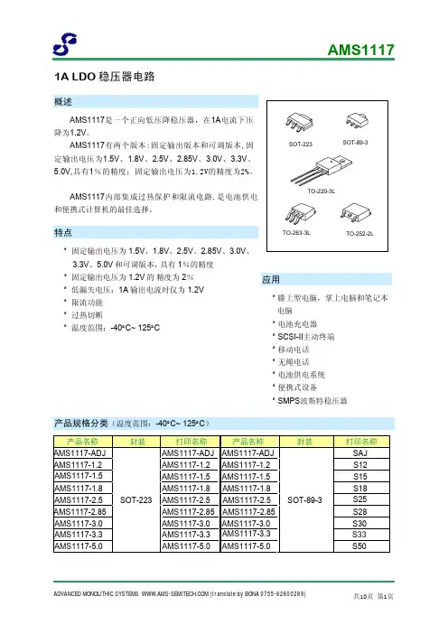
封装 SOT-223
打印名称
产品名称
AMS1117-ADJ AMS1117-1.2 AMS1117-1.5 AMS1117-1.8 AMS1117-2.5 AMS1117-2.85 AMS1117-3.0 AMS1117-3.3 AMS1117-5.0
AMS1117-ADJ AMS1117-1.2 AMS1117-1.5 AMS1117-1.8 AMS1117-2.5 AMS1117-2.85 AMS1117-3.0 AMS1117-3.3 AMS1117-5.0
封装 TO-252-2L TO-263-3L
打印名称
AMS1117-ADJ AMS1117-1.2 AMS1117-1.5 AMS1117-1.8 AMS1117-2.5 AMS1117-2.85 AMS1117-3.0 AMS1117-3.3 AMS1117-5.0 AMS1117-2.85 AMS1117-3.0 AMS1117-3.3 AMS1117-5.0
AMS1117内部集成过热保护和限流电路,是电池供电 和便携式计算机的最佳选择。
SOT-223
SOT-89-3
TO-220-3L
特点
TO-263-3L
TO-252-2L
* 固定输出电压为 1.5V、1.8V、2.5V、2.85V、3.0V、 3.3V、5.0V 和可调版本,具有 1%的精度
* 固定输出电压为 1.2V 的 精度为 2% * 低漏失电压:1A 输出电流时仅为 1.2V * 限流功能 * 过热切断 * 温度范围:-40°C~ 125°C
V
0≤IOUT≤1A, 4.25V≤VIN ≤10V
2.790 2.850 2.910
0≤IOUT≤500mA, VIN =4.10V
lm1117有几个管脚- 芯片LM1117的功能
lm1117有几个管脚? 芯片LM1117的功能
本文主要是关于lm1117的相关介绍,并着重对lm1117的管脚及其功能进行了详尽的阐述。
LM1117概述
LM1117提供电流限制和热保护。
电路包含1个齐纳调节的带隙参考电压以确保输出电压的精度在±1%以内。
LM1117系列具有LLP、TO-263、SOT-223、TO-220和TO-252 D-PAK 封装。
输出端需要一个至少10uF的钽电容来改善瞬态响应和稳定性。
替换型号
X1117是IC网络超市自主的品牌,可以很好的替换LM1117。
X1117是一款正电压输出的低压降三端线性稳压电路,在1A输出电流下的压降为1.2V。
分为两个版本,固定电压输出版本和可调电压输出版本。
固定输出电压1.5V、1.8V、2.5V、3.3V、5.0V和可调版本的电压精度为1%;固定电压为1.2V的产品输出电压精度为2%。
内部集成过热保护和限流电路,适用于各类电子产品。
A1117是台湾亿光研发生产的高效率低压降三端线性稳压器,A1117提供电流限制和热保护,以确保芯片和功率稳定性系统。
而在芯片上保证输出电压精度在±2%。
同时也提供了固定电压输出版本和可调电压输出版本,可调版本能输出从1.25V到13.8V。
其他
特性
提供1.8V、2.5V、2.85V、3.3V、5V和可调电压的型号
节省空间的SOT-223和LLP封装
电流限制和热保护功能
输出电流可达800mA
线性调整率:0.2% (Max)
负载调整率:0.4% (Max)
温度范围。
LD1117调压和固定低落电压电源器件数据手册说明书
LD1117DT33CTR LD1117S50CTR LD1117STR LD1117S33TRThis is information on a product in full production.February 2020DocID2572 Rev 371/46LD1117Adjustable and fixed low drop positive voltage regulatorDatasheet - production dataFeatures•Low dropout voltage (1 V typ.)• 2.85 V device performances are suitable for SCSI-2 active termination •Output current up to 800 mA•Fixed output voltage of: 1.2 V, 1.8 V, 2.5 V, 3.3V, 5.0 V •Adjustable version availability (V REF = 1.25 V)•Internal current and thermal limit•Available in ± 1 % (at 25 °C) and 2 % in full temperature range •Supply voltage rejection: 75 dB (typ.)DescriptionThe LD1117 is a low drop voltage regulator able to provide up to 800 mA of output current, available even in adjustable version(V REF =1.25V). Concerning fixed versions, are offered the following output voltages: 1.2 V, 1.8 V, 2.5 V, 2.85 V, 3.3 V and 5.0 V. The device is supplied in: SOT-223, DPAK, SO-8 and TO-220. The SOT-223 and DPAK surface mount packages optimize the thermal characteristics even offering a relevant space saving effect. High efficiency is assured by NPN pass transistor. In fact in this case, unlike than PNP one, the quiescent current flows mostly into the load. Only a very common 10 µF minimum capacitor is needed for stability. On chip trimming allows the regulator to reach a very tight output voltage tolerance, within ± 1 % at 25 °C. The adjustable LD1117 is pin to pin compatible with the other standard. Adjustable voltage regulators maintaining the better performances in terms of drop and tolerance.Contents LD11172/46DocID2572 Rev 37Contents1Diagram . . . . . . . . . . . . . . . . . . . . . . . . . . . . . . . . . . . . . . . . . . . . . . . . . . . 5 2Pin configuration . . . . . . . . . . . . . . . . . . . . . . . . . . . . . . . . . . . . . . . . . . . 6 3Maximum ratings . . . . . . . . . . . . . . . . . . . . . . . . . . . . . . . . . . . . . . . . . . . . 7 4Schematic application . . . . . . . . . . . . . . . . . . . . . . . . . . . . . . . . . . . . . . . 8 5Electrical characteristics . . . . . . . . . . . . . . . . . . . . . . . . . . . . . . . . . . . . . 9 6Typical application . . . . . . . . . . . . . . . . . . . . . . . . . . . . . . . . . . . . . . . . . 21 7LD1117 adjustable: application note . . . . . . . . . . . . . . . . . . . . . . . . . . . 24 8Package information . . . . . . . . . . . . . . . . . . . . . . . . . . . . . . . . . . . . . . . . 25 9Packaging mechanical data . . . . . . . . . . . . . . . . . . . . . . . . . . . . . . . . . . 38 10Order codes . . . . . . . . . . . . . . . . . . . . . . . . . . . . . . . . . . . . . . . . . . . . . . . 44 11Revision history . . . . . . . . . . . . . . . . . . . . . . . . . . . . . . . . . . . . . . . . . . . 45DocID2572 Rev 373/46LD1117List of tablesList of tablesTable 1.Absolute maximum ratings . . . . . . . . . . . . . . . . . . . . . . . . . . . . . . . . . . . . . . . . . . . . . . . . . . 7Table 2.Thermal data. . . . . . . . . . . . . . . . . . . . . . . . . . . . . . . . . . . . . . . . . . . . . . . . . . . . . . . . . . . . . 7Table 3.Electrical characteristics of LD1117#12 . . . . . . . . . . . . . . . . . . . . . . . . . . . . . . . . . . . . . . . . 9Table 4.Electrical characteristics of LD1117#18 . . . . . . . . . . . . . . . . . . . . . . . . . . . . . . . . . . . . . . . 10Table 5.Electrical characteristics of LD1117#25 . . . . . . . . . . . . . . . . . . . . . . . . . . . . . . . . . . . . . . . 11Table 6.Electrical characteristics of LD1117#33 . . . . . . . . . . . . . . . . . . . . . . . . . . . . . . . . . . . . . . . 12Table 7.Electrical characteristics of LD1117#50 . . . . . . . . . . . . . . . . . . . . . . . . . . . . . . . . . . . . . . . 13Table 8.Electrical characteristics of LD1117 (adjustable) . . . . . . . . . . . . . . . . . . . . . . . . . . . . . . . . 14Table 9.Electrical characteristics of LD1117#12C. . . . . . . . . . . . . . . . . . . . . . . . . . . . . . . . . . . . . . 15Table 10.Electrical characteristics of LD1117#18C. . . . . . . . . . . . . . . . . . . . . . . . . . . . . . . . . . . . . . 16Table 11.Electrical characteristics of LD1117#25C. . . . . . . . . . . . . . . . . . . . . . . . . . . . . . . . . . . . . . 17Table 12.Electrical characteristics of LD1117#33C. . . . . . . . . . . . . . . . . . . . . . . . . . . . . . . . . . . . . . 18Table 13.Electrical characteristics of LD1117#50C. . . . . . . . . . . . . . . . . . . . . . . . . . . . . . . . . . . . . . 19Table 14.Electrical characteristics of LD1117C (adjustable). . . . . . . . . . . . . . . . . . . . . . . . . . . . . . . 20Table 15.TO-220 mechanical data (type STD-ST Dual Gauge) . . . . . . . . . . . . . . . . . . . . . . . . . . . . 25Table 16.TO-220 mechanical data (type STD-ST Single Gauge) . . . . . . . . . . . . . . . . . . . . . . . . . . . 27Table 17.SOT-223 mechanical data . . . . . . . . . . . . . . . . . . . . . . . . . . . . . . . . . . . . . . . . . . . . . . . . . 29Table 18.SO-8 mechanical data . . . . . . . . . . . . . . . . . . . . . . . . . . . . . . . . . . . . . . . . . . . . . . . . . . . . 30Table 19.DPAK (TO-252) mechanical data (type A) . . . . . . . . . . . . . . . . . . . . . . . . . . . . . . . . . . . . . 31Table 20.DPAK (TO-252) mechanical data (type E) . . . . . . . . . . . . . . . . . . . . . . . . . . . . . . . . . . . . . 33Table 21.DPAK (TO-252) mechanical data type I . . . . . . . . . . . . . . . . . . . . . . . . . . . . . . . . . . . . . . . 35Table 22.Footprint data . . . . . . . . . . . . . . . . . . . . . . . . . . . . . . . . . . . . . . . . . . . . . . . . . . . . . . . . . . . 37Table 23.SOT-223 tape and reel mechanical data . . . . . . . . . . . . . . . . . . . . . . . . . . . . . . . . . . . . . . 39Table 24.SO-8 tape and reel mechanical data . . . . . . . . . . . . . . . . . . . . . . . . . . . . . . . . . . . . . . . . . 41Table 25.DPAK tape and reel mechanical data. . . . . . . . . . . . . . . . . . . . . . . . . . . . . . . . . . . . . . . . . 42Table 26.Order codes . . . . . . . . . . . . . . . . . . . . . . . . . . . . . . . . . . . . . . . . . . . . . . . . . . . . . . . . . . . . 44Table 27.Document revision history . . . . . . . . . . . . . . . . . . . . . . . . . . . . . . . . . . . . . . . . . . . . . . . . . 45List of figures LD11174/46DocID2572 Rev 37List of figuresFigure 1.Block diagram. . . . . . . . . . . . . . . . . . . . . . . . . . . . . . . . . . . . . . . . . . . . . . . . . . . . . . . . . . . . 5 Figure 2.Pin connections (top view) . . . . . . . . . . . . . . . . . . . . . . . . . . . . . . . . . . . . . . . . . . . . . . . . . . 6 Figure 3.Application circuit (for 1.2 V). . . . . . . . . . . . . . . . . . . . . . . . . . . . . . . . . . . . . . . . . . . . . . . . . 8 Figure 4.Application circuit (for other fixed output voltages). . . . . . . . . . . . . . . . . . . . . . . . . . . . . . . . 8 Figure 5.Negative supply . . . . . . . . . . . . . . . . . . . . . . . . . . . . . . . . . . . . . . . . . . . . . . . . . . . . . . . . . 21 Figure 6.Circuit for increasing output voltage. . . . . . . . . . . . . . . . . . . . . . . . . . . . . . . . . . . . . . . . . . 21 Figure 7.Voltage regulator with reference. . . . . . . . . . . . . . . . . . . . . . . . . . . . . . . . . . . . . . . . . . . . . 21 Figure 8.Battery backed-up regulated supply. . . . . . . . . . . . . . . . . . . . . . . . . . . . . . . . . . . . . . . . . . 22 Figure 9.Post-regulated dual supply. . . . . . . . . . . . . . . . . . . . . . . . . . . . . . . . . . . . . . . . . . . . . . . . . 23 Figure 10.Adjustable output voltage application. . . . . . . . . . . . . . . . . . . . . . . . . . . . . . . . . . . . . . . . . 24 Figure 11.Adjustable output voltage application with improved ripple rejection . . . . . . . . . . . . . . . . . 24 Figure 12.Drawing dimension TO-220 (type STD-ST Dual Gauge) . . . . . . . . . . . . . . . . . . . . . . . . . . 26 Figure 13.Drawing dimension TO-220 (type STD-ST Single Gauge). . . . . . . . . . . . . . . . . . . . . . . . . 28 Figure 14.Drawing dimension SOT-223 . . . . . . . . . . . . . . . . . . . . . . . . . . . . . . . . . . . . . . . . . . . . . . . 29 Figure 15.Drawing dimension SO-8 . . . . . . . . . . . . . . . . . . . . . . . . . . . . . . . . . . . . . . . . . . . . . . . . . . 30 Figure 16.DPAK (TO-252) package outline A. . . . . . . . . . . . . . . . . . . . . . . . . . . . . . . . . . . . . . . . . . . 32 Figure 17.DPAK (TO-252) package outline E. . . . . . . . . . . . . . . . . . . . . . . . . . . . . . . . . . . . . . . . . . . 34 Figure 18.DPAK (TO-252) package outline I . . . . . . . . . . . . . . . . . . . . . . . . . . . . . . . . . . . . . . . . . . . 36 Figure 19.DPAK footprint recommended data . . . . . . . . . . . . . . . . . . . . . . . . . . . . . . . . . . . . . . . . . . 37 Figure 20.Drawing dimension tube for TO-220 Dual Gauge (mm.) . . . . . . . . . . . . . . . . . . . . . . . . . . 38 Figure 21.Drawing dimension tube for TO-220 Single Gauge (mm.) . . . . . . . . . . . . . . . . . . . . . . . . . 38 Figure 22.Tape for SOT-223 (dimensions are in mm) . . . . . . . . . . . . . . . . . . . . . . . . . . . . . . . . . . . . 39 Figure 23.Reel for SOT-223 (dimensions are in mm). . . . . . . . . . . . . . . . . . . . . . . . . . . . . . . . . . . . . 40 Figure 24.SO-8 tape and reel dimensions . . . . . . . . . . . . . . . . . . . . . . . . . . . . . . . . . . . . . . . . . . . . . 41 Figure 25.Tape for DPAK . . . . . . . . . . . . . . . . . . . . . . . . . . . . . . . . . . . . . . . . . . . . . . . . . . . . . . . . . . 43 Figure 26.Reel for DPAK . . . . . . . . . . . . . . . . . . . . . . . . . . . . . . . . . . . . . . . . . . . . . . . . . . . . . . . . . . 43DocID2572 Rev 375/46LD1117Diagram1DiagramPin configuration LD11176/46DocID2572 Rev 372 Pin configuration Note:The TAB is connected to the V OUT.DocID2572 Rev 377/46LD1117Maximum ratings3 Maximum ratingsTable 1. Absolute maximum ratingsSymbol ParameterValue Unit V IN (1)1.Absolute maximum rating of V IN = 18 V, when I OUT is lower than 20 mA.DC input voltage 15V P TOT Power dissipation12W T STG Storage temperature range-40 to +150°C T OPOperating junction temperature rangefor C version -40 to +125°C for standard version0 to +125°CTable 2. Thermal dataSymbol ParameterSOT-223SO-8DPAK TO-220Unit R thJC Thermal resistance junction-case 152085°C/W R thJAThermal resistance junction-ambient1105510050°C/WSchematic application LD11178/46DocID2572 Rev 374 Schematic applicationDocID2572 Rev 379/46LD1117Electrical characteristics5 Electrical characteristicsRefer to the test circuits, T J = 0 to 125 °C, C O = 10 µF, R = 120 Ω between GND and OUT pins, unless otherwise specified.Table 3. Electrical characteristics of LD1117#12Symbol ParameterTest conditionMin.Typ.Max.Unit V O Output voltage V in = 3.2 V, I O = 10 mA, T J = 25 °C 1.188 1.20 1.212V V O Output voltage I O = 10 to 800 mA V in - V O = 1.4 to 10 V1.1401.20 1.260V ∆V O Line regulation V in - V O = 1.5 to 13.75 V, I O = 10 mA 0.0350.2%∆V O Load regulation V in - V O = 3 V, I O = 10 to 800 mA 0.10.4%∆V O Temperature stability 0.5%∆V O Long term stability 1000 hrs, T J = 125 °C 0.3%V in Operating input voltage 15V I adj Adjustment pin current V in ≤ 15 V60120µA ∆I adj Adjustment pin current change V in - V O = 1.4 to 10 V I O = 10 to 800 mA 15µA I O(min)Minimum load current V in = 15 V25mA I O Output current V in - V O = 5 V, T J = 25 °C 8009501300mA eN Output noise (%V O ) B = 10 Hz to 10 kHz, T J = 25 °C 0.003%SVRSupply voltage rejectionI O = 40 mA, f = 120 Hz, T J = 25 °C V in - V O = 3 V, V ripple = 1 V PP 6075dBV dDropout voltageI O = 100 mA 1 1.1VI O = 500 mA 1.05 1.15I O = 800 mA1.10 1.2Thermal regulationT a = 25 °C, 30 ms Pulse0.010.1%/W10/46DocID2572 Rev 37Refer to the test circuits, T J = 0 to 125 °C, C O = 10 µF, unless otherwise specified.Table 4. Electrical characteristics of LD1117#18Symbol Parameter Test condition Min.Typ.Max.Unit V O Output voltage V in = 3.8 V, I O = 10 mA, T J = 25 °C 1.78 1.8 1.82V V O Output voltage I O = 0 to 800 mA, V in = 3.3 to 8 V 1.76 1.84V ∆V O Line regulation V in = 3.3 to 8 V, I O = 0 mA16mV ∆V O Load regulation V in = 3.3 V, I O = 0 to 800 mA110mV ∆V O Temperature stability0.5%∆V O Long term stability1000 hrs, T J = 125 °C0.3% V in Operating input voltage I O = 100 mA15VI d Quiescent current V in≤ 8 V510mAI O Output current V in = 6.8 V, T J = 25 °C8009501300mAeN Output noise voltage B = 10 Hz to 10 kHz, T J = 25 °C100µVSVR Supply voltage rejection I O = 40 mA, f = 120 Hz, T J = 25 °CV in = 5.5 V, V ripple = 1 V PP6075dBV d Dropout voltage I O = 100 mA1 1.1V I O = 500 mA 1.05 1.15I O = 800 mA 1.10 1.2Thermal regulation T a = 25 °C, 30 ms Pulse0.010.1%/WDocID2572 Rev 3711/46Refer to the test circuits, T J = 0 to 125 °C, C O = 10 µF, unless otherwise specified.Table 5. Electrical characteristics of LD1117#25Symbol ParameterTest conditionMin.Typ.Max.Unit V O Output voltage V in = 4.5 V, I O = 10 mA, T J = 25 °C 2.475 2.52.525V V O Output voltage I O = 0 to 800 mA, V in =3.9 to 10 V 2.452.55V ∆V O Line regulation V in =3.9 to 10 V, I O = 0 mA 16mV ∆V O Load regulation V in = 3.9 V, I O = 0 to 800 mA 110mV ∆V O Temperature stability 0.5%∆V O Long term stability 1000 hrs, T J = 125 °C 0.3%V in Operating input voltage I O = 100 mA 15V I d Quiescent current V in ≤ 10 V510mA I O Output current V in = 7.5 V T J = 25 °C8009501300mA eN Output noise voltage B = 10 Hz to 10 kHz, T J = 25 °C 100µV SVRSupply voltage rejectionI O = 40 mA, f = 120 Hz, T J = 25 °C V in = 5.5 V, V ripple = 1 V PP 6075dBV dDropout voltageI O = 100 mA 1 1.1VI O = 500 mA 1.05 1.15I O = 800 mA1.10 1.2Thermal regulationT a = 25 °C, 30 ms Pulse0.010.1%/W12/46DocID2572 Rev 37Refer to the test circuits, T J = 0 to 125 °C, C O = 10 µF, unless otherwise specified.Table 6. Electrical characteristics of LD1117#33Symbol Parameter Test condition Min.Typ.Max.Unit V O Output voltage V in = 5.3 V, I O = 10 mA, T J = 25 °C 3.267 3.3 3.333V V O Output voltage I O = 0 to 800 mA, V in = 4.75 to 10 V 3.235 3.365V ∆V O Line regulation V in = 4.75 to 15 V, I O = 0 mA16mV ∆V O Load regulation V in = 4.75 V, I O = 0 to 800 mA110mV ∆V O Temperature stability0.5%∆V O Long term stability1000 hrs, T J = 125 °C0.3% V in Operating input voltage I O = 100 mA15VI d Quiescent current V in≤ 15 V510mAI O Output current V in = 8.3 V, T J = 25 °C8009501300mAeN Output noise voltage B = 10 Hz to 10 kHz, T J = 25 °C100µVSVR Supply voltage rejection I O = 40 mA, f = 120 Hz, T J = 25 °CV in = 6.3 V, V ripple = 1 V PP6075dBV d Dropout voltage I O = 100 mA1 1.1V I O = 500 mA 1.05 1.15I O = 800 mA 1.10 1.2Thermal regulation T a = 25 °C, 30 ms Pulse0.010.1%/WDocID2572 Rev 3713/46Refer to the test circuits, T J = 0 to 125 °C, C O = 10 µF, unless otherwise specified.Table 7. Electrical characteristics of LD1117#50Symbol ParameterTest conditionMin.Typ.Max.Unit V O Output voltage V in = 7 V, I O = 10 mA, T J = 25 °C 4.9555.05V V O Output voltage I O = 0 to 800 mA, V in =6.5 to 15 V 4.95.1V ∆V O Line regulation V in =6.5 to 15 V, I O = 0 mA 110mV ∆V O Load regulation V in = 6.5 V, I O = 0 to 800 mA 115mV ∆V O Temperature stability 0.5%∆V O Long term stability 1000 hrs, T J = 125 °C 0.3%V in Operating input voltage I O = 100 mA 15V I d Quiescent current V in ≤ 15 V510mA I O Output current V in = 10 V, T J = 25 °C8009501300mA eN Output noise voltage B = 10 Hz to 10 kHz, T J = 25 °C 100µV SVRSupply voltage rejectionI O = 40 mA, f = 120 Hz, T J = 25 °C V in = 8 V, V ripple = 1 V PP 6075dBV dDropout voltageI O = 100 mA 1 1.1VI O = 500 mA 1.05 1.15I O = 800 mA1.10 1.2Thermal regulationT a = 25 °C, 30 ms Pulse0.010.1%/W14/46DocID2572 Rev 37Refer to the test circuits, T J = 0 to 125 °C, C O = 10 µF, unless otherwise specified.Table 8. Electrical characteristics of LD1117 (adjustable)Symbol Parameter Test condition Min.Typ.Max.Unit V ref Reference voltage V in - V O = 2 V, I O = 10 mA, T J = 25 °C 1.238 1.25 1.262V V ref Reference voltage I O = 10 to 800 mA, V in - V O = 1.4 to 10 V 1.225 1.275V ∆V O Line regulation V in - V O = 1.5 to 13.75 V, I O = 10 mA0.0350.2%∆V O Load regulation V in - V O = 3 V, I O = 10 to 800 mA0.10.4%∆V O Temperature stability0.5%∆V O Long term stability1000 hrs, T J = 125 °C0.3% V in Operating input voltage15VI adj Adjustment pin current V in≤ 15 V60120µA ∆I adj Adjustment pin current change V in - V O = 1.4 to 10 V, I O = 10 to 800 mA15µA I O(min)Minimum load current V in = 15 V25mAI O Output current V in - V O = 5 V, T J = 25 °C8009501300mAeN Output noise (%V O) B = 10 Hz to 10 kHz, T J = 25 °C0.003%SVR Supply voltage rejection I O = 40 mA, f = 120 Hz, T J = 25 °CV in - V O = 3 V, V ripple = 1 V PP6075dBV d Dropout voltage I O = 100 mA1 1.1V I O = 500 mA 1.05 1.15I O = 800 mA 1.10 1.2Thermal regulation T a = 25 °C, 30 ms Pulse0.010.1%/WDocID2572 Rev 3715/46Refer to the test circuits, T J = -40 to 125 °C, C O = 10 µF, R = 120 Ω between GND and OUT pins, unless otherwise specified.Table 9. Electrical characteristics of LD1117#12CSymbol ParameterTest conditionMin.Typ.Max.Unit V O Output voltage V in - V O = 2 V, I O = 10 mA, T J = 25 °C 1.176 1.20 1.224V V O Output voltage I O = 10 to 800 mA, V in - V O = 1.4 to 10 V 1.1201.201.280V ∆V O Line regulation V in - V O = 1.5 to 13.75 V, I O = 10 mA 1%∆V O Load regulation V in - V O = 3 V, I O = 10 to 800 mA1%∆V O Temperature stability 0.5%∆V O Long term stability 1000 hrs, T J = 125 °C 0.3%V in Operating input voltage 15V I adj Adjustment pin current V in ≤ 15 V60120µA ∆I adj Adjustment pin current changeV in - V O = 1.4 to 10 V I O = 10 to 800 mA 15µA I O(min)Minimum load current V in = 15 V25mA I O Output current V in - V O = 5 V, T J = 25 °C 8009501300mA eN Output noise (%V O ) B = 10 Hz to 10 kHz, T J = 25 °C 0.003%SVRSupply voltage rejectionI O = 40 mA, f = 120 Hz, T J = 25 °C V in - V O = 3 V, V ripple = 1 V PP 6075dBV dDropout voltageI O = 100 mA, T J = 0 to 125 °C 1 1.1VI O = 500 mA, T J = 0 to 125 °C 1.05 1.2I O = 800 mA, T J = 0 to 125 °C 1.10 1.3Thermal regulationT a = 25 °C, 30 ms Pulse0.010.1%/W16/46DocID2572 Rev 37Refer to the test circuits, T J = -40 to 125 °C, C O = 10 µF, unless otherwise specified.Table 10. Electrical characteristics of LD1117#18CSymbol Parameter Test condition Min.Typ.Max.Unit V O Output voltage V in = 3.8 V, I O = 10 mA, T J = 25 °C 1.76 1.8 1.84V V O Output voltage I O = 0 to 800 mA, V in = 3.9 to 10 V 1.73 1.87V ∆V O Line regulation V in = 3.3 to 8 V, I O = 0 mA130mV ∆V O Load regulation V in = 3.3 V, I O = 0 to 800 mA130mV ∆V O Temperature stability0.5%∆V O Long term stability1000 hrs, T J = 125 °C0.3% V in Operating input voltage I O = 100 mA15VI d Quiescent current V in≤ 8 V510mAI O Output current V in = 6.8 V T J = 25 °C8009501300mAeN Output noise voltage B = 10 Hz to 10 kHz, T J = 25 °C100µVSVR Supply voltage rejection I O = 40 mA, f = 120 Hz, T J = 25 °CV in = 5.5 V, V ripple = 1 V PP6075dBV d Dropout voltage I O = 100 mA, T J = 0 to 125 °C1 1.1V I O = 500 mA, T J = 0 to 125 °C 1.05 1.15I O = 800 mA, T J = 0 to 125 °C 1.10 1.2V d Dropout voltage I O = 100 mA 1.1V I O = 500 mA 1.2I O = 800 mA 1.3Thermal regulation T a = 25 °C, 30 ms Pulse0.010.1%/WDocID2572 Rev 3717/46Refer to the test circuits, T J = -40 to 125 °C, C O = 10 µF, unless otherwise specified.Table 11. Electrical characteristics of LD1117#25CSymbol ParameterTest conditionMin.Typ.Max.Unit V O Output voltage V in = 4.5 V, I O = 10 mA, T J = 25 °C 2.45 2.52.55V V O Output voltage I O = 0 to 800 mA, V in =3.9 to 10 V 2.42.6V ∆V O Line regulation V in =3.9 to 10 V, I O = 0 mA 130mV ∆V O Load regulation V in = 3.9 V, I O = 0 to 800 mA 130mV ∆V O Temperature stability 0.5%∆V O Long term stability 1000 hrs, T J = 125 °C 0.3%V in Operating input voltage I O = 100 mA 15V I d Quiescent current V in ≤ 10 V510mA I O Output current V in = 7.5 V T J = 25 °C8009501300mA eN Output noise voltage B = 10 Hz to 10 kHz, T J = 25 °C 100µV SVRSupply voltage rejectionI O = 40 mA, f = 120 Hz, T J = 25 °C V in = 5.5 V, V ripple = 1 V PP 6075dBV dDropout voltageI O = 100 mA, T J = 0 to 125 °C 1 1.1VI O = 500 mA, T J = 0 to 125 °C 1.05 1.15I O = 800 mA, T J = 0 to 125 °C 1.101.2V dDropout voltageI O = 100 mA1.1V I O = 500 mA 1.2I O = 800 mA1.3Thermal regulationT a = 25 °C, 30 ms Pulse0.010.1%/W18/46DocID2572 Rev 37Refer to the test circuits, T J = -40 to 125 °C, C O = 10 µF, unless otherwise specified.Table 12. Electrical characteristics of LD1117#33CSymbol Parameter Test condition Min.Typ.Max.Unit V O Output voltage V in = 5.3 V, I O = 10 mA, T J = 25 °C 3.24 3.3 3.36V V O Output voltage I O = 0 to 800 mA, V in = 4.75 to 10 V 3.16 3.44V ∆V O Line regulation V in = 4.75 to 15 V, I O = 0 mA130mV ∆V O Load regulation V in = 4.75 V, I O = 0 to 800 mA130mV ∆V O Temperature stability0.5%∆V O Long term stability1000 hrs, T J = 125 °C0.3% V in Operating input voltage I O = 100 mA15VI d Quiescent current V in≤ 15 V510mAI O Output current V in = 8.3 V, T J = 25 °C8009501300mAeN Output noise voltage B = 10 Hz to 10 kHz, T J = 25 °C100µVSVR Supply voltage rejection I O = 40 mA, f = 120 Hz, T J = 25 °CV in = 6.3 V, V ripple = 1 V PP6075dBV d Dropout voltage I O = 100 mA, T J = 0 to 125 °C1 1.1V I O = 500 mA, T J = 0 to 125 °C 1.05 1.15I O = 800 mA, T J = 0 to 125 °C 1.10 1.2V d Dropout voltage I O = 100 mA 1.1V I O = 500 mA 1.2I O = 800 mA 1.3Thermal regulation T a = 25 °C, 30 ms Pulse0.010.1%/WDocID2572 Rev 3719/46Refer to the test circuits, T J = -40 to 125 °C, C O = 10 µF, unless otherwise specified.Table 13. Electrical characteristics of LD1117#50CSymbol ParameterTest conditionMin.Typ.Max.Unit V O Output voltage V in = 7 V, I O = 10 mA, T J = 25 °C 4.955.1V V O Output voltage I O = 0 to 800 mA, V in =6.5 to 15 V 4.85.2V ∆V O Line regulation V in =6.5 to 15 V, I O = 0 mA 150mV ∆V O Load regulation V in = 6.5 V, I O = 0 to 800 mA 150mV ∆V O Temperature stability 0.5%∆V O Long term stability 1000 hrs, T J = 125 °C 0.3%V in Operating input voltage I O = 100 mA 15V I d Quiescent current V in ≤ 15 V510mA I O Output current V in = 10 V, T J = 25 °C8009501300mA eN Output noise voltage B = 10 Hz to 10 kHz, T J = 25 °C 100µV SVRSupply voltage rejectionI O = 40 mA, f = 120 Hz, T J = 25 °C V in = 8 V, V ripple = 1 V PP 6075dBV dDropout voltageI O = 100 mA, T J = 0 to 125 °C 1 1.1VI O = 500 mA, T J = 0 to 125 °C 1.05 1.15I O = 800 mA, T J = 0 to 125 °C 1.101.2V dDropout voltageI O = 100 mA1.1V I O = 500 mA 1.2I O = 800 mA1.3Thermal regulationT a = 25 °C, 30 ms Pulse0.010.1%/WElectrical characteristics LD111720/46DocID2572 Rev 37Refer to the test circuits, T J = -40 to 125 °C, C O = 10 µF, unless otherwise specified.Table 14. Electrical characteristics of LD1117C (adjustable)Symbol Parameter Test condition Min.Typ.Max.Unit V ref Reference voltage V in - V O = 2 V, I O = 10 mA, T J = 25 °C 1.225 1.25 1.275V V ref Reference voltage I O = 10 to 800 mA, V in - V O= 1.4 to 10 V 1.2 1.3V ∆V O Line regulation V in - V O = 1.5 to 13.75 V, I O = 10 mA1%∆V O Load regulation V in - V O = 3 V, I O = 10 to 800 mA1%∆V O Temperature stability0.5%∆V O Long term stability1000 hrs, T J = 125 °C0.3% V in Operating input voltage15VI adj Adjustment pin current V in≤ 15 V60120µA ∆I adj Adjustment pin current change V in - V O = 1.4 to 10 V, I O = 10 to 800 mA110µA I O(min)Minimum load current V in = 15 V25mAI O Output current V in - V O = 5 V, T J = 25 °C8009501300mAeN Output noise (%V O) B = 10 Hz to 10 kHz, T J = 25 °C0.003%SVR Supply voltage rejection I O = 40 mA, f = 120 Hz, T J = 25 °CV in - V O = 3 V, V ripple = 1 V PP6075dBV d Dropout voltage I O = 100 mA, T J = 0 to 125 °C1 1.1V I O = 500 mA, T J = 0 to 125 °C 1.05 1.15I O = 800 mA, T J = 0 to 125 °C 1.10 1.2V d Dropout voltage I O = 100 mA 1.1V I O = 500 mA 1.2I O = 800 mA 1.3Thermal regulation T a = 25 °C, 30 ms Pulse0.010.1%/WDocID2572 Rev 3721/46LD1117Typical application6Typical applicationTypical application LD111722/46DocID2572 Rev 37DocID2572 Rev 3723/46LD1117Typical applicationLD1117 adjustable: application note LD111724/46DocID2572 Rev 377 LD1117 adjustable: application noteThe LD1117 adjustable has a thermal stabilized 1.25 ± 0.012 V reference voltage betweenthe OUT and ADJ pins. I ADJ is 60 µA typ. (120 µA max.) and ∆I ADJ is 1 µA typ. (5 µA max.).R1 is normally fixed to 120 Ω. From Figure9 we obtain:V OUT = V REF + R2 (I ADJ +I R1) = V REF + R2 (I ADJ +V REF /R1) = V REF (1 + R2 / R1) + R2 x I ADJ.In normal application R2 value is in the range of few kΩ, so the R2 x I ADJ product could notbe considered in the V OUT calculation; then the above expression becomes:V OUT = V REF (1 + R2 / R1).In order to have the better load regulation it is important to realize a good Kelvin connectionof R1 and R2 resistors. In particular R1 connection must be realized very close to OUT andADJ pin, while R2 ground connection must be placed as near as possible to the negativeLoad pin. Ripple rejection can be improved by introducing a 10 µF electrolytic capacitorplaced in parallel to the R2 resistor (see Figure10).DocID2572 Rev 3725/46LD1117Package information8 Package informationIn order to meet environmental requirements, ST offers these devices in different grades of ECOPACK packages, depending on their level of environmental compliance. ECOPACK specifications, grade definitions and product status are available at: . ECOPACK is an ST trademark.Table 15. TO-220 mechanical data (type STD-ST Dual Gauge)Dim.mmMin.Typ.Max.A 4.40 4.60b 0.610.88b1 1.14 1.70c 0.480.70D 15.2515.75D1 1.27E 1010.40e 2.40 2.70e1 4.95 5.15F 1.23 1.32H1 6.20 6.60J1 2.40 2.72L 1314L1 3.503.93L2016.40L3028.90∅P3.75 3.85Q2.652.95Package information LD111726/46DocID2572 Rev 37DocID2572 Rev 3727/46LD1117Package informationTable 16. TO-220 mechanical data (type STD-ST Single Gauge)Dim.mmMin.Typ.Max.A 4.40 4.60b 0.610.88b1 1.14 1.70c 0.480.70D 15.2515.75E 1010.40e 2.40 2.70e1 4.95 5.15F 0.510.60H1 6.20 6.60J1 2.40 2.72L 1314L1 3.503.93L2016.40L3028.90∅P3.75 3.85Q2.652.95。
MEMORY存储芯片LM1117IMPX-ADJ中文规格书
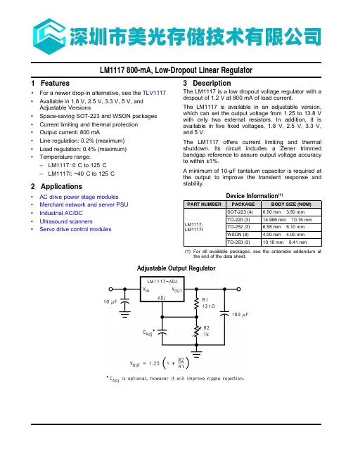
3 Description
The LM1117 is a low dropout voltage regulator with a dropout of 1.2 V at 800 mA of load current.
The LM1117 is available in an adjustable version, which can set the output voltage from 1.25 to 13.8 V with only two external resistors. In addition, it is available in five fixed voltages, 1.8 V, 2.5 V, 3.3 V, and 5 V.
(2) The maximum power dissipation is a function of TJ(max) , RθJA, and TA. The maximum allowable power dissipation at any ambient temperature is PD = (TJ(max)–TA)/RθJA. All numbers apply for packages soldered directly into a PCB.
A minimum of 10-µF tantalum capacitor is required at the output to improve the transient response and stability.
Device Information(1)
PART NUMBER PACKAGE
7.3 Recommended Operating Conditions
over operating free-air temperature range (unless otherwise noted)
LD1117中文资料详解
LD1117中文资料详解
概述:
LD1117是低开启电压稳压源。
在额定工作温度范围内,可以进行有效过温和过流保护。
应用范围广泛,可以提供1.2V,
1.5V,1.8V,
2.5V,
3.3V,5V固定电压输出;同时也提供可调输出(在1.2~~VCC),用外接2电阻调整来实现。
基本特性:
1.此稳压源输入最高电压16v
2.提供固定电压输出1.2v,1.5v,1.8v,2.5v,
3.3v,5v
3.输出电压精度可控制在1%的范围内
4.较宽输出电流范围1mA--1A
5.非常好线性调整率和负载调整率
6.低开启电压
7.提供封装SOT-223,TO-252
应用范围:
1.高效率线性电源
2.影音产品
3.仪器仪表、显示器
4.通讯产品及电池充电
5.主芯片供电
6.电脑周边及车载产品产品以下为网络资料:。
MEMORY存储芯片LM1117MPX-3.3中文规格书
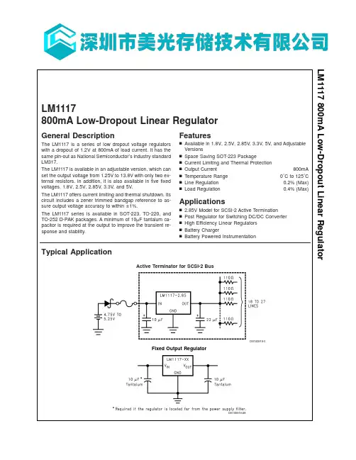
LM1117800mA Low-Dropout Linear RegulatorGeneral DescriptionThe LM1117is a series of low dropout voltage regulators with a dropout of1.2V at800mA of load current.It has the same pin-out as National Semiconductor’s industry standard LM317.The LM1117is available in an adjustable version,which can set the output voltage from1.25V to13.8V with only two ex-ternal resistors.In addition,it is also available in five fixed voltages,1.8V,2.5V,2.85V,3.3V,and5V.The LM1117offers current limiting and thermal shutdown.Its circuit includes a zener trimmed bandgap reference to as-sure output voltage accuracy to within±1%.The LM1117series is available in SOT-223,TO-220,and TO-252D-PAK packages.A minimum of10µF tantalum ca-pacitor is required at the output to improve the transient re-sponse and stability.Featuresn Available in1.8V,2.5V,2.85V,3.3V,5V,and Adjustable Versionsn Space Saving SOT-223Packagen Current Limiting and Thermal Protectionn Output Current800mA n Temperature Range0˚C to125˚C n Line Regulation0.2%(Max) n Load Regulation0.4%(Max)Applicationsn 2.85V Model for SCSI-2Active Terminationn Post Regulator for Switching DC/DC Convertern High Efficiency Linear Regulatorsn Battery Chargern Battery Powered InstrumentationTypical ApplicationActive Terminator for SCSI-2BusDS100919-5Fixed Output RegulatorDS100919-28LM1117 800mA Low-Dropout Linear RegulatorOrdering InformationPackageTemperature Range Packaging Marking Transport Media NSC Drawing 0˚C to +125˚C 3-lead SOT-223LM1117MPX-ADJN03A Tape and Reel MA04A LM1117MPX-1.8N12A Tape and Reel *LM1117MPX-2.5N13A Tape and Reel LM1117MPX-2.85N04A Tape and Reel LM1117MPX-3.3N05A Tape and Reel LM1117MPX-5.0N06A Tape and Reel 3-lead TO-220LM1117T-ADJLM1117T-ADJ Rails T03B LM1117T-2.85LM1117T-2.85Rails LM1117T-3.3LM1117T-3.3Rails LM1117T-5.0LM1117T-5.0Rails 3-lead TO-252LM1117DTX-ADJLM1117DT-ADJ Tape and Reel TD03BLM1117DTX-1.8LM1117DT-1.8Tape and Reel *LM1117DTX-2.5LM1117DT-2.5Tape and Reel LM1117DTX-2.85LM1117DT-2.85Tape and Reel LM1117DTX-3.3LM1117DT-3.3Tape and Reel LM1117DTX-5.0LM1117DT-5.0Tape and Reel Note:*Contact factory for availability.Block DiagramDS100919-1L M 1117Absolute Maximum Ratings (Note 1)If Military/Aerospace specified devices are required,please contact the National Semiconductor Sales Office/Distributors for availability and specifications.Maximum Input Voltage (V IN to GND)LM1117-ADJ,LM1117-1.8,LM1117-2.5,LM1117-3.3,LM1117-5.020V Power Dissipation (Note 2)Internally Limited Junction Temperature (T J )(Note 2)150˚C Storage Temperature Range-65˚C to 150˚C Lead Temperature TO-220(T)Package 260˚C,10sec SOT-223(IMP)Package 260˚C,4sec ESD Tolerance (Note 3)2000V Operating Ratings (Note 1)Input Voltage (V IN to GND)LM1117-ADJ,LM1117-1.8,LM1117-2.5,LM1117-3.3,LM1117-5.015V LM1117-2.8510V Junction Temperature Range (T J )(Note 2)0˚C to 125˚CElectrical CharacteristicsTypicals and limits appearing in normal type apply for T J =25˚C.Limits appearing in Boldface type apply over the entire junc-tion temperature range for operation,0˚C to 125˚C.SymbolParameter Conditions Min (Note 5)Typ (Note 4)Max (Note 5)Units V REF Reference Voltage LM1117-ADJI OUT =10mA,V IN -V OUT =2V,T J =25˚C10mA ≤I OUT ≤800mA,1.4V ≤V IN -V OUT≤10V1.2381.225 1.2501.250 1.2621.270V V V OUT Output Voltage LM1117-1.8I OUT =10mA,V IN =3.8V,T J =25˚C0≤I OUT ≤800mA,3.2V ≤V IN ≤10V1.7821.746 1.8001.800 1.8181.854V V LM1117-2.5I OUT =10mA,V IN =4.5V,T J =25˚C0≤I OUT ≤800mA,3.9V ≤V IN ≤10V2.4752.450 2.5002.500 2.5252.550V V LM1117-2.85I OUT =10mA,V IN =4.85V,T J =25˚C0≤I OUT ≤800mA,4.25V ≤V IN ≤10V0≤I OUT ≤500mA,V IN =4.10V2.8202.7902.790 2.8502.8502.850 2.8802.9102.910V V V LM1117-3.3I OUT =10mA,V IN =5V T J =25˚C0≤I OUT ≤800mA,4.75V ≤V IN ≤10V3.2673.235 3.3003.300 3.3333.365V V LM1117-5.0I OUT =10mA,V IN =7V,T J =25˚C0≤I OUT ≤800mA,6.5V ≤V IN ≤12V4.9504.9005.0005.000 5.0505.100V V ∆V OUT Line Regulation(Note 6)LM1117-ADJ I OUT =10mA,1.5V ≤V IN -V OUT ≤13.75V0.0350.2%LM1117-1.8I OUT =0mA,3.2V ≤V IN ≤10V16mV LM1117-2.5I OUT =0mA,3.9V ≤V IN ≤10V16mV LM1117-2.85I OUT =0mA,4.25V ≤V IN ≤10V16mV LM1117-3.3I OUT =0mA,4.75V ≤V IN ≤15V16mV LM1117-5.0I OUT =0mA,6.5V ≤V IN ≤15V 110mVL M 1117Typical Performance CharacteristicsDropout Voltage(V IN-V OUT)DS100919-22Short-Circuit CurrentDS100919-23Load RegulationDS100919-24LM1117-ADJ Ripple RejectionDS100919-6LM1117-ADJ Ripple Rejection vs.CurrentDS100919-7Temperature StabilityDS100919-25LM1117。
1117稳压芯片参数
1117稳压芯片参数
1117是一款稳压芯片,它的出现为电脑主机和其他外设的安全降压而提供了更有效的保护。
该产品具有采用最新的技术、高效的工作特性、高安全性。
它可以提供稳定的电压输出,并能够保持充足的供电,延长电源的寿命。
1117稳压芯片使用双分路控制系统,可以实现输入输出完全分离,确保输出稳定,有效阻止衰减造成的偏差,降低失真程度,抑制频率和他电压输出的噪声,提高电源线路的抗干扰性能。
此外,1117稳压芯片采用双稳压设计,可实现外部下调和上调电压输出,使用多种工作环境,可确保稳压功能正常运行。
1117稳压芯片的参数很多,可分为输入参数和输出参数两类。
输入参数包括:电气特性,输入电压、输入电压范围、输入电流、输入阻抗、输入电流限制、输入功耗、输入开关和保护。
输出参数包括:电气特性,输出电压、输出电压范围、输出电流、输出阻抗、输出精度、电源追踪精度、输出纹波和噪声、输出时间延迟和软启动时间。
另外,1117稳压芯片的功能特性还包括:电压温度补偿、电压调节比、回路增益、过流保护、过温过载保护、反向连接保护、功耗模式以及电路自检功能。
1117稳压芯片已成为许多电脑外设产品的主要配件,它们使用它可以实现安全降压,保护主机设备,并保证正常工作。
此外,它具有高可靠性、高效率和低功耗,是电脑使用的理想选择。
总之,1117稳压芯片的参数很多,其输入输出参数可实现安全降压,高可靠性、高效率和低功耗,可以有效保护主机和其他外设的安全。
此外,它的使用还能延长电源的寿命,进一步降低故障率,为电脑带来更多的福利。
LD1117系列各品牌技术规格书
ABSOLUTE MAXIMUM RATINGS (Note 1)
Power Dissipation
Internally limited
Input Voltage
15V
Operating Junction Temperature Range
Control Section
0°C to 125°C
Power Transistor
Adjust Pin Current Change
Temperature Stability
Long Term Stability
RMS Output Noise (% of VOUT ) Thermal Resistance Junction-to-Case
2.82
2.850
2.88
V
2.79
2.850
2.91
V
0 ≤ IOUT ≤ 800mA , 4.75V ≤ VIN ≤ 12V
3.267 3.300
3.333
V
3.235 3.300
3.365
V
0 ≤ IOUT ≤ 800mA , 6.5V ≤ VIN ≤ 12V
4.950 5.000
5.050
V
ϕ JA= 90°C/W*
* With package soldering to copper area over backside
1117稳压芯片参数
1117稳压芯片参数
稳压芯片参数是指一种半导体元件,其主要功能是提供调节和稳定的电压输出,用于维护电子系统的性能和安全的稳定运转。
这种半导体芯片是一种非常重要的元件,它可以控制和调整电路的电压,从而保证电子设备的正常运行。
1117稳压芯片是一种常用的稳压芯片,它有三种型号:
LM1117-2.5V、LM1117-3.3V和LM1117-5.0V。
它采用恒流恒压工作模式,其最大输出电流在1A左右,并且可以承受较大的负载波动。
其参数如下:
1)输出电压:2.5V,3.3V,5.0V;
2)输出电流:最大1A,最大输入电压为36V;
3)保护功能:具有短路保护和过压保护功能;
4)输出噪声:低于50μV/V;
5)开关频率:1.2MHz;
6)热型号:SOT-223、 PDIP-8或TO-251-2。
1117稳压芯片具有非常多的优势,它可以具有短路保护,热保护和过压保护功能,从而保证电路的可靠性。
它的封装和热型号也可以根据客户要求定制,使用非常方便。
此外,它还具有良好的静态性能和动态性能,因此可以很好地适应高频或工业应用环境。
1117稳压芯片的应用也非常广泛,它可以用于电脑,网络设备,电源适配器,数字家电,汽车电子和通讯设备等领域。
它可以提供稳定的电压输出,保证电子系统正常工作,可靠性更好。
综上,1117稳压芯片参数具有较高的性能,可以很好地保证电子系统的可靠性。
它的应用非常广泛,可以满足多种不同的电子设备的需求。
它的优势使它成为一种非常有价值的稳压芯片元件,也是电路设计中的一种重要元件。
MEMORY存储芯片LM1117MPX-ADJ中文规格书
10Power Supply RecommendationsThe input supply to the LM1117must be kept at a voltage level such that its maximum rating is not exceeded. The minimum dropout voltage must also be met with extra headroom when possible to keep the LM1117in regulation.An input capacitor is recommended.For more information regarding capacitor selection,refer to External Capacitors.11Layout11.1Layout GuidelinesSome layout guidelines must be followed to ensure proper regulation of the output voltage with minimum noise. Traces carrying the load current must be wide to reduce the amount of parasitic trace inductance and the feedback loop from V OUT to ADJ must be kept as short as possible.To improve PSRR,a bypass capacitor can be placed at the ADJ pin and must be located as close as possible to the IC.In cases when V IN shorts to ground, an external diode must be placed from V OUT to V IN to divert the surge current from the output capacitor and protect the IC.The diode must be placed close to the corresponding IC pins to increase their effectiveness.11.1.1Heatsink RequirementsWhen an integrated circuit operates with an appreciable current,its junction temperature is elevated.It is important to quantify its thermal limits in order to achieve acceptable performance and reliability.This limit is determined by summing the individual parts consisting of a series of temperature rises from the semiconductor junction to the operating environment.A one-dimensional steady-state model of conduction heat transfer is demonstrated in Figure22.The heat generated at the device junction flows through the die to the die attach pad, through the lead frame to the surrounding case material,to the printed circuit board,and eventually to the ambient environment.Below is a list of variables that may affect the thermal resistance and in turn the need for a heatsink.ponent and Application VariablesRθJC(COMPONENT VARIABLES)RθJA(APPLICATION VARIABLES)Leadframe Size and Material Mounting Pad Size,Material,and LocationNo.of Conduction Pins Placement of Mounting PadDie Size PCB Size and MaterialDie Attach Material Traces Length and WidthMolding Compound Size and Material Adjacent Heat SourcesVolume of AirAmbient TemperatueShape of Mounting PadThe case temperature is measured at the point where the leads contact with the mounting pad surfaceFigure22.Cross-Sectional View of Integrated Circuit Mounted on a Printed Circuit BoardPACKAGING INFORMATIONAddendum-Page 1Addendum-Page 2Device PackageType PackageDrawingPins SPQ ReelDiameter(mm)ReelWidthW1(mm)A0(mm)B0(mm)K0(mm)P1(mm)W(mm)Pin1QuadrantLM1117LD-ADJ/NOPB WSON NGN81000178.012.4 4.3 4.3 1.38.012.0Q1 LM1117LDX-1.8/NOPB WSON NGN84500330.012.4 4.3 4.3 1.38.012.0Q1 LM1117LDX-ADJ/NOPB WSON NGN84500330.012.4 4.3 4.3 1.38.012.0Q1 LM1117MP-1.8/NOPB SOT-223DCY41000330.016.47.07.5 2.212.016.0Q3 LM1117MP-2.5/NOPB SOT-223DCY41000330.016.47.07.5 2.212.016.0Q3 LM1117MP-3.3/NOPB SOT-223DCY41000330.016.47.07.5 2.212.016.0Q3 LM1117MP-5.0/NOPB SOT-223DCY41000330.016.47.07.5 2.212.016.0Q3 LM1117MP-ADJ/NOPB SOT-223DCY41000330.016.47.07.5 2.212.016.0Q3 LM1117MPX-1.8/NOPB SOT-223DCY42000330.016.47.07.5 2.212.016.0Q3 LM1117MPX-2.5/NOPB SOT-223DCY42000330.016.47.07.5 2.212.016.0Q3 LM1117MPX-3.3SOT-223DCY42000330.016.47.07.5 2.212.016.0Q3 LM1117MPX-3.3/NOPB SOT-223DCY42000330.016.47.07.5 2.212.016.0Q3 LM1117MPX-5.0/NOPB SOT-223DCY42000330.016.47.07.5 2.212.016.0Q3 LM1117MPX-ADJ/NOPB SOT-223DCY42000330.016.47.07.5 2.212.016.0Q3 LM1117SX-3.3/NOPB DDPAK/TO-263KTT3500330.024.410.7514.85 5.016.024.0Q2LM1117SX-5.0/NOPB DDPAK/TO-263KTT3500330.024.410.7514.85 5.016.024.0Q2LM1117SX-ADJ/NOPB DDPAK/TO-263KTT3500330.024.410.7514.85 5.016.024.0Q2。
- 1、下载文档前请自行甄别文档内容的完整性,平台不提供额外的编辑、内容补充、找答案等附加服务。
- 2、"仅部分预览"的文档,不可在线预览部分如存在完整性等问题,可反馈申请退款(可完整预览的文档不适用该条件!)。
- 3、如文档侵犯您的权益,请联系客服反馈,我们会尽快为您处理(人工客服工作时间:9:00-18:30)。
VIN=3V ΔVOUT LD1117 : IOUT=0 ~ 800mA
LD1117A : IOUT=0 ~ 1000mA
ΔVOUT
ΔVOUT 1000 hrs, TJ =125°C
VIN IOUT=100mA
IQ VIN≤10V
ILIMIT VIN=6.5V, TJ =25°C
LD1117 LD1117A
LD1117①L-xx-TQ3-②-③ LD1117①L-xx-S08-②-③
Note: Pin Assignment: I:VIN O:VOUT G:GND
Package
SOT-223 SOT-89 TO-220 TO-252 TO-263 TO-263-3 SOP-8
② Pin Assignment
Dropout Voltage
Thermal Regulation
SYMBOL
TEST CONDITIONS
VOUT VIN=3.5V, IOUT=10mA, TJ=25°C
VIN=3 to 8V
VOUT LD1117 : IOUT=0 ~ 800mA
LD1117A : IOUT=0 ~ 1.0A
ΔVOUT VIN=3 to 8V, IOUT=0mA
For LD1117/A-1.5 PARAMETER
Output Voltage
Output Voltagon
Temperature stability Long Term Stability Operating Input Voltage Quiescent Current Current Limit Output Noise Voltage Supply Voltage Rejection
LD1117/A
LINEAR INTEGRATED CIRCUIT
ABSOLUTE MAXIMUM RATINGS (Ta=25℃)
PARAMETER
SYMBOL
RATINGS
DC Input Voltage
VIN
18
Power Dissipation
PD
Internally limited
Junction Temperature
FEATURES
* Low dropout voltage * Suitable for SCSI-2 active termination if VOUT set to 2.85V * Output current up to 0.8A for 1117 and 1.0A for 1117A * Built-in current limit and over temperature protection * Available in ±1%(at 25°C) and 2% in all temperature range * Low current consumption
IOUT=1000 mA
Ta=25°C, 30ms Pulse
TYP. 1.200
1.200
1
1
0.5 0.3
5
2 100 75 1.00 1.15 1.20 1.20 0.01
MAX. 1.212 1.224
6 10
15 10
5
1.10 1.25 1.30 1.30 0.10
UNIT V
V
mV
mV
UNIT V
°C °C
RECOMMENDED OPERATING RATINGS
PARAMETER Input Voltage Operating Junction Temperature Range
SYMBOL VIN TJ
RATINGS 15
0 ~ +125
UNIT V °C
ELECTRICAL CHARACTERISTICS
Dropout Voltage
Thermal Regulation
IO(MIN) VIN=15V
eN B=10Hz to 10KHz, TJ =25°C
SVR IOUT=40mA, f=120Hz, TJ =25°C,
60
VIN=4.2V, VRIPPLE=1Vpp
IOUT=100mA
VD
IOUT=500mA IOUT=800mA
TJ
+150
Storage temperature
TSTG
-65 ~ +150
Note Absolute maximum ratings are those values beyond which the device could be permanently damaged.
Absolute maximum ratings are stress ratings only and functional device operation is not implied.
LD1117 LD1117A
eN SVR
B=10Hz to 10KHz, TJ =25°C IOUT=40mA, f=120Hz, TJ =25°C, VIN=5.5V, Vripple=1Vpp
Output Voltage
Line Regulation
Load Regulation
Temperature stability Long Term Stability Operating Input Voltage Quiescent Current Current Limit
VOUT
VOUT
ΔVOUT
ΔVOUT VIN=3.3 to 8V, IOUT=0mA
ΔVOUT
VIN=3.3V LD1117 : IOUT=0 ~ 800mA LD1117A : IOUT=0 ~ 1000mA
ΔVOUT ΔVOUT 1000 hrs, TJ =125°C
VIN IOUT=100mA IQ VIN≤8V
ILIMIT VIN=6.8V, TJ =25°C
2 of 12
QW-R102-006,Q
LD1117/A
BLOCK DIAGRAM
LINEAR INTEGRATED CIRCUIT
UNISONIC TECHNOLOGIES CO., LTD
3 of 12
QW-R102-006,Q
LD1117①-xx-TA3-②-③ LD1117①-xx-TN3-②-③ LD1117①-xx-TQ2-②-③
LD1117①L-xx-TA3-②-③ LD1117①L-xx-TN3-②-③ LD1117①L-xx-TQ2-②-③
LD1117①-xx-TQ3-②-③ LD1117①-xx-S08-②-③
③ Packing
A: GOI B: OGI C: GIO D: IGO
R: Tape Reel T: Tube
GOOIxOOx
Copyright © 2005 Unisonic Technologies Co., Ltd
1 of 12
QW-R102-006,Q
Note: Current code: Blank: 0.8A A: 1A
PIN CONFIGURATION
GND 1
VOUT
2
VOUT
3
VIN
4
LINEAR INTEGRATED CIRCUIT
MARKING
8 NC
7
VOUT
6 VOUT
5 NC
UNISONIC TECHNOLOGIES CO., LTD
Dropout Voltage
Thermal Regulation
SYMBOL
TEST CONDITIONS
VOUT VIN=3.8V, IOUT=10mA, TJ =25°C
VOUT
VIN=3.3 to 8V LD1117 : IOUT=0 ~ 800mA LD1117A : IOUT=0 ~ 1000mA
LD1117/A
MARKING INFORMATION
PACKAGE
VOLTAGE CODE
SOT-89
SOT-223
TO-220 TO-252 TO-263 TO-263-3
12 :1.2V 15 :1.5V 18 :1.8V 25 :2.5V 2J :2.85V 30 :3.0V 33 :3.3V 36 :3.6V 50 :5.0V AD :ADJ
ΔVOUT
ΔVOUT ΔVOUT
VIN IQ ILIMIT
VIN=3.2V, IOUT=10mA, TJ=25°C VIN=2.7 to 8V LD1117 : IOUT=0 ~ 800mA LD1117A : IOUT=0 ~ 1.0A VIN=2.7 to 8V, IOUT=0mA VIN=2.7V LD1117 : IOUT=0 ~ 800mA LD1117A : IOUT=0 ~ 1000mA
(Ta=25℃, refer to the test circuits, TJ=0 to 125°C, Co=10μF unless otherwise specified)
For LD1117/A-1.2
PARAMETER
SYMBOL
TEST CONDITIONS
MIN.
Output Voltage
% % V mA mA
mA μV dB V V V V %/W
UNISONIC TECHNOLOGIES CO., LTD
4 of 12
QW-R102-006,Q
LD1117/A
LINEAR INTEGRATED CIRCUIT
ELECTRICAL CHARACTERISTICS(Cont.)