MEMORY存储芯片STM32F103C8T6中文规格书
stm32f103c8t6的数据手册
《STM32F103C8T6的数据手册》一、概述STM32F103C8T6是ST公司生产的32位ARM Cortex-M3内核的微控制器,具有丰富的外设接口和强大的性能,广泛应用于工业控制、自动化设备、消费类电子产品等领域。
本文旨在对STM32F103C8T6的数据手册进行全面的介绍,帮助读者更好地理解和应用这款微控制器。
二、概览1. 器件简介STM32F103C8T6是一款高性能、低功耗的微控制器,拥有72MHz 工作频率,64KB Flash存储器和20KB RAM。
其丰富的外设接口包括多个通用定时器、串行通信接口、模拟-数字转换器等,适用于各种复杂的应用场景。
2. 功能特性STM32F103C8T6的主要功能特性包括:- ARM Cortex-M3内核- 64KB Flash存储器、20KB RAM- 丰富的外设接口:通用定时器、串行通信接口、模拟-数字转换器等- 低功耗模式:多种低功耗模式可选,满足不同需求3. 应用领域STM32F103C8T6广泛应用于工业控制、自动化设备、消费类电子产品等领域,如工业控制器、电源管理系统、医疗设备等。
三、详细规格1. 通用定时器STM32F103C8T6内置了多个通用定时器,可用于生成精准的定时脉冲,计数器和PWM输出等功能。
2. 串行通信接口该微控制器支持多种串行通信接口,包括SPI、I2C和USART,可用于与外部设备进行高速数据传输。
3. 模拟-数字转换器STM32F103C8T6配备了多个模拟-数字转换器,可实现精确的模拟信号采集和处理。
4. 中断控制器中断控制器可实现对各种外部事件的响应,提高系统的实时性和稳定性。
5. 时钟控制时钟控制模块支持多种时钟源和分频设置,可满足不同应用场景的时序要求。
6. 低功耗模式STM32F103C8T6支持多种低功耗模式,包括待机模式、休眠模式和停止模式,有效降低系统功耗,延长电池寿命。
7. 引脚定义STM32F103C8T6具有多种引脚,可供用户定义为输入/输出口,用于连接外部设备和传感器。
stm32f103c8t6中文手册
stm32f103c8t6中文手册STM32F103系列微处理器,STM32F103器件* * STM32F103 * * Cortex-M3内核,CPU速度为72 MHz,最大闪存为1 MB。
包括电机控制外设和USB全速接口。
STM32系列臂式Cortex-M3 32位闪存微控制器具有低功耗,低电压,出色的性能和实时功能。
包类型系列适用于您的嵌入式应用程序。
MCU体系结构具有易于使用的STM32平台,适用于包括电机驱动,PC和游戏,HVAC以及工业应用在内的应用。
32位RISC引脚对引脚软件兼容的SRAM 高达96 KB 闪存高达1MB电源:2 V至3.6 V温度范围:-40至+ 85°C或-40至+ 105°C?stm32f1系列32位臂?皮质?-M3微控制器,意法半导体的STM32闪存微控制器。
STM32系列是基于ARM cortex Gamma M3的核心突破-嵌入式应用程序特殊开发的核心。
STM32系列受益于对Cortex-M3体系结构的增强,其中包括thumb-2指令集,该指令集提供了更高的性能,更好的编码密度,更快的中断响应以及所有领先的工业功耗。
出色的实时性能,出色的效率和新的外围设备,最大限度地提高了串行引脚,外围设备和软件兼容性之间的集成Stm32f103c8t6是中密度性能线,配备了Arm Cortex-M3 32位微控制器和48通道LQFP 封装。
它结合了高性能RISC内核,72MHz的工作频率,高速嵌入式存储器,增强的I / O范围以及与两条APB总线的外部连接。
Stm32f103c8t6具有12位ADC,计时器,PWM计时器,标准和高级通信接口。
全面的省电模式使设计人员能够设计低功耗应用。
工作电压范围:2V至3.6v.64k字节闪存。
20K字节SRAM.CRC 计算单元,96位唯一ID。
两个12位,1μs ADC(最多10个通道)。
7通道DMA控制器,3个通用定时器和1个高级控制定时器。
基于STM单片机STM32F103CBT6应用方案-奥伟斯
奥伟斯科技为您提供STM单片机STM32F103CBT6应用参考设计方案●内容导航:●公司简介●STM32F103CBT6产品规格书●产品图片●优势产品简介STM32F103C8T6基于ARM的32位MCU,带闪存,USB,CAN,7个16位定时器,2个ADC和9个通信接口-奥伟斯科技STM32F103C8T6特征■内核:ARM 32位Cortex™-M3 CPU- 72 MHz,90 DMIPS,1.25 DMIPS / MHz- 单周期乘法和硬件师- 带有43的嵌套中断控制器可屏蔽中断通道- 中断处理(低至6个CPU尾部链接■回忆- 32至128 KB的闪存- 6至20 KB的SRAM■时钟,复位和电源管理- 2.0至3.6 V应用电源和I / O.- POR,PDR和可编程电压探测器(PVD)- 4至16 MHz石英振荡器- 内部8 MHz工厂调整RC- 内部32 kHz RC- 用于CPU时钟的PLL- 用于RTC的专用32 kHz振荡器校准■低功耗- 睡眠,停止和待机模式- 用于RTC和备份寄存器的VBAT电源■2 x 12位,1μsA/ D转换器(16通道)- 转换范围:0至3.6 V.- 双采样和保持功能- 可与高级控制计时器同步- 温度感应器■DMA- 7通道DMA控制器- 支持外设:定时器,ADC,SPI,I2Cs和USART■调试模式- 串行线调试(SWD)和JTAG接口■最多80个快速I / O端口- 32/49/80 5个V容错I / O.- 全部可映射16个外部中断矢量- 原子读/修改/写操作■最多7个计时器- 最多三个16位定时器,每个定时器最多4个IC / OC / PWM或脉冲计数器- 16位,6通道高级控制定时器:PWM输出最多6个通道死时间的产生和紧急情况停- 2个16位看门狗定时器(独立和窗口)- SysTick计时器:一个24位的向下计数器■最多9个通信接口- 最多2个I2C接口(SMBus / PMBus)- 最多3个USART(ISO 7816接口,LIN,IrDA功能,调制解调器控制)- 最多2个SPI(18 Mbit / s)- CAN接口(2.0B有源)- USB 2.0全速接口STM32F103系列订购型号:STM32F103C6T6 STM32F103R6T6 STM32F103C8T6 STM32F103R8T6 STM32F103V8T6STM32F103RBT6 STM32F103VBT6公司简介深圳市奥伟斯科技有限公司是一家专注触摸芯片,单片机,电源管理芯片,语音芯片,场效应管,显示驱动芯片,网络接收芯片,运算放大器,红外线接收头及其它半导体产品的研发,代理销售推广的高新技术企业.奥伟斯科技自成立以来一直致力于新半导体产品在国内的推广与销售,年销售额超过壹亿人民币是一家具有综合竞争优势的专业电子元器件代理商.本公司代理推广的一系列优秀触摸芯片及语音芯片,现以大批量应用到智能电子锁、饮水机、电饭煲、LED台灯等控制器为顾客提供最佳解决方案,受到广大客户的一致赞誉。
stm32f103c8t6中文参数

stm32f103c8t6中文参数1.简介本文档将介绍ST M32F103C8T6微控制器的中文参数。
S T M32F103C8T6是一款基于AR MC or tex-M3内核的高性能微控制器,具有丰富的外设和低功耗特性。
本文将详细介绍其主要技术参数和特性。
2.技术参数S T M32F103C8T6的主要技术参数如下:-核心:AR M32位Cor t ex-M3C PU-频率:最高工作频率为72MH z-存储器:64K BF la sh存储器,20K BR AM-时钟:内部高精度8M Hz RC振荡器,外部时钟输入支持-通信接口:2个SP I接口,3个I2C接口,2个UA RT接口,1个U S B接口-A DC:12位模数转换器,最多16个通道-P WM:16路输出-G PI O:最多37个通用I/O引脚-供电电压:3.3V3.特性3.1高性能S T M32F103C8T6的A R MC or te x-M3处理器提供高性能的计算能力和快速响应速度。
其最高工作频率为72M Hz,可以满足大部分应用的需求。
3.2丰富的外设该微控制器配备了多种外设,包括SP I、I2C、UA RT和U SB接口,可以方便地与其他设备进行通信。
同时,内部集成了12位模数转换器,可以实现精确的模拟信号采集。
3.3低功耗特性S T M32F103C8T6具备低功耗特性,可满足对功耗敏感的应用需求。
其内部集成了8MH zR C振荡器,可以有效减少功耗,并支持外部时钟输入。
3.4强大的G P I O该微控制器拥有最多37个通用I/O引脚,可以灵活地实现各种输入输出功能。
G PI O引脚具备多种工作模式和中断功能,适用于各种应用场景。
4.应用领域由于ST M32F103C8T6具备高性能、丰富的外设和低功耗特性,它在各种领域都有广泛的应用,包括但不限于:-工业自动化控制系统-智能家居系统-医疗仪器设备-汽车电子控制系统-智能电源管理系统-物联网终端设备5.总结本文对S TM32F103C8T6微控制器的中文参数进行了详细介绍。
STM32F051C8T6开发板用户手册说明书

Open051C User ManualContentsOPEN051C USER MANUAL (1)1.OVERVIEW (2)1.1.W HAT’S ON BOARD (2)2.DEMO (4)2.1.8I OS (5)2.2.ADC+DMA (5)2.3.DAC+DMA (6)2.4.GPIO_LED (7)2.5.GPIO_LED_KEY (7)2.6.I2C (7)2.7.I2S UDA1380&SD_FATFS (8)2.8.JOYSTICK (8)2.9.LCD22 (8)2.10.LCD22-T OUCH (9)2.11.FATFS V0.08A-SD C ARD (10)2.12.NRF24L01 (10)2.13.O NE-W IRE (11)2.14.PS2 (11)2.15.RTC (12)2.16.SPI (12)2.17.U COS II (13)ART (13)3.REVISION HISTORY (14)1. Overview 1.1. What’s on board[ MCU ]1. STM32F051C8T6the high performance STM32 MCU which features:Core:Cortex-M0 32-bit RISC;Operating Frequency:48MHz;Operating Voltage:2-3.6V;Package:LQFP48;I/Os: 39;Memories:64KB Flash, 8kB RAM;Communication Interfaces: 2 x SPI, 2 x USART, 2 x I2C, 1 x I2S;[ Component ]3. Power supply switch5V DC or USB4. Power indicator5. User LEDfor indicating I/O status6. Reset key7. User LEDfor I/O input and/or interact with running code 8. Joystickfive positionAD & DA converters : 1 x AD (12-bit, 1μs, shares 16 channels);Debugging/Programming : supports SWD (serial wire debug) interfaces, supports IAP2. AMS1117-3.33.3V voltage regulator[ Interface ]11. 8I/Os + DAC + ADC Interfaceeasily connects to keypad, motor, etc. 12. SPI1 / SPI2 interfaceeasily connects to SPI peripherals such as FLASH (AT45DBxx), SD card, MP3, etc.convenient for connecting AD module, thanks to the SPI1 alternative AD function 13. I2C1 / I2C2 interfaceeasily connects to I2C peripherals such as I/O expander (PCF8574), EEPROM (AT24Cxx), etc.14. LCD interfaceeasily connects to the touch screen LCD 15. ONE-WIRE interfaceeasily connects to ONE-WIRE devices (TO-92 package), such as temperature sensor (DS18B20), electronic registration number (DS2401), etc. 16. USART1 interfaceeasily connects to RS232, RS485, USB TO 232 17. USART2 interfaceeasily connects to RS232, RS485, USB TO 232 18. I2S / I2C1 interfaceeasily connects to I2S peripherals such as audio module, etc. 19. PS/2 interfacefor connecting PS/2 keyboard/mouse.9. 32.768K crystal oscillatorused for internal RTC, also supports clock calibration10. 8M crystal oscillatorenables the MCU run at 48M frequency by frequency multiplication[ Other interfaces ]20. 5V DC jack21. 5V/3.3 V power input/outputusually used for power output, or common ground with other user board 22. MCU pins connectorall the MCU pins are accessible on expansion connectors for further expansion 23. SWD interfacefor debugging/programming[Jumper/switch]20. Boot mode selectionfor configuring the BOOT0 pins 21. User key jumpershort the jumper to connect the user key to I/Os used in example codeopen the jumper to connect the user key to other custom pins via jumper wires 22. Joystick jumpershort the jumper to connect the joystick to I/Os used in example codeopen the jumper to connect the joystick to other custom pins via jumper wires 23. PS/2 interface jumperI/O ;short the jumper to connect the PS/2 interface to I/Os used in example codeopen the jumper to connect the PS/2 interface to other custom pins via jumper wires 24. VBAT selection jumpershort the jumper to use system power supply open the jumper to connect the VBAT to external power, such as battery2. DemoKEIL MDK Version:4.54Programmer/Debugger: ULINK/V2Programming/Debugging interface: SWD Serial port settings:Select a proper COM portBaud rate 115200Data bits 8Stop bits 1Parity bits NoneFlow control None2.1. 8Ios◆ Overview8bit I/Os demo◆ Hardware connectionConnect the board to 5V power via 5VDCinterfaceConnect the ULINK board to the board via SWDinterfaceConnect the 8 Push Button to the board via8I/Os+DAC+DAC interface (The G pin on the module connect to the GND pin on the board) USART1 Connect a serial portconverter(RS232) to the board via UART1 interface◆ Operation and resultThe below information will be printed on the serial debugging assistant:2.2. ADC+DMA◆ OverviewADC analog voltage acquisition demo◆Hardware connectionConnect the board to 5V power via 5VDCinterfaceConnect the ULINK2 board to the board viaSWD interfaceConnect a serial port converter(RS232) to the board via UART1 interfaceConnect the Analog Test Board to the boardvia 8I/Os+DAC+DAC interface◆ Operation and resultRotate the potentiometer on the Analog Test Board, the below information will be printed on the serialdebugging assistant:2.3. DAC+DMA◆ OverviewDAC demo◆ Hardware connectionConnect the board to 5V power via 5VDCinterfaceConnect the ULINK2 board to the board viaSWD interfaceConnect the Analog Test Board to the board via 8I/Os+DAC+DAC interfaceConnect the 5V pin headers on both the mainboard and the Analog Test Board via jumper wire◆ Operation and resultYou should hear sound from the Analog Test Board.2.4. GPIO_LED◆OverviewGPIO_LED demo◆Operation and resultShort the LED JMP◆Operation and resultThe LED blinking2.5. GPIO_LED _KEY◆OverviewLED, joystick demo◆Hardware connectionShort the LED JMP◆Operation and resultPush the joystick, the LED status should keep changing accordingly.2.6. I2C◆OverviewI2C EEPROM demo◆Hardware connectioninterfaceConnect the ULINK2 board to the board viaSWD interfaceConnect a serial port converter to the boardvia UART1 interfaceConnect the AT24CXX EEPROM Board tothe board via I2CX interface( connect toI2C1 or I2C2 depends on the program)◆Operation and resultThe below information will be printed on the serial debugging assistant:2.7. I2S UDA1380 & SD_FATFS◆ OverviewAudio file placed on SD Card (with FATFS) ◆ Hardware connectionConnect the board to 5V power via 5VDCinterfaceConnect the ULINK2 board to the board viaSWD interfaceConnect the UDA1380 Board to theonboard I2S interfaceConnect an earphone to theUDA1380Board LINEOUT interfaceConnect the Micro SD Storage Board (withSD card) to the onboard SPI2 interfaceConnect the CD pin on the Micro SDStorage Board to the onboard PB0 pin using a jumper wire.◆ Operation and resultThe below information will be printed on the serial debugging assistant:2.8. JOYSTICK◆ OverviewJoystick demo◆ Hardware connectionShort the LED JMP ,JOYSTICK JMP ,KEY JMP . ◆ Operation and resultPush the joystick or the keys, the LED status should keep changing accordingly.2.9. LCD22◆ OverviewLCD demo◆Hardware connectionConnect the board to 5V power via 5VDC interface Connect the ULINK2 board to the board via SWDinterfaceConnect the "2.2inch 320x240 Touch LCD (A)" to theboard.◆ Operation and resultDisplay image on the LCD2.10. LCD22-Touch◆ OverviewLCD demo◆ Hardware connectionConnect the board to 5V power via 5VDC interfaceConnect the ULINK2 board to the board via SWD interface Connect the "2.2inch 320x240 Touch LCD (A)" to the board.◆ Operation and resultDisplay image on the LCDMessage will be displayed on the LCD◆ ApplicationHandheld device display2.11. FATFS V0.08A-SD Card◆ OverviewSD_FatFS demo ◆ Hardware connectionConnect the board to 5V power via 5VDCinterfaceConnect the ULINK2 board to the board viaSWD interfaceConnect a serial port converter to the board viaUART1Connect the Micro SD Storage Board (with SDcard) to the board via SPI2 interfaceConnect the CD pin on the Micro SD StorageBoard to the onboard PB0 pin using a jumper wire.◆ Software configuration ◆ Operation and resultThe below information will be printed on the serial debugging assistant:2.12. NRF24L01◆ OverviewNRF24L01 demo ◆ Hardware connectionConnect the board to 5V power via 5VDCinterfaceConnect the ULINK2 board to the board viaSWD interfaceConnect the ULINK2 board to the board viaSWD interfaceConnect the NRF24L01 Board to the boardvia SPI interface◆ Software configurationDownload the transmitting and receiving program to the two NRF24L01 board respectively. ◆ Operation and resultMessage will be printed on the serial debugging assistant.2.13. One-Wire◆ OverviewOne-wire demo◆ Hardware connectionConnect the board to 5V power via 5VDC interfaceConnect the ULINK2 board to the board via SWD interfaceConnect a serial port converter to the onboard USART1 interface Connect the DS18B20 to the onboard One-wire socket◆ Operation and resultThe below information will be printed on the serial debugging assistant:2.14. PS2◆ OverviewPS2 keyboard demo ◆ Hardware connectionConnect the board to 5V power via 5VDCinterfaceConnect the ULINK2 board to the board viaSWD interfaceConnect the ULINK2 board to the board viaSWD interfaceConnect the PS2 keyboard to the board via PS2interface.Short the PS2 JMP .◆ Operation and resultPress keys on the PS2 keyboard, the related key value will display on the serial debugging assistant:2.15. RTC◆ OverviewRTC demo◆ Hardware connectionConnect the board to 5V power via 5VDC interfaceConnect the ULINK2 board to the board via SWD interface◆ Operation and resultThe below information will be printed on the serial debugging assistant:2.16. SPI◆ OverviewSPI demo◆ Hardware connectionConnect the board to 5V power via 5VDC interface Connect the ULINK2 board to the board via SWDinterfaceConnect the "AT45DBXX DataFlash Board" to theonboard SPIX interface (connect to SPI1 or SPI2 depends on the program)Connect a serial port converter to the onboardUSART1 interface◆ Software connectionSoftware configuration:Launch the serial debugging assistant SSCOM32, choose related COM port, set baud rate as 115200, click to open it.◆Operation and resultThe below information will be printed on the serial debugging assistant: Array2.17. Ucos II◆OverviewUcos ii demo◆Hardware connectionConnect the board to 5V power via 5VDCinterfaceConnect the board to 5V power via 5VDCinterfaceShort the LED jumper◆Operation and resultThe two LED blinking in different frequency.2.18. USART◆OverviewUSART demo◆Hardware connectionConnect the board to 5V power via 5VDC interfaceConnect the board to 5V power via 5VDC interfaceConnect a serial port converter to the onboard USARTX interface (connect to USART1 or USART2 depends on the program)◆Operation and resultThe below information will be printed on the serial debugging assistant:3. Revision historyVersion Description Date AuthorV1.0 Initial revision 2014/05/17 Waveshare team。
MEMORY存储芯片STM32F051K8T6中文规格书
ARM®-based 32-bit MCU, 16 to 64 KB Flash, 11 timers, ADC, DAC and communication interfaces, 2.0-3.6 VDatasheet - production dataFeatures•Core: ARM® 32-bit Cortex®-M0 CPU, frequency up to 48 MHz•Memories–16 to 64 Kbytes of Flash memory–8 Kbytes of SRAM with HW parity checking •CRC calculation unit•Reset and power management–Digital and I/O supply: V DD = 2.0 V to 3.6 V –Analog supply: V DDA = from V DD to 3.6 V–Power-on/Power down reset (POR/PDR)–Programmable voltage detector (PVD)–Low power modes: Sleep, Stop, Standby–V BAT supply for RTC and backup registers •Clock management– 4 to 32 MHz crystal oscillator–32 kHz oscillator for RTC with calibration–Internal 8 MHz RC with x6 PLL option–Internal 40 kHz RC oscillator•Up to 55 fast I/Os–All mappable on external interrupt vectors –Up to 36 I/Os with 5 V tolerant capability •5-channel DMA controller•One 12-bit, 1.0 µs ADC (up to 16 channels)–Conversion range: 0 to 3.6 V–Separate analog supply from 2.4 up to 3.6•One 12-bit DAC channel•Two fast low-power analog comparators with programmable input and output•Up to 18 capacitive sensing channels supporting touchkey, linear and rotary touchsensors•Up to 11 timers–One 16-bit 7-channel advanced-control timer for 6 channels PWM output, withdeadtime generation and emergency stop –One 32-bit and one 16-bit timer, with up to4 IC/OC, usable for IR control decodingdeadtime generation and emergency stop –Two 16-bit timers, each with IC/OC and OCN, deadtime generation, emergencystop and modulator gate for IR control –One 16-bit timer with 1 IC/OC–Independent and system watchdog timers –SysTick timer: 24-bit downcounter–One 16-bit basic timer to drive the DAC •Calendar RTC with alarm and periodic wakeupfrom Stop/Standby•Communication interfaces–Up to two I2C interfaces, one supporting Fast Mode Plus (1 Mbit/s) with 20 mAcurrent sink, SMBus/PMBus and wakeupfrom Stop mode–Up to two USARTs supporting master synchronous SPI and modem control, onewith ISO7816 interface, LIN, IrDAcapability, auto baud rate detection andwakeup feature–Up to two SPIs (18 Mbit/s) with 4 to 16 programmable bit frame, one with I2Sinterface multiplexed•HDMI CEC interface, wakeup on header reception•Serial wire debug (SWD)•96-bit unique ID•All packages ECOPACK®2Table 1. Device summaryReference Part numberSTM32F051xx STM32F051C4, STM32F051K4, STM32F051R4 STM32F051C6, STM32F051K6, STM32F051R6 STM32F051C8, STM32F051K8, STM32F051R8, STM32F051T8January 2017DocID022265 Rev 7Functional overview STM32F051x4 STM32F051x6 STM32F051x8DocID022265 Rev 7sensor, voltage reference, VBAT voltage measurement) channels and performs conversions in single-shot or scan modes. In scan mode, automatic conversion is performed on a selected group of analog inputs.The ADC can be served by the DMA controller.An analog watchdog feature allows very precise monitoring of the converted voltage of one, some or all selected channels. An interrupt is generated when the converted voltage is outside the programmed thresholds.3.10.1 Temperature sensorThe temperature sensor (TS) generates a voltage V SENSE that varies linearly withtemperature.The temperature sensor is internally connected to the ADC_IN16 input channel which is used to convert the sensor output voltage into a digital value.The sensor provides good linearity but it has to be calibrated to obtain good overallaccuracy of the temperature measurement. As the offset of the temperature sensor varies from chip to chip due to process variation, the uncalibrated internal temperature sensor is suitable for applications that detect temperature changes only.To improve the accuracy of the temperature sensor measurement, each device isindividually factory-calibrated by ST. The temperature sensor factory calibration data are stored by ST in the system memory area, accessible in read-only mode.3.10.2Internal voltage reference (V REFINT )The internal voltage reference (V REFINT ) provides a stable (bandgap) voltage output for the ADC and comparators. V REFINT is internally connected to the ADC_IN17 input channel. The precise voltage of V REFINT is individually measured for each part by ST during production test and stored in the system memory area. It is accessible in read-only mode.Table 3. Temperature sensor calibration valuesCalibration value nameDescriptionMemory address TS_CAL1TS ADC raw data acquired at a temperature of 30 °C (± 5 °C), V DDA = 3.3 V (± 10 mV)0x1FFF F7B8 - 0x1FFF F7B9TS_CAL2TS ADC raw data acquired at a temperature of 110 °C (± 5 °C), V DDA = 3.3 V (± 10 mV)0x1FFF F7C2 - 0x1FFF F7C3Table 4. Internal voltage reference calibration valuesCalibration value nameDescriptionMemory address VREFINT_CALRaw data acquired at atemperature of 30 °C (± 5 °C), V DDA = 3.3 V (± 10 mV)0x1FFF F7BA - 0x1FFF F7BBSTM32F051x4 STM32F051x6 STM32F051x8Functional overview 3.10.3 V BAT battery voltage monitoringThis embedded hardware feature allows the application to measure the V BAT battery voltageusing the internal ADC channel ADC_IN18. As the V BAT voltage may be higher than V DDA,and thus outside the ADC input range, the V BAT pin is internally connected to a bridgedivider by 2. As a consequence, the converted digital value is half the V BAT voltage.(DAC)converter3.11 Digital-to-analogThe 12-bit buffered DAC channels can be used to convert digital signals into analog voltagesignal outputs. The chosen design structure is composed of integrated resistor strings andan amplifier in non-inverting configuration.This digital Interface supports the following features:•Left or right data alignment in 12-bit mode•Synchronized update capability•DMA capability•External triggers for conversionFive DAC trigger inputs are used in the device. The DAC is triggered through the timertrigger outputs and the DAC interface is generating its own DMA requests.(COMP)3.12 ComparatorsThe device embeds two fast rail-to-rail low-power comparators with programmablereference voltage (internal or external), hysteresis and speed (low speed for low power) andwith selectable output polarity.The reference voltage can be one of the following:•External I/O•DAC output pins•Internal reference voltage or submultiple (1/4, 1/2, 3/4).Refer to Table 24: Embedded internal reference voltage for the value and precision of the internal reference voltage.Both comparators can wake up from STOP mode, generate interrupts and breaks for thetimers and can be also combined into a window comparator.3.13 Touch sensing controller (TSC)The STM32F051xx devices provide a simple solution for adding capacitive sensingfunctionality to any application. These devices offer up to 18 capacitive sensing channelsdistributed over 6 analog I/O groups.Capacitive sensing technology is able to detect the presence of a finger near a sensor whichis protected from direct touch by a dielectric (glass, plastic...). The capacitive variationintroduced by the finger (or any conductive object) is measured using a provenimplementation based on a surface charge transfer acquisition principle. It consists incharging the sensor capacitance and then transferring a part of the accumulated chargesinto a sampling capacitor until the voltage across this capacitor has reached a specificthreshold. To limit the CPU bandwidth usage, this acquisition is directly managed by theDocID022265 Rev 7Functional overview STM32F051x4 STM32F051x6 STM32F051x8DocID022265 Rev 7hardware touch sensing controller and only requires few external components to operate. For operation, one capacitive sensing GPIO in each group is connected to an external capacitor and cannot be used as effective touch sensing channel.The touch sensing controller is fully supported by the STMTouch touch sensing firmware library, which is free to use and allows touch sensing functionality to be implemented reliably in the end application.Table 5. Capacitive sensing GPIOs available on STM32F051xx devicesGroupCapacitive sensingsignal name Pin name GroupCapacitive sensingsignal name Pin name 1TSC_G1_IO1PA04TSC_G4_IO1PA9TSC_G1_IO2PA1TSC_G4_IO2PA10TSC_G1_IO3PA2TSC_G4_IO3PA11TSC_G1_IO4PA3TSC_G4_IO4PA122TSC_G2_IO1PA45TSC_G5_IO1PB3TSC_G2_IO2PA5TSC_G5_IO2PB4TSC_G2_IO3PA6TSC_G5_IO3PB6TSC_G2_IO4PA7TSC_G5_IO4PB73TSC_G3_IO1PC56TSC_G6_IO1PB11TSC_G3_IO2PB0TSC_G6_IO2PB12TSC_G3_IO3PB1TSC_G6_IO3PB13TSC_G3_IO4PB2TSC_G6_IO4PB14Table 6. Effective number of capacitive sensing channels on STM32F051xxAnalog I/O groupNumber of capacitive sensing channelsSTM32F051RxSTM32F051CxSTM32F051TxSTM32F051KxU (UFQFPN32)STM32F051KxT (LQFP32)G133333G233333G332221G433333G533333G633000Number of capacitive sensing channels1817141413DocID022265 Rev 7STM32F051x4 STM32F051x6 STM32F051x8Functional overviewTable 7. Timer feature comparisonTimer typeTimerCounter resolution Counter typePrescaler factorDMA request generationCapture/compare channels ComplementaryoutputsAdvancedcontrol TIM116-bitUp, down, up/down integer from 1 to 65536Yes 43General purposeTIM2 32-bit Up, down, up/down integer from 1 to 65536Yes 4- TIM316-bit Up, down, up/down integer from 1 to 65536Yes 4-TIM1416-bit Up integer from1 to 65536No 1-TIM1516-bit Up integer from 1 to 65536Yes 21TIM16TIM1716-bit Up integer from 1 to 65536Yes 11BasicTIM616-bitUpinteger from 1 to 65536Yes--。
MEMORY存储芯片STM32F373C8T6中文规格书
This is information on a product in full production.June 2016DocID022691 Rev 7ARM ®Cortex ®-M4 32b MCU+FPU, up to 256KB Flash+32KB SRAM,timers, 4 ADCs (16-bit Sig. Delta / 12-bit SAR), 3 DACs, 2 comp., 2.0-3.6 VDatasheet - production dataFeatures•Core: ARM ® 32-bit Cortex ®-M4 CPU (72 MHz max), single-cycle multiplication and HW division, DSP instruction with FPU (floating-point unit) and MPU (memory protection unit)• 1.25 DMIPS/MHz (Dhrystone 2.1)•Memories–64 to 256Kbytes of Flash memory–32Kbytes of SRAM with HW parity check •CRC calculation unit•Reset and power management –Voltage range: 2.0 to 3.6V–Power-on/Power down reset (POR/PDR)–Programmable voltage detector (PVD)–Low power modes: Sleep, Stop, Standby –V BAT supply for RTC and backup registers •Clock management– 4 to 32MHz crystal oscillator–32kHz oscillator for RTC with calibration –Internal 8MHz RC with x16 PLL option –Internal 40kHz oscillator •Up to 84 fast I/Os–All mappable on external interrupt vectors –Up to 45 I/Os with 5 V tolerant capability •12-channel DMA controller•One 12-bit, 1.0 µs ADC (up to 16 channels)–Conversion range: 0 to 3.6 V–Separate analog supply from 2.4 up to 3.6•Three 16-bit Sigma Delta ADC–Separate analog supply from 2.2 to 3.6 V,up to 21 single/ 11 diff channels •Three 12-bit DAC channels•Two fast rail-to-rail analog comparators with programmable input and output •Up to 24 capacitive sensing channels•17 timers–Two 32-bit timers and three 16-bit timers with up to 4 IC/OC/PWM or pulse counters –Two 16-bit timers with up to 2 IC/OC/PWM or pulse counters–Four 16-bit timers with up to 1 IC/OC/PWM or pulse counter–Independent and system watchdog timers –SysTick timer: 24-bit down counter–Three 16-bit basic timers to drive the DAC •Calendar RTC with Alarm and periodic wakeup from Stop/Standby •Communication interfaces–CAN interface (2.0B Active)–Two I 2Cs supporting Fast Mode Plus (1Mbit/s) with 20 mA current sink,SMBus/PMBus, wakeup from STOP –Three USARTs supporting synchronous mode, modem control, ISO/IEC 7816, LIN,IrDA, auto baud rate, wakeup feature –Three SPIs (18 Mbit/s) with 4 to 16programmable bit frames, muxed I2S –HDMI-CEC bus interface –USB 2.0 full speed interface •Serial wire devices, JTAG, Cortex ®-M4 ETM •96-bit unique IDTable 1. Device summaryReferencePart numbersSTM32F373xxSTM32F373C8, STM32F373R8, STM32F373V8, STM32F373CB, STM32F373RB, STM32F373VB,STM32F373CC, STM32F373RC, STM32F373VCLQFP64 (10 × 10 mm)LQFP100 (14 × 14 mm)LQFP48 (7 × 7 mm)STM32F373xxPinouts and pin descriptionDocID022691 Rev 7Pinouts and pin descriptionSTM32F373xxDocID022691 Rev 767D114129PA8I/O FT -SPI2_SCK/I2S2_CK,I2C2_SMBA, USART1_CK, TIM4_ETR, TIM5_CH1_ETR, MCO-68D104230PA9I/O FTf -SPI2_MISO/I2S2_MCK,I2C2_SCL, USART1_TX, TIM2_CH3, TIM15_BKIN,TIM13_CH1, TSC_G4_IO1-69C124331PA10I/O FTf -SPI2_MOSI/I2S2_SD,I2C2_SDA, USART1_RX,TIM2_CH4, TIM17_BKIN, TIM14_CH1, TSC_G4_IO2-70B124432PA11I/O FT -SPI2_NSS/I2S2_WS, SPI1_NSS/I2S1_WS, USART1_CTS, CAN_RX, TIM4_CH1, USB_DM, TIM5_CH2, COMP1_OUT -71A124533PA12I/O FT -SPI1_SCK/I2S1_CK, USART1_RTS, CAN_TX, USB_DP , TIM16_CH1, TIM4_CH2, TIM5_CH3, COMP2_OUT-72A114634PA13I/O FT -SPI1_MISO/I2S1_MCK,USART3_CTS, IR_OUT, TIM16_CH1N, TIM4_CH3,TIM5_CH4, TSC_G4_IO3,SWDIO-JTMS-73C114735PF6I/O FTf -SPI1_MOSI/I2S1_SD,USART3_RTS, TIM4_CH4, I2C2_SCL-74F11--VSS_3S -(2)Ground 75G11--VDD_3S -(2)Digital power supply--4836PF7I/O FTf -I2C2_SDA, USART2_CK -76A104937PA14I/OFTf-I2C1_SDA, TIM12_CH1, TSC_G4_IO4, SWCLK-JTCK-Table 11. STM32F373xx pin definitions (continued)Pin numbersPin name(function after reset)PintypeI /O s t r u c t u r eN o t e sPin functionsL Q F P 100U F B G A 100L Q F P 64L Q F P 48Alternate function Additional functionsDocID022691 Rev 7STM32F373xx Pinouts and pin description77A95038PA15I/O FTf -SPI1_NSS/I2S1_WS, SPI3_NSS/I2S3_WS,I2C1_SCL, TIM2_CH1_ETR, TIM12_CH2, TSC_SYNC, JTDI -78B1151-PC10I/O FT (2)SPI3_SCK/I2S3_CK,USART3_TX, TIM19_CH1-79C1052-PC11I/O FT (2)SPI3_MISO/I2S3_MCK,USART3_RX, TIM19_CH2-80B1053-PC12I/O FT (2)SPI3_MOSI/I2S3_SD,USART3_CK, TIM19_CH3-81C9--PD0I/O FT (2)CAN_RX, TIM19_CH4-82B9--PD1I/O FT (2)CAN_TX, TIM19_ETR -83C854-PD2I/O FT (2)TIM3_ETR-84B8--PD3I/O FT (2)SPI2_MISO/I2S2_MCK,USART2_CTS -85B7--PD4I/O FT (2)SPI2_MOSI/I2S2_SD,USART2_RTS -86A6--PD5I/O FT (2)USART2_TX -87B6--PD6I/O FT (2)SPI2_NSS/I2S2_WS,USART2_RX -88A5--PD7I/OFT(2)SPI2_SCK/I2S2_CK,USART2_CK-89A85539PB3I/O FT -SPI1_SCK/I2S1_CK, SPI3_SCK/I2S3_CK,USART2_TX, TIM2_CH2, TIM3_ETR, TIM4_ETR, TIM13_CH1, TSC_G5_IO1,JTDO-TRACESWO-90A75640PB4I/O FT -SPI1_MISO/I2S1_MCK, SPI3_MISO/I2S3_MCK, USART2_RX, TIM16_CH1, TIM3_CH1, TIM17_BKIN, TIM15_CH1N, TSC_G5_IO2, NJTRST-Table 11. STM32F373xx pin definitions (continued)Pin numbers Pin name(function after reset)PintypeI /O s t r u c t u r eN o t e sPin functionsL Q F P 100U F B G A 100L Q F P 64L Q F P 48Alternate function Additional functionsPinouts and pin descriptionSTM32F373xxDocID022691 Rev 791C55741PB5I/O FT -SPI1_MOSI/I2S1_SD, SPI3_MOSI/I2S3_SD,I2C1_SMBAl, USART2_CK, TIM16_BKIN, TIM3_CH2, TIM17_CH1, TIM19_ETR -92B55842PB6I/O FTf -I2C1_SCL, USART1_TX, TIM16_CH1N, TIM3_CH3, TIM4_CH1, TIM19_CH1, TIM15_CH1, TSC_G5_IO3-93B45943PB7I/O FTf -I2C1_SDA, USART1_RX,TIM17_CH1N, TIM3_CH4, TIM4_CH2, TIM19_CH2, TIM15_CH2, TSC_G5_IO4-94A46044BOOT0I B -Boot memory selection95A36145PB8I/O FTf -SPI2_SCK/I2S2_CK, I2C1_SCL, USART3_TX, CAN_RX, CEC, TIM16_CH1, TIM4_CH3, TIM19_CH3, COMP1_OUT, TSC_SYNC -96B36246PB9I/O FTf -SPI2_NSS/I2S2_WS, I2C1_SDA, USART3_RX, CAN_TX, IR_OUT,TIM17_CH1, TIM4_CH4, TIM19_CH4, COMP2_OUT -97C3--PE0I/O FT (2)USART1_TX, TIM4_ETR -98A2--PE1I/OFT (2)USART1_RX-99D36347VSS_1 S --Ground 100C46448VDD_1S--Digital power supply1.PC13, PC14 and PC15 are supplied through the power switch. Since the switch sinks only a limited amount of current (3 mA), the use of GPIO PC13 to PC15 in output mode is limited:-The speed should not exceed 2 MHz with a maximum load of 30 pF-These GPIOs must not be used as current sources (e.g. to drive an LED)After the first backup domain power-up, PC13, PC14 and PC15 operate as GPIOs. Their function then depends on thecontent of the Backup registers which is not reset by the main reset. For details on how to manage these GPIOs, refer to the Battery backup domain and BKP register description sections in the RM0313 reference manual.2.When using the small packages (48 and 64 pin packages), the GPIO pins which are not present on these packages, must notbe configured in analog mode.3.these pins are powered by VDDSD12.4.these pins are powered by VDDSD3.Table 11. STM32F373xx pin definitions (continued)Pin numbersPin name(function after reset)PintypeI /O s t r u c t u r eN o t e sPin functionsL Q F P 100U F B G A 100L Q F P 64L Q F P 48Alternate function Additional functions。
MEMORY存储芯片STM32F103ZET6中文规格书
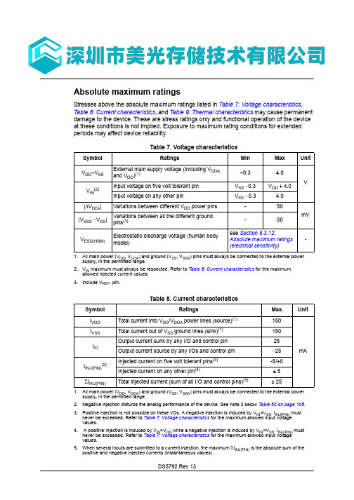
DS5792 Rev 13Absolute maximum ratingsStresses above the absolute maximum ratings listed in Table 7: Voltage characteristics , Table 8: Current characteristics , and Table 9: Thermal characteristics may cause permanent damage to the device. These are stress ratings only and functional operation of the device at these conditions is not implied. Exposure to maximum rating conditions for extended periods may affect device reliability.Table 7. Voltage characteristicsSymbol RatingsMin Max UnitV DD –V SS External main supply voltage (including V DDAand V DD)(1)1.All main power (V DD , V DDA ) and ground (V SS , V SSA ) pins must always be connected to the external powersupply, in the permitted range.–0.3 4.0V V IN (2)2.V IN maximum must always be respected. Refer to Table 8: Current characteristics for the maximumallowed injected current values.Input voltage on five volt tolerant pin V SS − 0.3V DD + 4.0 Input voltage on any other pinV SS − 0.34.0|ΔV DDx |Variations between different V DD power pins -50mV |V SSX − V SS |Variations between all the different ground pins (3)3.Include V REF- pin.-50V ESD(HBM)Electrostatic discharge voltage (human body model)see Section 5.3.12:Absolute maximum ratings (electrical sensitivity)-Table 8. Current characteristicsSymbol RatingsMax.UnitI VDD Total current into V DD /V DDA power lines (source)(1)1.All main power (V DD , V DDA ) and ground (V SS , V SSA ) pins must always be connected to the external powersupply, in the permitted range.150mA I VSS Total current out of V SS ground lines (sink)(1)150I IO Output current sunk by any I/O and control pin 25Output current source by any I/Os and control pin − 25I INJ(PIN)(2)2.Negative injection disturbs the analog performance of the device. See note 3 below Table 62 on page 108.Injected current on five volt tolerant pins (3)3.Positive injection is not possible on these I/Os. A negative injection is induced by V IN <V SS . I INJ(PIN) mustnever be exceeded. Refer to Table 7: Voltage characteristics for the maximum allowed input voltage values.-5/+0Injected current on any other pin (4)4.A positive injection is induced by V IN >V DD while a negative injection is induced by V IN <V SS . I INJ(PIN) must never be exceeded. Refer to Table 7: Voltage characteristics for the maximum allowed input voltage values.± 5ΣI INJ(PIN)Total injected current (sum of all I/O and control pins)(5)5.When several inputs are submitted to a current injection, the maximum ΣI INJ(PIN) is the absolute sum of thepositive and negative injected currents (instantaneous values).± 25Electrical characteristics STM32F103xC, STM32F103xD, STM32F103xEDS5792 Rev 135.3 Operating conditions5.3.1General operating conditionsTable 9. Thermal characteristicsSymbol RatingsValue Unit T STG Storage temperature range –65 to +150°C T JMaximum junction temperature150°CTable 10. General operating conditionsSymbol ParameterConditionsMin Max Unitf HCLK Internal AHB clock frequency -0 72MHz f PCLK1Internal APB1 clock frequency -0 36f PCLK2Internal APB2 clock frequency -0 72V DDStandard operating voltage -2 3.6V V DDA (1)1.When the ADC is used, refer to Table 59: ADC characteristics .Analog operating voltage(ADC not used)Must be the same potential as V DD (2)2.It is recommended to power V DD and V DDA from the same source. A maximum difference of 300mVbetween V DD and V DDA can be tolerated during power-up and operation.2 3.6VAnalog operating voltage (ADC used)2.43.6V BATBackup operating voltage- 1.8 3.6V P DPower dissipation at T A = 85°C for suffix 6 or T A = 105°C for suffix 7(3)3.If T A is lower, higher P D values are allowed as long as T J does not exceed T J max (see Table 6.7: Thermalcharacteristics on page 132).LQFP144-666mW LQFP100-434LQFP64-444LFBGA100-500LFBGA144-500WLCSP64-400T AAmbient temperature for 6 suffix versionMaximum power dissipation -4085°C Low-power dissipation (4)4.In low-power dissipation state, T A can be extended to this range as long as T J does not exceed T J max (seeTable 6.7: Thermal characteristics on page 132).-40105Ambient temperature for 7 suffix versionMaximum power dissipation -40105°CLow-power dissipation (4)-40125T JJunction temperature range6 suffix version -40105°C7 suffix version-40125DS5792 Rev 13STM32F103xC, STM32F103xD, STM32F103xE Electrical characteristics5.3.2 Operating conditions at power-up / power-downThe parameters given in Table 11 are derived from tests performed under the ambienttemperature condition summarized in Table 10.5.3.3 Embedded reset and power control block characteristicsThe parameters given in Table 12 are derived from tests performed under ambient temperature and V DD supply voltage conditions summarized in Table 10.Table 11. Operating conditions at power-up / power-downSymbol ParameterConditionsMin Max Unit t VDDV DD rise time rate -0∞µs/VV DD fall time rate20∞Table 12. Embedded reset and power control block characteristicsSymbolParameterConditionsMin Typ Max UnitV PVDProgrammable voltage detector level selection PLS[2:0]=000 (rising edge) 2.1 2.18 2.26V PLS[2:0]=000 (falling edge)2 2.08 2.16PLS[2:0]=001 (rising edge) 2.19 2.28 2.37PLS[2:0]=001 (falling edge) 2.09 2.18 2.27PLS[2:0]=010 (rising edge) 2.28 2.38 2.48PLS[2:0]=010 (falling edge) 2.18 2.28 2.38PLS[2:0]=011 (rising edge)2.38 2.48 2.58PLS[2:0]=011 (falling edge) 2.28 2.38 2.48PLS[2:0]=100 (rising edge)2.47 2.58 2.69PLS[2:0]=100 (falling edge) 2.37 2.48 2.59PLS[2:0]=101 (rising edge) 2.57 2.68 2.79PLS[2:0]=101 (falling edge) 2.47 2.58 2.69PLS[2:0]=110 (rising edge) 2.66 2.78 2.9PLS[2:0]=110 (falling edge) 2.56 2.68 2.8PLS[2:0]=111 (rising edge) 2.76 2.883PLS[2:0]=111 (falling edge)2.66 2.78 2.9V PVDhyst (2)PVD hysteresis--100-mV V POR/PDR Power on/power down reset threshold Falling edge 1.8(1)1.The product behavior is guaranteed by design down to the minimum V POR/PDR value.1.88 1.96V Rising edge 1.84 1.922.0V PDRhyst (2)PDR hysteresis--40-mV T RSTTEMPO (2)2.Guaranteed by design.Reset temporization-12.54.5msElectrical characteristics STM32F103xC, STM32F103xD, STM32F103xEDS5792 Rev 13DS5792 Rev 13STM32F103xC, STM32F103xD, STM32F103xE Electrical characteristicsTable 14. Maximum current consumption in Run mode, code with data processingrunning from FlashSymbolParameterConditionsf HCLK Max (1)1.Guaranteed by characterization results.UnitT A = 85°CT A = 105°CI DDSupply current in Run modeExternal clock (2), all peripherals enabled 2.External clock is 8 MHz and PLL is on when f HCLK > 8 MHz.72 MHz 6970mA48 MHz5050.536 MHz 3939.524 MHz272816 MHz2020.58 MHz 1111.5External clock (2), all peripherals disabled 72 MHz 3737.548 MHz2828.536 MHz 2222.524 MHz16.51716 MHz 12.5138 MHz88Table 15. Maximum current consumption in Run mode, code with data processingrunning from RAMSymbolParameterConditionsf HCLK Max (1)1.Guaranteed by characterization results at V DD max, f HCLK max.UnitT A = 85°CT A = 105°CI DDSupply current in Run modeExternal clock (2), all peripherals enabled 2.External clock is 8 MHz and PLL is on when f HCLK > 8 MHz.72 MHz 6667mA48 MHz43.545.536 MHz 333524 MHz2324.516 MHz16188 MHz 910.5External clock (2), all peripherals disabled 72 MHz 3333.548 MHz2323.536 MHz 1818.524 MHz1313.516 MHz 1010.58 MHz66.5。
- 1、下载文档前请自行甄别文档内容的完整性,平台不提供额外的编辑、内容补充、找答案等附加服务。
- 2、"仅部分预览"的文档,不可在线预览部分如存在完整性等问题,可反馈申请退款(可完整预览的文档不适用该条件!)。
- 3、如文档侵犯您的权益,请联系客服反馈,我们会尽快为您处理(人工客服工作时间:9:00-18:30)。
Features•ARM® 32-bit Cortex®-M3 CPU Core –72 MHz maximum frequency,1.25 DMIPS/MHz (Dhrystone2.1)performance at 0 wait state memoryaccess–Single-cycle multiplication and hardware division•Memories–64 or 128 Kbytes of Flash memory–20 Kbytes of SRAM•Clock, reset and supply management – 2.0 to 3.6 V application supply and I/Os–POR, PDR, and programmable voltage detector (PVD)–4-to-16 MHz crystal oscillator–Internal 8 MHz factory-trimmed RC–Internal 40 kHz RC–PLL for CPU clock–32 kHz oscillator for RTC with calibration •Low-power–Sleep, Stop and Standby modes–V BAT supply for RTC and backup registers • 2 x 12-bit, 1 µs A/D converters (up to 16channels)–Conversion range: 0 to 3.6 V–Dual-sample and hold capability–Temperature sensor•DMA–7-channel DMA controller–Peripherals supported: timers, ADC, SPIs, I2Cs and USARTs•Up to 80 fast I/O ports–26/37/51/80 I/Os, all mappable on 16 external interrupt vectors and almost all5 V-tolerant •Debug mode–Serial wire debug (SWD) & JTAGinterfaces•7 timers–Three 16-bit timers, each with up to 4 IC/OC/PWM or pulse counter andquadrature (incremental) encoder input –16-bit, motor control PWM timer with dead-time generation and emergency stop – 2 watchdog timers (Independent andWindow)–SysTick timer 24-bit downcounter•Up to 9 communication interfaces–Up to 2 x I2C interfaces (SMBus/PMBus)–Up to 3 USARTs (ISO 7816 interface, LIN, IrDA capability, modem control)–Up to 2 SPIs (18 Mbit/s)–CAN interface (2.0B Active)–USB 2.0 full-speed interface•CRC calculation unit, 96-bit unique ID •Packages are ECOPACK®Table 1. Device summaryReference Part numberSTM32F103x8STM32F103C8, STM32F103R8STM32F103V8, STM32F103T8STM32F103xBSTM32F103RB STM32F103VB,STM32F103CB, STM32F103TB找Memory、FPGA、二三极管、连接器、模块、光耦、电容电阻、单片机、处理器、晶振、传感器、滤波器,上深圳市美光存储技术有限公司August 20152.2 Full compatibility throughout the familyThe STM32F103xx is a complete family whose members are fully pin-to-pin, software andfeature compatible. In the reference manual, the STM32F103x4 and STM32F103x6 areidentified as low-density devices, the STM32F103x8 and STM32F103xB are referred to asmedium-density devices, and the STM32F103xC, STM32F103xD and STM32F103xE arereferred to as high-density devices.Low- and high-density devices are an extension of the STM32F103x8/B devices, they arespecified in the STM32F103x4/6 and STM32F103xC/D/E datasheets, respectively. Low-density devices feature lower Flash memory and RAM capacities, less timers andperipherals. High-density devices have higher Flash memory and RAM capacities, andadditional peripherals like SDIO, FSMC, I2S and DAC, while remaining fully compatible withthe other members of the STM32F103xx family.The STM32F103x4, STM32F103x6, STM32F103xC, STM32F103xD and STM32F103xEare a drop-in replacement for STM32F103x8/B medium-density devices, allowing the userto try different memory densities and providing a greater degree of freedom during thedevelopment cycle.Moreover, the STM32F103xx performance line family is fully compatible with all existingSTM32F101xx access line and STM32F102xx USB access line devices.2.3.13 DMAThe flexible 7-channel general-purpose DMA is able to manage memory-to-memory,peripheral-to-memory and memory-to-peripheral transfers. The DMA controller supportscircular buffer management avoiding the generation of interrupts when the controllerreaches the end of the buffer.Each channel is connected to dedicated hardware DMA requests, with support for softwaretrigger on each channel. Configuration is made by software and transfer sizes betweensource and destination are independent.The DMA can be used with the main peripherals: SPI, I2C, USART, general-purpose andadvanced-control timers TIMx and ADC.Description STM32F103x8, STM32F103xBAdvanced-control timer (TIM1)The advanced-control timer (TIM1) can be seen as a three-phase PWM multiplexed on 6channels. It has complementary PWM outputs with programmable inserted dead-times. Itcan also be seen as a complete general-purpose timer. The 4 independent channels can beused for•Input capture•Output compare•PWM generation (edge- or center-aligned modes)•One-pulse mode outputIf configured as a general-purpose 16-bit timer, it has the same features as the TIMx timer. Ifconfigured as the 16-bit PWM generator, it has full modulation capability (0-100%).In debug mode, the advanced-control timer counter can be frozen and the PWM outputsdisabled to turn off any power switch driven by these outputs.Many features are shared with those of the general-purpose TIM timers which have thesame architecture. The advanced-control timer can therefore work together with the TIMtimers via the Timer Link feature for synchronization or event chaining.General-purpose timers (TIMx)There are up to three synchronizable general-purpose timers embedded in theSTM32F103xx performance line devices. These timers are based on a 16-bit auto-reloadup/down counter, a 16-bit prescaler and feature 4 independent channels each for inputcapture/output compare, PWM or one-pulse mode output. This gives up to 12 inputcaptures/output compares/PWMs on the largest packages.The general-purpose timers can work together with the advanced-control timer via the TimerLink feature for synchronization or event chaining. Their counter can be frozen in debugmode. Any of the general-purpose timers can be used to generate PWM outputs. They allhave independent DMA request generation.These timers are capable of handling quadrature (incremental) encoder signals and thedigital outputs from 1 to 3 hall-effect sensors.Independent watchdogThe independent watchdog is based on a 12-bit downcounter and 8-bit prescaler. It isclocked from an independent 40 kHz internal RC and as it operates independently of themain clock, it can operate in Stop and Standby modes. It can be used either as a watchdogto reset the device when a problem occurs, or as a free-running timer for application timeoutmanagement. It is hardware- or software-configurable through the option bytes. The countercan be frozen in debug mode.Window watchdogThe window watchdog is based on a 7-bit downcounter that can be set as free-running. Itcan be used as a watchdog to reset the device when a problem occurs. It is clocked fromthe main clock. It has an early warning interrupt capability and the counter can be frozen indebug mode.。