5082-F157-00000中文资料
5082-5723-FJ000中文资料

14.2 mm (0.56 inch)Seven Segment Displays Technical DataFeatures• Industry Standard Size • Industry Standard Pinout 15.24 mm (0.6 in.) DIP Leads on 2.54 mm (0.1 in.) Centers • Choice of ColorsAlGaAs Red, High Efficiency Red, Yellow, Green, Orange • Excellent Appearance Evenly Lighted Segments Mitered Corners on Segments Gray Package Gives Optimum Contrast±50° Viewing Angle • Design FlexibilityCommon Anode or Common CathodeSingle and Dual Digits Right Hand Decimal Point ±1. Overflow Character• Categorized for Luminous IntensityYellow and Green Categorized for ColorUse of Like Categories Yields a Uniform Display • High Light Output • High Peak Current• Excellent for Long Digit String Multiplexing • Intensity and Color Selection OptionSee Intensity and ColorSelected Displays Data Sheet • Sunlight Viewable AlGaAsDescriptionThe 14.2 mm (0.56 inch) LED seven segment displays aredesigned for viewing distances upto 7 metres (23 feet). Thesedevices use an industry standard size package and pinout. Both the numeric and ±1 overflow devices feature a right hand decimalpoint. All devices are available as either common anode or common cathode.Orange AlGaAs Red HERYellowGreen Package HDSP-HDSP-[1]HDSP-[1]HDSP-HDSP- DescriptionDrawingH401H151550157015601Common Anode Right Hand Decimal A H403H153550357035603Common Cathode Right Hand Decimal B H157550757075607Common Anode ±1. Overflow C H158550857085608Common Cathode ±1. OverflowD K401552157215621Two Digit Common Anode Right Hand DecimalE K403552357235623Two Digit Common Cathode Right Hand DecimalFDevicesNote:1. These displays are recommended for high ambient light operation. Please refer to the HDSP-H10X/K12X AlGaAs and HDSP-555X HER data sheet for low current operation.HDSP-K40x Series HDSP-550x Series HDSP-552x Series HDSP-560x Series HDSP-562x Series HDSP-570x Series HDSP-572x Series HDSP-H15x Series HDSP-H40x SeriesThese displays are ideal for most applications. Pin for pin equivalent displays are alsoavailable in a low current design.The low current displays are idealfor portable applications. For additional information see the Low Current Seven Segment Displays data sheet.Part Numbering SystemNotes:1. For codes not listed in the figure above, please refer to the respective datasheet or contact your nearest Agilent representative for details.2. Bin options refer to shippable bins for a part number. Color and Intensity Bins are typically restricted to 1bin per tube (exceptions may apply). Please refer to respective datasheet for specific bin limit information.5082 -X X X X-X X X X X HDSP-X X X X-X X X X XMechanical Options [1]00: No Mechanical Option Color Bin Options [1,2]0: No Color Bin LimitationMaximum Intensity Bin [1,2]0: No Maximum Intensity Bin Limitation Minimum Intensity Bin [1,2]0: No Minimum Intensity Bin Limitation Device Configuration/Color [1]1: Common Anode 3: Common CathodeDevice Specific Configuration [1]Refer to Respective DatasheetPackage [1]H: 14.2 mm (0.56 inch) Single Digit Seven Segment DisplayFUNCTIONPIN AB CDEF1CATHODE e ANODE e CATHODE c ANODE cE CATHODE NO. 1 E ANODE NO. 12CATHODE d ANODE d ANODE c, d CATHODE c, d D CATHODE NO. 1 D ANODE NO. 13ANODE [3]CATHODE [4]CATHODE b ANODE bC CATHODE NO. 1 C ANODE NO. 14CATHODE c ANODE c ANODE a, b, DP CATHODE a, b, DP DP CATHODE NO. 1DP ANODE NO. 15CATHODE DP ANODE DP CATHOPDE DP ANODE DE E CATHODE NO. 1 E ANODE NO. 26CATHODE b ANODE b CATHODE a ANODE aD CATHODE NO. 2 D ANODE NO. 27CATHODE a ANODE a ANODE a, b, DP CATHODE a, b, DP G CATHODE NO. 2G ANODE NO. 28ANODE [3]CATHODE [4]ANODE c, d CATHODE c, d C CATHODE NO. 2 C ANODE NO. 29CATHODE f ANODE f CATHODE d ANODE d DP CATHODE NO. 2DP ANODE NO. 210CATHODE g ANODE g NO PINNO PINB CATHODE NO. 2 B ANODE NO. 211 A CATHODE NO. 2 A ANODE NO. 212 F CATHODE NO. 2 F ANODE NO. 213DIGIT NO. 2 ANODE DIGIT NO. 2 CATHODE 14DIGIT NO. 1 ANODE DIGIT NO. 1 CATHODE 15 B CATHODE NO. 1 B ANODE NO. 116 A CATHODE NO. 1 A ANODE NO. 117G CATHODE NO. 1G ANODE NO. 118F CATHODE NO. 1 F ANODE NO. 1NOTES:1. ALL DIMENSIONS IN MILLIMETRES (INCHES).2. ALL UNTOLERANCED DIMENSIONS ARE FOR REFERENCE ONLY.3. REDUNDANT ANODES.4. REDUNDANT CATHODES.5. FOR HDSP-5600/-5700 SERIES PRODUCT ONLY.Package DimensionsInternal Circuit DiagramNotes:1. See Figure 2 to establish pulsed conditions.2. Derate above 46°C at 0.54 mA/°C.3. See Figure 7 to establish pulsed conditions.4. Derate above 53°C at 0.45 mA/°C.5. See Figure 8 to establish pulsed conditions.HER/Orange HDSP-5500AlGaAs Red HDSP-H40x Yellow Green HDSP-H150HDSP-K40x HDSP-5700HDSP-5600 Description SeriesSeriesSeriesSeriesUnits Average Power per Segment or DP 9610580105mW Peak Forward Current per 160[1]90[3]60[5]90[7]mA Segment or DPDC Forward Current per Segment or DP 40[2]30[4]20[6]3018]mA Operating Temperature Range -20 to +100[9]-40 to +100°C Storage Temperature Range -55 to +100°C Reverse Voltage per Segment or DP 3.0V Lead Solder Temperature for 3 Seconds 260°C(1.60 mm [0.063 in.] below seating plane)Absolute Maximum Ratings6. Derate above 81°C at 0.52 mA/°C.7. See Figure 9 to establish pulsed conditions.8. Derate above 39°C at 0.37 mA/°C.9. For operation below -20°C, contact your local Agilent components sales office or an authorized distributor.Electrical/Optical Characteristics at T A = 25°CAlGaAs RedDeviceSeriesHDSP- Parameter Symbol Min.Typ.Max.Units Test Conditions Luminous Intensity/Segment[1,2,5]I V9.116.0mcd I F = 20 mA(Digit Average)1.8I F = 20 mAForward Voltage/Segment or DP V F V2.03.0I F = 100 mAH15XPeak WavelengthλPEAK645nmDominant Wavelength[3]λd637nmReverse Voltage/Segment or DP[4]V R 3.015V I R = 100 µATemperature Coefficient of∆V F/°C-2mV/°CV F/Segment or DPThermal Resistance LED Junction-RθJ-Pin400°C/W/to-Pin SegHigh Efficiency RedDeviceSeriesHDSP- Parameter Symbol Min.Typ.Max.Units Test Conditions9002800I F = 10 mA Luminous Intensity/Segment[1,2,6]I Vµcd(Digit Average)3700I F = 60 mA Peak:1 of 6 dfForward Voltage/Segment or DP V F 2.1 2.5V I F = 20 mA 55XXPeak WavelengthλPEAK635nmDominant Wavelength[3]λd626nmReverse Voltage/Segment or DP[4]V R 3.030V I R = 100 µATemperature Coefficient of∆V F/°C-2mV/°CV F/Segment or DPThermal Resistance LED Junction-RθJ-Pin345°C/W/to-Pin SegYellowDeviceSeriesHDSP- Parameter Symbol Min.Typ.Max.Units Test Conditions6001800I F = 10 mA Luminous Intensity/Segment[1,2]I Vµcd(Digit Average)2750I F = 60 mA Peak:1 of 6 dfForward Voltage/Segment or DP V F 2.1 2.5V I F = 20 mA 57XXPeak WavelengthλPEAK583nmDominant Wavelength[3,7]λd581.5586592.5nmReverse Voltage/Segment or DP[4]V R 3.040V I R = 100 µATemperature Coefficient of∆V F/°C-2mV/°CV F/Segment or DPThermal Resistance LED Junction-RθJ-Pin345°C/W/to-Pin SegOrangeDeviceSeriesHDSP- Parameter Symbol Min.Typ.Max.Units Test Conditions Luminous Intensity/Segment I V 2.37mcd I F = 10 mA(Segment Average)[1,2]Forward Voltage/Segment or DP V F 2.1 2.5V I F = 20 mAPeak WavelengthλPEAK600nm H40x Dominant Wavelength[3]λd603nm I F = 10 mA K40x Reverse Voltage/Segment or DP[4]V R 3.030V I R = 100 µA Temperature Coefficient of∆V F/°C-2mV/°CV F/Segment or DPThermal Resistance LED Junction-RθJ-Pin345°C/W/to-Pin SegDeviceSeries HDSP-ParameterSymbol Min.Typ.Max.UnitsTest Conditions 9002500I F = 10 mALuminous Intensity/Segment [1,2]I Vµcd(Digit Average)`3100I F = 60 mA Peak:1 of 6 df Forward Voltage/Segment or DPV F 2.1 2.5V I F = 10 mA56XXPeak Wavelength λPEAK 566nm Dominant Wavelength [3,7]λd 571577nm Reverse Voltage/Segment or DP [4]V R 3.050V I R = 100 µATemperature Coefficient of ∆V F /°C -2mV/°C V F /Segment or DPThermal Resistance LED Junction-R θJ-Pin345°C/W/to-PinSegHigh Performance GreenNotes:1. Device case temperature is 25°C prior to the intensity measurement.2. The digits are categorized for luminous intensity. The intensity category is designated by a letter on the side of the package.3. The dominant wavelength, λd , is derived from the CIE chromaticity diagram and is that single wavelength which defines the color of the device.4. Typical specification for reference only. Do not exceed absolute maximum ratings.5. For low current operation, the AlGaAs HDSP-H10X series displays are recommended. They are tested at 1 mA dc/segment and are pin for pin compatible with the HDSP-H15X series.6. For low current operation, the HER HDSP-555X series displays are recommended. They are tested at 2 mA dc/segment and are pin for pin compatible with the HDSP-550X series.7. The Yellow (HDSP-5700) and Green (HDSP-5600) displays are categorized for dominant wavelength. The category is designated by a number adjacent to the luminous intensity category letter.AlGaAs RedFigure 2. Maximum Tolerable Peak Current vs. Pulse Duration – AlGaAs Red.Figure 1. Maximum Tolerable Peak Current vs.Pulse Duration – Red.Figure 3. Maximum Allowable DC Current vs.Ambient Temperature.Figure 4. Forward Current vs.Forward Voltage.HER, Yellow, Green, OrangeFigure 7. Maximum Tolerable Peak Currentvs. Pulse Duration – HER, Orange.Figure 8. Maximum Tolerable Peak Current vs. Pulse Duration – Yellow.Figure 5. Relative Luminous Intensity vs. DC Forward Current.Figure 6. Relative Efficiency (Luminous Intensity per Unit Current) vs. Peak Current.I D C M A X . – M A X I M U M D C C U R R E N T P E R S E G M E N T – m AT A – AMBIENT TEMPERATURE – °C 5030102051525354045I F – F O R W A R D C U R R E N T P E R S E G M E N T – m AV F – FORWARD VOLTAGE – VR E L A T I V E L U M I N O U S I N T E N S I T Y (N O R M A L I Z E D T O 1 A T 20 m A )I F – FORWARD CURRENT PER SEGMENT – mA204010305152535ηP E A K – N O R M A L IZ E D R E L A T I V E E F F I C I E N C YI PEAK – PEAK FORWARD CURRENTPER SEGMENT – mA40051015202530352010090807060504030T – AMBIENT TEMPERATURE – °C AI M A X – M A X I M U M D C C U R R E N T P E R S E G M E N T – m AD C 4550110120Figure 11. Forward Current vs.Forward Voltage.Figure 9. Maximum Tolerable PeakCurrent vs. Pulse Duration – Green.Figure 10. Maximum Allowable DC Current vs.Ambient Temperature.Figure 12. Relative LuminousIntensity vs. DC Forward Current.Figure 13. Relative Efficiency (Luminous Intensity per Unit Current) vs. Peak Current.Electrical/OpticalFor more information onelectrical/optical characteristics,please see Application Note 1005.Contrast EnhancementFor information on contrastenhancement please see Application Note 1015.Soldering/CleaningCleaning agents from the ketone family (acetone, methyl ethyl ketone, etc.) and from thechlorinated hydrocarbon family(methylene chloride, trichloro–ethylene, carbon tetrachloride,etc.) are not recommended for cleaning LED parts. All of these various solvents attack or dissolve the encapsulating epoxies used to form the package of plastic LED parts.For information on soldering LEDs please refer to Application Note 1027.I F – F O R W A R D C U R R E N T P E R S E G M E N T – m AV F – FORWARD VOLTAGE – VR E L A T I V E L U M I N O U S I N T E N S I T Y (N O R M A L I Z E D A T 10 m A )I F – DC FORWARD CURRENT – mAηV – R E L A T I V E E F F I C I E N C Y (N O R M A L I Z E D T O 1 A T 10 m A P E R S E G M EN T )0.6I PEAK – PEAK FORWARD CURRENTPER SEGMENT – mA902070801001.61.41.31.10.90.860504030100.71.01.21.5HDSP-H15x IV Bin Category Min.Max.K 9.2016.90L 13.8025.30M 20.7038.00N 31.1056.90O 46.6085.40Intensity Bin Limits (mcd)AlGaAs RedHDSP-550x/552x IV Bin Category Min.Max.E 0.91 1.67F 1.37 2.51G 2.05 3.76H 3.08 5.64I 4.628.64J 6.9312.70K 10.3919.04HERHDSP-570x/572xIV Bin Category Min.Max.D 0.61 1.11E 0.91 1.67F 1.37 2.51G 2.05 3.76H 3.08 5.64I 4.628.64J 6.9312.70K 10.3919.04YellowHDSP-560x/562x IV Bin Category Min.Max.E 0.91 1.67F 1.37 2.51G 2.05 3.76H 3.08 5.64I 4.618.46GreenColor CategoriesNote:All categories are established for classification of products. Products may not be available in all categories. Please contact your Agilent representatives for further clarification/information.10HDSP-H40x/K40x IV Bin Category Min.Max.B 0.77 1.17C 0.95 1.45D 1.19 1.82E 1.49 2.27F 1.85 2.89G 2.32 3.54H 2.904.43Orange元器件交易网元器件交易网/semiconductorsFor product information and a complete list ofdistributors, please go to our web site.For technical assistance call:Americas/Canada: +1 (800) 235-0312 or(408) 654-8675Europe: +49 (0) 6441 92460China: 10800 650 0017Hong Kong: (+65) 271 2451India, Australia, New Zealand: (+65) 271 2394Japan: (+81 3) 3335-8152(Domestic/Interna-tional), or 0120-61-1280(Domestic Only)Korea: (+65) 271 2194Malaysia, Singapore: (+65) 271 2054Taiwan: (+65) 271 2654Data subject to change.Copyright © 2002 Agilent Technologies, Inc.Obsoletes 5988-0383ENJanuary 17, 20025988-4273EN。
爱士顿199158产品目录号199158爱士顿摩尔系列PKZM0电动机保护电路断路器,5.5 kW,

Eaton 199158Eaton Moeller® series PKZM0 Motor-protective circuit-breaker, 5.5kW, 8 - 12 A, Push in terminalsSpécifications généralesEaton Moeller® series PKZM0 Motor-protective circuit-breaker199158401508197242575 mm109 mm45 mm0.348 kgIEC/EN 60947VDE 0660ULCSAIEC/EN 60947-4-1UL 60947-4-1CSA-C22.2 No. 60947-4-1-14 CEUL File No.: E36332UL Category Control No.: NLRV CSA File No.: 165628CSA Class No.: 3211-05PKZM0-12-PIProduct Name Catalog NumberEANProduct Length/Depth Product Height Product Width Product Weight Certifications Model CodeTurn buttonPhase-failure sensitivity (according to IEC/EN 60947-4-1, VDE 0660 Part 102)Motor protectionPhase failure sensitiveThree-pole 100,000 operations100,000 OperationsDIN rail (top hat rail) mounting optionalCan be snapped on to IEC/EN 60715 top-hat rail with 7.5 or15 mm height.40 Operations/hIII3Motor protective circuit breakerFinger and back-of-hand proof, Protection against direct contact when actuated from front (EN 50274)6000 V AC25 g, Mechanical, according to IEC/EN 60068-2-27, Half-sinusoidal shock 10 msAlso motors with efficiency class IE3Branch circuit: Manual type E if used with terminal, or suitable for group installations, (UL/CSA)-5 - 40 °C to IEC/EN 60947, VDE 0660-25 - 55 °C, Operating range≤ 0.25 %/K, residual error for T > 40°Actuator type Features Functions Number of poles Lifespan, electricalLifespan, mechanicalMounting MethodMounting positionOperating frequencyOvervoltage categoryPollution degreeProduct categoryProtectionRated impulse withstand voltage (Uimp) Shock resistanceSuitable forTemperature compensationAltitude Terminal capacity (flexible)Max. 2000 m-25 °C55 °C25 °C40 °C40 °C80 °CDamp heat, constant, to IEC 60068-2-78 Damp heat, cyclic, to IEC 60068-2-301 x (1 - 6) mm²18 - 812 mm50 Hz60 Hz12 A3 kW5.5 kW690 V690 V12 A18 kA, 600 V High Fault, Fuse, SCCR (UL/CSA)600 A, 600 V High Fault, max. Fuse, SCCR (UL/CSA) 18 kA, 600 V High Fault, CB, SCCR (UL/CSA)600 A, 600 V High Fault, max. CB, SCCR (UL/CSA)18 kA, 240 V, SCCR (UL/CSA)18 kA, 480 Y/277 V, SCCR (UL/CSA)18 kA, 600 Y/347 V, SCCR (UL/CSA)65 kA, 240 V, SCCR (UL/CSA)65 kA, 480 Y/277 V, SCCR (UL/CSA)0.5 HP 3 HP2 HP3 HP 7.5 HPAmbient operating temperature - minAmbient operating temperature - maxAmbient operating temperature (enclosed) - min Ambient operating temperature (enclosed) - max Ambient storage temperature - minAmbient storage temperature - maxClimatic proofing Terminal capacity (solid/stranded AWG)Stripping length (main cable)Rated frequency - minRated frequency - maxRated operational current (Ie)Rated operational power at AC-3, 220/230 V, 50 Hz Rated operational power at AC-3, 380/400 V, 50 Hz Rated operational voltage (Ue) - minRated operational voltage (Ue) - maxRated uninterrupted current (Iu)Short-circuit current rating (group protection) Short-circuit current rating (type E)Short-circuit release Assigned motor power at 115/120 V, 60 Hz, 1-phase Assigned motor power at 200/208 V, 60 Hz, 3-phase Assigned motor power at 230/240 V, 60 Hz, 1-phase Assigned motor power at 230/240 V, 60 Hz, 3-phase Assigned motor power at 460/480 V, 60 Hz, 3-phaseBasic device fixed 15.5 x Iu, Trip Blocks186 A, Irm, Setting range max.± 20% tolerance, Trip blocks10 HPPush in terminals0 0 012 A12 AOverload trigger: tripping class 10 A6.64 W0 W0 W0 WMeets the product standard's requirements. Meets the product standard's requirements. Meets the product standard's requirements. Meets the product standard's requirements. Meets the product standard's requirements.DA-DC-00004919.pdfDA-DC-00004889.pdfETN.PKZM0-12-PI.edzIL122024ZUpkzm0_pi.stpmotorschutzschalter_bis_32a_pi.dwg121X002121X042eaton-manual-motor-starters-pkzm-pkzm0-dimensions.eps eaton-manual-motor-starters-pkz-dimensions-002.eps eaton-manual-motor-starters-pkz-dimensions.eps Assigned motor power at 575/600 V, 60 Hz, 3-phase ConnectionNumber of auxiliary contacts (change-over contacts) Number of auxiliary contacts (normally closed contacts) Number of auxiliary contacts (normally open contacts)Overload release current setting - min Overload release current setting - max Tripping characteristicEquipment heat dissipation, current-dependent PvidHeat dissipation capacity PdissHeat dissipation per pole, current-dependent PvidStatic heat dissipation, non-current-dependent Pvs10.2.2 Corrosion resistance10.2.3.1 Verification of thermal stability of enclosures10.2.3.2 Verification of resistance of insulating materials to normal heat10.2.3.3 Resist. of insul. mat. to abnormal heat/fire by internal elect. effects10.2.4 Resistance to ultra-violet (UV) radiation Declarations of conformity eCAD model Instructions d'installation mCAD modelSchémas10.2.5 LiftingDoes not apply, since the entire switchgear needs to be evaluated.10.2.6 Mechanical impactDoes not apply, since the entire switchgear needs to be evaluated.10.2.7 InscriptionsMeets the product standard's requirements.10.3 Degree of protection of assembliesDoes not apply, since the entire switchgear needs to be evaluated.10.4 Clearances and creepage distancesMeets the product standard's requirements.10.5 Protection against electric shockDoes not apply, since the entire switchgear needs to be evaluated.10.6 Incorporation of switching devices and components Does not apply, since the entire switchgear needs to be evaluated.10.7 Internal electrical circuits and connectionsIs the panel builder's responsibility.10.8 Connections for external conductorsIs the panel builder's responsibility.10.9.2 Power-frequency electric strengthIs the panel builder's responsibility.10.9.3 Impulse withstand voltageIs the panel builder's responsibility.10.9.4 Testing of enclosures made of insulating materialIs the panel builder's responsibility.10.10 Temperature riseThe panel builder is responsible for the temperature rise calculation. Eaton will provide heat dissipation data for the devices.10.11 Short-circuit ratingIs the panel builder's responsibility. The specifications for the switchgear must be observed.10.12 Electromagnetic compatibilityIs the panel builder's responsibility. The specifications for the switchgear must be observed.Eaton Corporation plc Eaton House30 Pembroke Road Dublin 4, Ireland © 2023 Eaton. Tous droits réservés. Eaton is a registered trademark.All other trademarks areproperty of their respectiveowners./socialmediaThe device meets the requirements, provided the information in the instruction leaflet (IL) is observed.10.13 Mechanical function。
5082-H157-OL000中文资料

14.2 mm (0.56 inch)Seven Segment Displays Technical DataFeatures• Industry Standard Size • Industry Standard Pinout 15.24 mm (0.6 in.) DIP Leads on 2.54 mm (0.1 in.) Centers • Choice of ColorsAlGaAs Red, High Efficiency Red, Yellow, Green, Orange • Excellent Appearance Evenly Lighted Segments Mitered Corners on Segments Gray Package Gives Optimum Contrast±50° Viewing Angle • Design FlexibilityCommon Anode or Common CathodeSingle and Dual Digits Right Hand Decimal Point ±1. Overflow Character• Categorized for Luminous IntensityYellow and Green Categorized for ColorUse of Like Categories Yields a Uniform Display • High Light Output • High Peak Current• Excellent for Long Digit String Multiplexing • Intensity and Color Selection OptionSee Intensity and ColorSelected Displays Data Sheet • Sunlight Viewable AlGaAsDescriptionThe 14.2 mm (0.56 inch) LED seven segment displays aredesigned for viewing distances upto 7 metres (23 feet). Thesedevices use an industry standard size package and pinout. Both the numeric and ±1 overflow devices feature a right hand decimalpoint. All devices are available as either common anode or common cathode.Orange AlGaAs Red HERYellowGreen Package HDSP-HDSP-[1]HDSP-[1]HDSP-HDSP- DescriptionDrawingH401H151550157015601Common Anode Right Hand Decimal A H403H153550357035603Common Cathode Right Hand Decimal B H157550757075607Common Anode ±1. Overflow C H158550857085608Common Cathode ±1. OverflowD K401552157215621Two Digit Common Anode Right Hand DecimalE K403552357235623Two Digit Common Cathode Right Hand DecimalFDevicesNote:1. These displays are recommended for high ambient light operation. Please refer to the HDSP-H10X/K12X AlGaAs and HDSP-555X HER data sheet for low current operation.HDSP-K40x Series HDSP-550x Series HDSP-552x Series HDSP-560x Series HDSP-562x Series HDSP-570x Series HDSP-572x Series HDSP-H15x Series HDSP-H40x SeriesThese displays are ideal for most applications. Pin for pin equivalent displays are alsoavailable in a low current design.The low current displays are idealfor portable applications. For additional information see the Low Current Seven Segment Displays data sheet.Part Numbering SystemNotes:1. For codes not listed in the figure above, please refer to the respective datasheet or contact your nearest Agilent representative for details.2. Bin options refer to shippable bins for a part number. Color and Intensity Bins are typically restricted to 1bin per tube (exceptions may apply). Please refer to respective datasheet for specific bin limit information.5082 -X X X X-X X X X X HDSP-X X X X-X X X X XMechanical Options [1]00: No Mechanical Option Color Bin Options [1,2]0: No Color Bin LimitationMaximum Intensity Bin [1,2]0: No Maximum Intensity Bin Limitation Minimum Intensity Bin [1,2]0: No Minimum Intensity Bin Limitation Device Configuration/Color [1]1: Common Anode 3: Common CathodeDevice Specific Configuration [1]Refer to Respective DatasheetPackage [1]H: 14.2 mm (0.56 inch) Single Digit Seven Segment DisplayFUNCTIONPIN AB CDEF1CATHODE e ANODE e CATHODE c ANODE cE CATHODE NO. 1 E ANODE NO. 12CATHODE d ANODE d ANODE c, d CATHODE c, d D CATHODE NO. 1 D ANODE NO. 13ANODE [3]CATHODE [4]CATHODE b ANODE bC CATHODE NO. 1 C ANODE NO. 14CATHODE c ANODE c ANODE a, b, DP CATHODE a, b, DP DP CATHODE NO. 1DP ANODE NO. 15CATHODE DP ANODE DP CATHOPDE DP ANODE DE E CATHODE NO. 1 E ANODE NO. 26CATHODE b ANODE b CATHODE a ANODE aD CATHODE NO. 2 D ANODE NO. 27CATHODE a ANODE a ANODE a, b, DP CATHODE a, b, DP G CATHODE NO. 2G ANODE NO. 28ANODE [3]CATHODE [4]ANODE c, d CATHODE c, d C CATHODE NO. 2 C ANODE NO. 29CATHODE f ANODE f CATHODE d ANODE d DP CATHODE NO. 2DP ANODE NO. 210CATHODE g ANODE g NO PINNO PINB CATHODE NO. 2 B ANODE NO. 211 A CATHODE NO. 2 A ANODE NO. 212 F CATHODE NO. 2 F ANODE NO. 213DIGIT NO. 2 ANODE DIGIT NO. 2 CATHODE 14DIGIT NO. 1 ANODE DIGIT NO. 1 CATHODE 15 B CATHODE NO. 1 B ANODE NO. 116 A CATHODE NO. 1 A ANODE NO. 117G CATHODE NO. 1G ANODE NO. 118F CATHODE NO. 1 F ANODE NO. 1NOTES:1. ALL DIMENSIONS IN MILLIMETRES (INCHES).2. ALL UNTOLERANCED DIMENSIONS ARE FOR REFERENCE ONLY.3. REDUNDANT ANODES.4. REDUNDANT CATHODES.5. FOR HDSP-5600/-5700 SERIES PRODUCT ONLY.Package DimensionsInternal Circuit DiagramNotes:1. See Figure 2 to establish pulsed conditions.2. Derate above 46°C at 0.54 mA/°C.3. See Figure 7 to establish pulsed conditions.4. Derate above 53°C at 0.45 mA/°C.5. See Figure 8 to establish pulsed conditions.HER/Orange HDSP-5500AlGaAs Red HDSP-H40x Yellow Green HDSP-H150HDSP-K40x HDSP-5700HDSP-5600 Description SeriesSeriesSeriesSeriesUnits Average Power per Segment or DP 9610580105mW Peak Forward Current per 160[1]90[3]60[5]90[7]mA Segment or DPDC Forward Current per Segment or DP 40[2]30[4]20[6]3018]mA Operating Temperature Range -20 to +100[9]-40 to +100°C Storage Temperature Range -55 to +100°C Reverse Voltage per Segment or DP 3.0V Lead Solder Temperature for 3 Seconds 260°C(1.60 mm [0.063 in.] below seating plane)Absolute Maximum Ratings6. Derate above 81°C at 0.52 mA/°C.7. See Figure 9 to establish pulsed conditions.8. Derate above 39°C at 0.37 mA/°C.9. For operation below -20°C, contact your local Agilent components sales office or an authorized distributor.Electrical/Optical Characteristics at T A = 25°CAlGaAs RedDeviceSeriesHDSP- Parameter Symbol Min.Typ.Max.Units Test Conditions Luminous Intensity/Segment[1,2,5]I V9.116.0mcd I F = 20 mA(Digit Average)1.8I F = 20 mAForward Voltage/Segment or DP V F V2.03.0I F = 100 mAH15XPeak WavelengthλPEAK645nmDominant Wavelength[3]λd637nmReverse Voltage/Segment or DP[4]V R 3.015V I R = 100 µATemperature Coefficient of∆V F/°C-2mV/°CV F/Segment or DPThermal Resistance LED Junction-RθJ-Pin400°C/W/to-Pin SegHigh Efficiency RedDeviceSeriesHDSP- Parameter Symbol Min.Typ.Max.Units Test Conditions9002800I F = 10 mA Luminous Intensity/Segment[1,2,6]I Vµcd(Digit Average)3700I F = 60 mA Peak:1 of 6 dfForward Voltage/Segment or DP V F 2.1 2.5V I F = 20 mA 55XXPeak WavelengthλPEAK635nmDominant Wavelength[3]λd626nmReverse Voltage/Segment or DP[4]V R 3.030V I R = 100 µATemperature Coefficient of∆V F/°C-2mV/°CV F/Segment or DPThermal Resistance LED Junction-RθJ-Pin345°C/W/to-Pin SegYellowDeviceSeriesHDSP- Parameter Symbol Min.Typ.Max.Units Test Conditions6001800I F = 10 mA Luminous Intensity/Segment[1,2]I Vµcd(Digit Average)2750I F = 60 mA Peak:1 of 6 dfForward Voltage/Segment or DP V F 2.1 2.5V I F = 20 mA 57XXPeak WavelengthλPEAK583nmDominant Wavelength[3,7]λd581.5586592.5nmReverse Voltage/Segment or DP[4]V R 3.040V I R = 100 µATemperature Coefficient of∆V F/°C-2mV/°CV F/Segment or DPThermal Resistance LED Junction-RθJ-Pin345°C/W/to-Pin SegOrangeDeviceSeriesHDSP- Parameter Symbol Min.Typ.Max.Units Test Conditions Luminous Intensity/Segment I V 2.37mcd I F = 10 mA(Segment Average)[1,2]Forward Voltage/Segment or DP V F 2.1 2.5V I F = 20 mAPeak WavelengthλPEAK600nm H40x Dominant Wavelength[3]λd603nm I F = 10 mA K40x Reverse Voltage/Segment or DP[4]V R 3.030V I R = 100 µA Temperature Coefficient of∆V F/°C-2mV/°CV F/Segment or DPThermal Resistance LED Junction-RθJ-Pin345°C/W/to-Pin SegDeviceSeries HDSP-ParameterSymbol Min.Typ.Max.UnitsTest Conditions 9002500I F = 10 mALuminous Intensity/Segment [1,2]I Vµcd(Digit Average)`3100I F = 60 mA Peak:1 of 6 df Forward Voltage/Segment or DPV F 2.1 2.5V I F = 10 mA56XXPeak Wavelength λPEAK 566nm Dominant Wavelength [3,7]λd 571577nm Reverse Voltage/Segment or DP [4]V R 3.050V I R = 100 µATemperature Coefficient of ∆V F /°C -2mV/°C V F /Segment or DPThermal Resistance LED Junction-R θJ-Pin345°C/W/to-PinSegHigh Performance GreenNotes:1. Device case temperature is 25°C prior to the intensity measurement.2. The digits are categorized for luminous intensity. The intensity category is designated by a letter on the side of the package.3. The dominant wavelength, λd , is derived from the CIE chromaticity diagram and is that single wavelength which defines the color of the device.4. Typical specification for reference only. Do not exceed absolute maximum ratings.5. For low current operation, the AlGaAs HDSP-H10X series displays are recommended. They are tested at 1 mA dc/segment and are pin for pin compatible with the HDSP-H15X series.6. For low current operation, the HER HDSP-555X series displays are recommended. They are tested at 2 mA dc/segment and are pin for pin compatible with the HDSP-550X series.7. The Yellow (HDSP-5700) and Green (HDSP-5600) displays are categorized for dominant wavelength. The category is designated by a number adjacent to the luminous intensity category letter.AlGaAs RedFigure 2. Maximum Tolerable Peak Current vs. Pulse Duration – AlGaAs Red.Figure 1. Maximum Tolerable Peak Current vs.Pulse Duration – Red.Figure 3. Maximum Allowable DC Current vs.Ambient Temperature.Figure 4. Forward Current vs.Forward Voltage.HER, Yellow, Green, OrangeFigure 7. Maximum Tolerable Peak Currentvs. Pulse Duration – HER, Orange.Figure 8. Maximum Tolerable Peak Current vs. Pulse Duration – Yellow.Figure 5. Relative Luminous Intensity vs. DC Forward Current.Figure 6. Relative Efficiency (Luminous Intensity per Unit Current) vs. Peak Current.I D C M A X . – M A X I M U M D C C U R R E N T P E R S E G M E N T – m AT A – AMBIENT TEMPERATURE – °C 5030102051525354045I F – F O R W A R D C U R R E N T P E R S E G M E N T – m AV F – FORWARD VOLTAGE – VR E L A T I V E L U M I N O U S I N T E N S I T Y (N O R M A L I Z E D T O 1 A T 20 m A )I F – FORWARD CURRENT PER SEGMENT – mA204010305152535ηP E A K – N O R M A L IZ E D R E L A T I V E E F F I C I E N C YI PEAK – PEAK FORWARD CURRENTPER SEGMENT – mA40051015202530352010090807060504030T – AMBIENT TEMPERATURE – °C AI M A X – M A X I M U M D C C U R R E N T P E R S E G M E N T – m AD C 4550110120Figure 11. Forward Current vs.Forward Voltage.Figure 9. Maximum Tolerable PeakCurrent vs. Pulse Duration – Green.Figure 10. Maximum Allowable DC Current vs.Ambient Temperature.Figure 12. Relative LuminousIntensity vs. DC Forward Current.Figure 13. Relative Efficiency (Luminous Intensity per Unit Current) vs. Peak Current.Electrical/OpticalFor more information onelectrical/optical characteristics,please see Application Note 1005.Contrast EnhancementFor information on contrastenhancement please see Application Note 1015.Soldering/CleaningCleaning agents from the ketone family (acetone, methyl ethyl ketone, etc.) and from thechlorinated hydrocarbon family(methylene chloride, trichloro–ethylene, carbon tetrachloride,etc.) are not recommended for cleaning LED parts. All of these various solvents attack or dissolve the encapsulating epoxies used to form the package of plastic LED parts.For information on soldering LEDs please refer to Application Note 1027.I F – F O R W A R D C U R R E N T P E R S E G M E N T – m AV F – FORWARD VOLTAGE – VR E L A T I V E L U M I N O U S I N T E N S I T Y (N O R M A L I Z E D A T 10 m A )I F – DC FORWARD CURRENT – mAηV – R E L A T I V E E F F I C I E N C Y (N O R M A L I Z E D T O 1 A T 10 m A P E R S E G M EN T )0.6I PEAK – PEAK FORWARD CURRENTPER SEGMENT – mA902070801001.61.41.31.10.90.860504030100.71.01.21.5HDSP-H15x IV Bin Category Min.Max.K 9.2016.90L 13.8025.30M 20.7038.00N 31.1056.90O 46.6085.40Intensity Bin Limits (mcd)AlGaAs RedHDSP-550x/552x IV Bin Category Min.Max.E 0.91 1.67F 1.37 2.51G 2.05 3.76H 3.08 5.64I 4.628.64J 6.9312.70K 10.3919.04HERHDSP-570x/572xIV Bin Category Min.Max.D 0.61 1.11E 0.91 1.67F 1.37 2.51G 2.05 3.76H 3.08 5.64I 4.628.64J 6.9312.70K 10.3919.04YellowHDSP-560x/562x IV Bin Category Min.Max.E 0.91 1.67F 1.37 2.51G 2.05 3.76H 3.08 5.64I 4.618.46GreenColor CategoriesNote:All categories are established for classification of products. Products may not be available in all categories. Please contact your Agilent representatives for further clarification/information.10HDSP-H40x/K40x IV Bin Category Min.Max.B 0.77 1.17C 0.95 1.45D 1.19 1.82E 1.49 2.27F 1.85 2.89G 2.32 3.54H 2.904.43Orange元器件交易网元器件交易网/semiconductorsFor product information and a complete list ofdistributors, please go to our web site.For technical assistance call:Americas/Canada: +1 (800) 235-0312 or(408) 654-8675Europe: +49 (0) 6441 92460China: 10800 650 0017Hong Kong: (+65) 271 2451India, Australia, New Zealand: (+65) 271 2394Japan: (+81 3) 3335-8152(Domestic/Interna-tional), or 0120-61-1280(Domestic Only)Korea: (+65) 271 2194Malaysia, Singapore: (+65) 271 2054Taiwan: (+65) 271 2654Data subject to change.Copyright © 2002 Agilent Technologies, Inc.Obsoletes 5988-0383ENJanuary 17, 20025988-4273EN。
5082-H107-DG000中文资料

Features• Low Power Consumption • Industry Standard Size• Industry Standard Pinout • Choice of Character Size7.6 mm (0.30 in), 10 mm (0.40 in), 10.9 mm (0.43 in), 14.2 mm (0.56 in), 20 mm (0.80 in)• Choice of ColorsAlGaAs Red, High Efficiency Red (HER), Yellow, Green• Excellent Appearance Evenly Lighted Segments±50° Viewing Angle• Design FlexibilityCommon Anode or Common CathodeSingle and Dual DigitLeft and Right Hand Decimal Points±1. Overflow Character• Categorized for Luminous IntensityYellow and Green Categorized for ColorUse of Like Categories Yields a Uniform Display• Excellent for Long Digit String Multiplexing DescriptionThese low current seven segment displays are designed for applica-tions requiring low power consumption. They are tested and selected for their excellent low current characteristics to ensure that the segments are matched at low currents. Drive currents as low as 1 mA per segment are available.Pin for pin equivalent displays are also available in a standard current or high light ambient design. The standard current displays are available in all colors and are ideal for most applica-tions. The high light ambient displays are ideal for sunlight ambients or long string lengths. For additional information see the 7.6 mm Micro Bright Seven Segment Displays, 10 mm Seven Segment Displays, 7.6 mm/10.9 mm Seven Segment Displays, 14.2 mm Seven Segment Displays, 20 mm Seven Segment Displays, or High Light Ambient Seven Segment Displays data sheets.Low Current Seven SegmentDisplays Technical Data HDSP-335x SeriesHDSP-555x SeriesHDSP-751x SeriesHDSP-A10x Series HDSP-A80x Series HDSP-A90x Series HDSP-E10x Series HDSP-F10x Series HDSP-G10x Series HDSP-H10x Series HDSP-K12x, K70x Series HDSP-N10x SeriesHDSP-N40x SeriesDevicesAlGaAs HER Yellow Green Package HDSP-HDSP-HDSP-HDSP-Description Drawing A1017511A801A9017.6 mm Common Anode Right Hand Decimal A A1037513A803A9037.6 mm Common Cathode Right Hand Decimal B A1077517A807A9077.6 mm Common Anode ±1. Overflow C A1087518A808A9087.6 mm Common Cathode ±1. Overflow D F10110 mm Common Anode Right Hand Decimal E F10310 mm Common Cathode Right Hand Decimal F F10710 mm Common Anode ±1. Overflow G F10810 mm Common Cathode ±1. Overflow H G10110 mm Two Digit Common Anode Right Hand Decimal X G10310 mm Two Digit Common Cathode Right Hand Decimal Y E100335010.9 mm Common Anode Left Hand Decimal I E101335110.9 mm Common Anode Right Hand Decimal J E103335310.9 mm Common Cathode Right Hand Decimal K E106335610.9 mm Universal ±1. Overflow[1]L H101555114.2 mm Common Anode Right Hand Decimal M H103555314.2 mm Common Cathode Right Hand Decimal N H107555714.2 mm Common Anode ±1. Overflow O H108555814.2 mm Common Cathode ±1. Overflow P K121K70114.2 mm Two Digit Common Anode Right Hand Decimal R K123K70314.2 mm Two Digit Common Cathode Right Hand Decimal S N10020 mm Common Anode Left Hand Decimal Q N101N40120 mm Common Anode Right Hand Decimal T N103N40320 mm Common Cathode Right Hand Decimal U N10520 mm Common Cathode Left Hand Decimal V N106N40620 mm Universal ±1. Overflow[1]W Note:1. Universal pinout brings the anode and cathode of each segment’s LED out to separate pins. See internal diagrams L or W.Part Numbering System5082-x xx x-x x x xxHDSP-x xx x-x x x xxMechanical Options[1]00: No mechanical optionColor Bin Options[1,2]0: No color bin limitationMaximum Intensity Bin[1,2]0: No maximum intensity bin limitationMinimum Intensity Bin[1,2]0: No minimum intensity bin limitationDevice Configuration/Color[1]G: GreenDevice Specific Configuration[1]Refer to respective datasheetPackage[1]Refer to Respective datasheetNotes:1. For codes not listed in the figure above, please refer to the respective datasheet or contact your nearest Agilent representative fordetails.2. Bin options refer to shippable bins for a part-number. Color and Intensity Bins are typically restricted to 1 bin per tube (excep-tions may apply). Please refer to respective datasheet for specific bin limit information.Package DimensionsPackage Dimensions (cont.)Package Dimensions (cont.)*The Side View of package indicates Country of Origin.Package Dimensions (cont.)Package Dimensions (cont.)Package Dimensions (cont.)Internal Circuit DiagramInternal Circuit Diagram (cont.)Absolute Maximum RatingsAlGaAs Red - HDSP-HERA10X/E10X/H10X HDSP-751X/Yellow GreenK12X/N10X/N40X335X/555X/HDSP-A80X HDSP-A90X Description F10X, G10X Series K70X Series Series Series Units Average Power per Segment or DP375264mW Peak Forward Current per 45mA Segment or DPDC Forward Current per15[1]15[2]mA Segment or DPOperating Temperature Range-20 to +100-40 to +100°C Storage Temperature Range -55 to +100°C Reverse Voltage per Segment 3.0V or DPWave Soldering Temperature for 3Seconds (1.60 mm [0.063 in.] below 250°C seating body)Notes:1. Derate above 91°C at 0.53 mA/°C.2. Derate HER/Yellow above 80°C at 0.38 mA/°C and Green above 71°C at 0.31 mA/°C.Electrical/Optical Characteristics at T A = 25°CAlGaAs RedDeviceSeriesHDSP-Parameter Symbol Min.Typ.Max.Units Test Conditions315600I F = 1 mA A10x3600I F = 5 mA330650I F = 1 mAF10x, G10x3900I F = 5 mA390650I F = 1 mA E10x Luminous Intensity/Segment[1,2]I Vµcd(Digit Average)3900I F = 5 mA400700I F = 1 mAH10x, K12x4200I F = 5 mA270590I F = 1 mAN10x, N40x3500I F = 5 mA1.6I F = 1 mAForward Voltage/Segment or DP V F 1.7V I F = 5 mA1.82.2I F = 20 mA PkAll Devices Peak WavelengthλPEAK645nmDominant Wavelength[3]λd637nmReverse Voltage/Segment or DP[4]V R 3.015V I R = 100 µATemperature Coefficient of∆V F/°C-2 mV mV/°CV F/Segment or DPA10x255F10x, G10x320E10x340Thermal Resistance LED RθJ-PIN°C/W/SegH10x, K12x Junction-to-Pin400N10x, N40x430High Efficiency RedDeviceSeriesHDSP-Parameter Symbol Min.Typ.Max.Units Test Conditions160270I F = 2 mA 751x1050I F = 5 mA200300I F = 2 mA Luminous Intensity/Segment[1,2]I V mcd(Digit Average)1200I F = 5 mA335x, 555x,K70x270370I F = 2 mA1480I F = 5 mA1.6I F = 2 mAForward Voltage/Segment or DP V F 1.7V I F = 5 mA2.1 2.5I F = 20 mA Pk All Devices Peak WavelengthλPEAK635nmDominant Wavelength[3]λd626nmReverse Voltage/Segment or DP[4]V R 3.030V I R = 100 µATemperature Coefficient of∆V F/°C-2mV/°CV F/Segment or DP751x200335x Thermal Resistance LED RθJ-PIN280°C/WJunction-to-Pin555x, K70x345YellowDeviceSeriesHDSP-Parameter Symbol Min.Typ.Max.Units Test Conditions Luminous Intensity/Segment[1,2]250420I F = 4 mA(Digit Average)I V mcd1300I F = 10 mA1.7I F = 4 mAForward Voltage/Segment or DP V F 1.8V I F = 5 mA A80x2.1 2.5I F = 20 mA PkPeak WavelengthλPEAK583nmDominant Wavelength[3,5]λd581.5585592.5nmReverse Voltage/Segment or DP[4]V R 3.030V I R = 100 µATemperature Coefficient of∆V F/°C-2mV/°CV F/Segment or DPThermal Resistance LED RθJ-PIN200°C/WJunction-to-PinGreenDeviceSeriesHDSP-Parameter Symbol Min.Typ.Max.Units Test Conditions Luminous Intensity/Segment[1,2]250475I F = 4 mA(Digit Average)I V mcd1500I F = 10 mA1.9I F = 4 mAForward Voltage/Segment or DP V F 2.0V I F = 10 mA A90x2.1 2.5I F = 20 mA PkPeak WavelengthλPEAK566nmDominant Wavelength[3,5]λd571577nmReverse Voltage/Segment or DP[4]V R 3.030V I R = 100 µATemperature Coefficient of∆V F/°C-2mV/°CV F/Segment or DPThermal Resistance LED RθJ-PIN200°C/WJunction-to-PinNotes:1. Device case temperature is 25°C prior to the intensity measurement.2. The digits are categorized for luminous intensity. The intensity category is designated by a letter on the side of the package.3. The dominant wavelength, λd, is derived from the CIE chromaticity diagram and is the single wavelength which defines the color of thedevice.4. Typical specification for reference only. Do not exceed absolute maximum ratings.5. The yellow (HDSP-A800) and Green (HDSP-A900) displays are categorized for dominant wavelength. The category is designated by anumber adjacent to the luminous intensity category letter.AlGaAs RedIntensity Bin Limits (mcd)AlGaAs RedHDSP-A10xIV Bin Category Min.Max.E0.3150.520F0.4280.759G0.621 1.16H0.945 1.71I 1.40 2.56J 2.10 3.84K 3.14 5.75L 4.708.55HDSP-E10x/F10x/G10xIV Bin Category Min.Max.D0.3910.650E0.5320.923F0.755 1.39G 1.13 2.08H 1.70 3.14HDSP-H10x/K12xIV Bin Category Min.Max.C0.4150.690D0.5650.990E0.810 1.50F 1.20 2.20G 1.80 3.30H 2.73 5.00I 4.097.50HDSP-N10xIV Bin Category Min.Max.A0.2700.400B0.3250.500C0.4150.690D0.5650.990E0.810 1.50F 1.20 2.20G 1.80 3.30H 2.73 5.00I 4.097.50Intensity Bin Limits (mcd), continued HERHDSP-751xIV Bin Category Min.Max.B0.1600.240C0.2000.300D0.2500.385E0.3150.520F0.4280.759G0.621 1.16HDSP-751xIV Bin Category Min.Max.B0.2400.366C0.3000.477D0.3910.650E0.5320.923F0.755 1.39G 1.13 2.08H 1.70 3.14HDSP-555x/K70xIV Bin Category Min.Max.A0.2700.400B0.3250.500C0.4150.690D0.5650.990E0.810 1.50F 1.20 2.20G 1.80 3.30H 2.73 5.00I 4.097.50Intensity Bin Limits (mcd), continued YellowHDSP-A80xIV Bin Category Min.Max.D0.2500.385E0.3150.520F0.4250.760G0.625 1.14H0.940 1.70I 1.40 2.56J 2.10 3.84K 3.14 5.76L 4.718.64M7.0713.00N10.6019.40O15.9029.20P23.9043.80Q35.8065.60GreenHDSP-A90xIV Bin Category Min.Max.E0.3150.520F0.4250.760G0.625 1.14H0.940 1.70I 1.40 2.56J 2.10 3.84K 3.14 5.76L 4.718.64M7.0713.00N10.6019.40O15.9029.20P23.9043.80Q35.8065.60Electrical/OpticalFor more information on electrical/optical characteristics, please see Application Note 1005.Contrast Enhancement For information on contrast enhancement, please see Application Note 1015.Soldering/Cleaning Cleaning agents from the ketone family (acetone, methyl ethyl ketone, etc.) and from the chorinated hydrocarbon family (methylene chloride, trichloro-ethylene, carbon tetrachloride, etc.) are not recommended for cleaning LED parts. All of these various solvents attack or dissolve the encapsulating epoxies used to form the package of plastic LED parts.For information on soldering LEDs, please refer to Application Note 1027.Note:All categories are established for classification of products. Productsmay not be available in all categories. Please contact your localAgilent representatives for further clarification/information.Color Categories/semiconductorsFor product information and a complete list ofdistributors, please go to our web site.For technical assistance call:Americas/Canada: +1 (800) 235-0312 or(916) 788 6763Europe: +49 (0) 6441 92460China: 10800 650 0017Hong Kong: (+65) 6271 2451India, Australia, New Zealand: (+65) 6271 2394Japan: (+81 3) 3335-8152(Domestic/International), or0120-61-1280(Domestic Only)Korea: (+65) 6271 2194Malaysia, Singapore: (+65) 6271 2054Taiwan: (+65) 6271 2654Data subject to change.Copyright © 2005 Agilent Technologies, Inc.Obsoletes 5988-8412ENJanuary 19, 20055989-0080EN。
5082-B05G-LK000中文资料
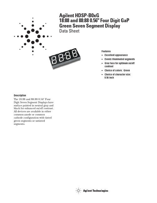
DescriptionThe 18:88 and 88:88 0.56" Four Digit Seven Segment Displays have surface painted in neutral gray and black for enhanced on/off contrast. All devices are available in either common anode or common cathode configuration with tinted green segments or untinted segments.Agilent HDSP-B0xG18:88 and 88:88 0.56" Four Digit GaP Green Seven Segment DisplayData SheetFeatures•Excellent appearance•Evenly illuminated segments•Gray face for optimum on/offcontrast•Choice of colors: Green•Choice of character size:0.56 inchFRONT SIDE2 – ∅1.70RIGHT SIDEA A A DDD C F EF E F EB CB C B C GGGDP3DP2DIGIT 2DIGIT 3DIGIT 4DIGIT 1AF EB G D NOTE:ALL DIMENSIONS ARE IN MILLIMETERS (INCHES).UNLESS OTHERWISE STATED, TOLERANCES ARE ± 0.25 mm.Pin Configuration Function Pin HDSP-B01G/B03G/B05G/B07G/B09G HDSP-B02G/B04G/B06G/B08G/B10G 1Anode E Cathode E 2Anode D Cathode D 3Anode DP Cathode DP 4Anode C Cathode C 5Anode GCathode G6Digit 4 Common Cathode Digit 4 Common Anode 7Anode BCathode B8Digit 3 Common Cathode Digit 3 Common Anode 9Digit 2 Common Cathode Digit 2 Common Anode 10Anode F Cathode F 11Anode ACathode A12Digit 1 Common CathodeDigit 1 Common AnodeFRONT SIDE2 – ∅1.70RIGHT SIDEAA A DDD B CF EF E F EB CB C B C GGGDP3DP2DIGIT 2DIGIT 3DIGIT 4DIGIT 1NOTE:ALL DIMENSIONS ARE IN MILLIMETERS (INCHES).UNLESS OTHERWISE STATED, TOLERANCES ARE ± 0.25 mm.HDSP-B01G and HDSP-B05G (Common Cathode)HDSP-B02G and HDSP-B06G (Common Anode)DIGIT 1DIGIT 2DIGIT 3DIGIT 4A 11B 7C 4D 2E 1F 10G 5DP 3DIGIT 1DIGIT 2DIGIT 3DIGIT 4A 11B 7C 4D 2E 1F 10G 5DP 3HDSP-B03G, HDSP-B07G, and HDSP-B09G (Common Cathode)HDSP-B04G, HDSP-B08G, and HDSP-B10G (Common Anode)DIGIT 1DIGIT 2DIGIT 3DIGIT 4A 11B 7C 4D 2E 1F 10G 5DP3DIGIT 1DIGIT 2DIGIT 3DIGIT 4A 11B 7C 4D 2E 1F 10G 5DP 3DevicesHDSP-DescriptionB01G88:88 0.56" Green 4 Digit, Tinted Green, Common Cathode, Display 18:88, Gray Color Surface B02G88:88 0.56" Green 4 Digit, Tinted Green, Common Anode, Display 18:88, Gray Color Surface B03G88:88 0.56" Green 4 Digit, Tinted Green, Common Cathode, Display 88:88, Gray Color Surface B04G88:88 0.56" Green 4 Digit, Tinted Green, Common Anode, Display 88:88, Gray Color Surface B05G88:88 0.56" Green 4 Digit, Untinted, Common Cathode, Display 18:88, Gray Color SurfaceB06G88:88 0.56" Green 4 Digit, Untinted, Common Anode, Display 18:88, Gray Color SurfaceB07G88:88 0.56" Green 4 Digit, Untinted, Common Cathode, Display 88:88, Gray Color SurfaceB08G88:88 0.56" Green 4 Digit, Untinted, Common Anode, Display 88:88, Gray Color SurfaceB09G88:88 0.56" Green 4 Digit, Untinted, Common Cathode, Display 88:88, Black Color SurfaceB10G88:88 0.56" Green 4 Digit, Untinted, Common Anode, Display 88:88, Black Color SurfacePart Numbering System5082 -X X X X-X X X X XHDSP-X X X X-X X X X XMechanical Options[1]00: No Mechanical OptionColor Bin Options[1,2]0: No Color Bin LimitationMaximum Intensity Bin[1,2]0: No Maximum Intensity Bin LimitationMinimum Intensity Bin[1,2]0: No Minimum Intensity Bin LimitationDevice Configuration/Color[1]G: GreenDevice Specific Configuration[1]Refer to Respective DatasheetPackage[1]Refer to Respective DatasheetNotes:1. For codes not listed in the figure above, please refer to the respective datasheet or contactyour nearest Agilent representative for details.2. Bin options refer to shippable bins for a part number. Color and Intensity Bins are typicallyrestricted to 1 bin per tube (exceptions may apply). Please refer to respective datasheet forspecific bin limit information.Electrical/Optical Characteristics at T A = 25˚C Device Series HDSP-ParameterSymbol Min.Typ.Max.Units Test Conditions Luminous Intensity/SegmentI V20003200µcd I F = 10 mA(Digit Average)32004500All DevicesForward Voltage/Segment or DP V F 1.802.20 2.60V I F = 20 mA Peak Wavelength λPEAK 568nm I F = 20 mA Dominant Wavelength λd 573nmI F = 20 mA Luminous Intensity I V-M 2:1I F = 10 mA Matching Ratio Reverse CurrentI R100µAV R = 5 VNotes:1.Typical specification for reference only. Do not exceed absolute maximum ratings.2.The dominant wavelength, λd , is derived from the CIE chromaticity diagram and is that single wavelength which defines the color of the device.Absolute Maximum RatingsDescriptionGreen Units Average Power per Segment or DP65mW Peak Forward Current per Segment or DP 100mA DC Forward Current per Segment or DP 25mA Operating Temperature Range–40 to +105˚C Storage Temperature Range–40 to +105˚C Reverse Voltage per Segment or DP5V Wavesoldering Temperature for 3 seconds 2 mm below body250˚CNote:1.Derate above 40˚C at 0.33 mA/˚C for green.B01G, B02G, B03G, B04G B05G, B06G, B07G, B08G,B09G, B10G Intensity Bin Limits (µcd at 10 mA)Device Series HDSP-B01G, B02G, B03G, B04G B05G, B06G, B07G, B08G, B09G, B10GBin Name Min.[1]Max.[1]Min.[1]Max.[1]K 20003200NA NA L 3200505032005050MNA NA50508000Note:1.Tolerance for each bin limit is ±10%.Color Categories (Tolerance ± 1 nm)Rank Symbol Hue Range Unit 22573.5–576.5nm 33570.5–573.5nmContrast EnhancementFor information on contrast enhancement, please see Application Note 1015.Soldering/CleaningCleaning agents from the ketone family (acetone, methyl ethyl ketone, etc.) and from thechlorinated hydrocarbon family (methylene chloride,trichloroethylene, carbon tetrachloride, etc.) are notrecommended for cleaning LED parts. All these various solvents attack or dissolve theencapsulating epoxies used to form the package of plastic LED parts.Figure 1. Maximum allowable DC current vs.ambient temperature.Figure 2. Forward current vs. forward voltage.Figure 3. Relative luminous intensity vs. DC forward current.Figure 4. Relative efficiency (luminous intensity per unit current) vs. peak current.I D C – M A X I M U M D C C U R R E N T P E R S E G M E N T – m AT A – AMBIENT TEMPERATURE – °CI F – F O R W A R D C U R R E N T P E R S E G M E NT – m AV F – FORWARD VOLTAGE – VR E L A T I V E L U M I N O U S I N T E N S I T Y (N O R M A L I Z E D T O 1 A T 10 mA F O R G R E E N )I F – DC FORWARD CURRENT – mA8642R E L A T I V E E F F I C I E N C Y (N O R M A L I Z E D T O 1 A T 10 m A )1.4005101520253035404550PEAK FORWARD CURRENTPER SEGMENT – mA/semiconductorsFor product information and a complete list of distributors, please go to our web site.For technical assistance call:Americas/Canada: +1 (800) 235-0312 or (916) 788-6763Europe: +49 (0) 6441 92460China: 10800 650 0017Hong Kong: (+65) 6756 2394India, Australia, New Zealand: (+65) 6755 1939Japan: (+81 3) 3335-8152(Domestic/Interna-tional), or 0120-61-1280(Domestic Only)Korea: (+65) 6755 1989Singapore, Malaysia, Vietnam, Thailand,Philippines, Indonesia: (+65) 6755 2044Taiwan: (+65) 6755 1843Data subject to change.Copyright © 2004 Agilent Technologies, Inc.Obsoletes 5988-5381EN June 30, 20045988-7859EN。
霍尼韦尔报警系统设备参数(2015版)
报警系统设备参数报警系统设备参数目录目录1.控制主机 (5)1.14110DL控制主机 (5)1.2VISTA-10P控制主机 (6)1.3VISTA-20P控制主机 (7)1.4VISTA-120/250总线制大型控制主机 (9)1.5Vista-128BPT/ Vista-250BPT (11)1.6COMPACT-4 4防区控制主机【GPRS主机】 (12)1.7236 PLUSII控制主机 (13)1.8238C PLUSII控制主机 (14)1.9238C Super 控制主机 (15)1.102316PLUSII控制主机 (18)1.112316super 控制主机 (19)1.12L YNX家居无线控制主机 (21)2.报警模块及附件 (24)2.1报警键盘 (24)2.1.16148CH固定字符键盘 (24)2.1.26160可编程英文液晶键盘 (24)2.1.3236PLUS LED控制键盘 (25)2.1.4238CPLUS LED控制键盘 (25)2.1.52316PLUS LED控制键盘 (26)2.1.62300Alpha Plus II 控制键盘 (26)2.2VISTA系列附件 (27)2.2.14229八防区扩展模块 (27)2.2.24219八防区扩展模块 (27)2.2.34293SN单防区扩展模块 (28)2.2.44193SN双防区扩展模块 (28)2.2.54193SNP双防区扩展模块 (29)2.2.64208SN八防区扩展模块 (29)2.2.74101SN总线继电器模块 (30)2.2.84204 四路继电器联动模块 (30)2.2.94232AP 32路继电器模块 (30)2.2.104286语音模块 (32)2.2.114100SM串行接口模块 (32)2.2.12IP-2000网络接口展模块 (33)2.2.13IPM-VISTA网络接口模块 (33)2.2.14IPM-VISTA super II网络接口模块 (34)2.2.154297总线延伸模块 (35)2.2.16VSI总线隔离器 (36)2.2.17VISTA-KEY 门禁控制器模块 (36)2.2.185881 ENH 防区无线接收机 (37)2.2.19IPM-2300网络接口模块 (38)2.2.20IPM-23 SUPER II网络接口模块 (38)2.2.21MCM-23(GPRS)无线网络模块 (39)2.2.22MCM-23 Super II (GPRS)无线网络模块 (40)3.探测器&传感器 (42)3.1双鉴探测器 (42)3.1.1DT-7225T 双鉴探测器 (42)3.1.2DT-7235T双鉴探测器 (43)3.1.3DT-7435T防宠物双鉴探测器 (43)3.1.4DT-7450双鉴探测器 (44)3.1.5DT-6360STC智能型吸顶式双鉴探测器 (45)3.1.6DT-900/DT-906工、商业级双鉴探测器 (46)3.1.7DT8035双鉴探测器 (47)3.1.8DT8050双鉴探测器 (48)3.2被动红外探测器 (49)3.1.1997吸顶式被动红外探测器 (49)3.1.2IS215T被动红外探测器 (50)3.1.3IS2260T智能型防宠物被动红外探测器 (50)3.1.4IS216T-CUR幕帘被动红外探测器 (51)3.1.5SP-30QU方向识别幕帘探测器 (52)3.1.6IS-208被动红外探测器 (52)3.3玻璃破碎探测器 (54)3.1.7FG-1615T/1625T/1525RT玻璃破碎探测器 (54)3.1.8FG701玻璃破碎仿真器 (55)3.4震动红外探测器 (56)3.1.911WH震动探测器 (56)3.1.10SD3震动探测器 (56)3.1.11MA-100T震动探测器 (56)3.1.12SC100/SC105震动探测器 (57)3.1.13S100 振动探测器 (57)3.1.14SC105震动探测器 (58)3.5水/温度探测器 (59)3.1.15470-12水探测器 (59)3.1.16TS300双探头温度探测器 (59)3.6门磁开关 (60)3.1.17MPS70WGW /B暗装门磁 (60)3.1.18MPS80WGW /B表面安装门磁 (60)3.1.19MPS50表面安装门磁 (60)3.1.20MPS51表面安装门磁 (60)3.7紧急开关/紧急按钮 (61)3.1.21264钱夹开关 (61)3.1.22266脚挑紧急开关 (61)3.1.23269R/270R紧急开关 (61)3.1.25PB110紧急按钮 (62)3.8HIBS户外被动红外探测器 (63)3.1.26HIBS1双光束主动红外对射 (63)3.1.27HIBS2四光束主动红外对射 (64)3.9315MHZ无线传感器 (65)3.1.285890AP无线红外探测器 (65)3.1.295816AP小型门窗发射器 (65)3.1.305802AP便携式无线按钮 (65)3.1.315804C 四键无线按钮 (66)3.10警号与闪灯 (66)3.1.32SP20S警号 (66)3.1.33710RD闪灯 (67)3.11离子式烟雾探测器 (67)3.1.34JTY-GD-2412 和JTY-GD-2424 (67)4.接警中心设备 (69)3.1.35MX-8000-3数字接收机 (69)3.1.36Doppio(Linux)网络接收机 (70)3.1.37IP-Alarm-II 报警管理软件 (72)3.1.38VISTA Alarm Viewer总线报警主机监控软件 (73)1. 控制主机1.1 4110DL控制主机防区特性:6个基本防区,均带有末端电阻监控。
5082-F513-HK300中文资料

DevicesAlGaAs Orange Red HER Green Package HDSP-HDSP-HDSP-HDSP- DescriptionDrawingA411A111A211A5117.6 mm Common Anode Right Hand Decimal A A413A113A213A5137.6 mm Common Cathode Right Hand Decimal B F411F111F211F51110 mm Common Anode Right Hand Decimal C F413F113F213F51310 mm Common Cathode Right Hand Decimal D G411G111G211G51110 mm Two Digit Common Anode Right Hand Decimal E G413G113G213G51310 mm Two Digit Common Cathode Right Hand Decimal F H411H111H211H51114.2 mm Common Anode Right Hand Decimal G H413H113H213H51314.2 mm Common Cathode Right Hand Decimal H K411K111K211K51114.2 mm Two Digit Common Anode Right Hand Decimal I K413K113K213K51314.2 mm Two Digit Common Cathode Right Hand DecimalJBlack Surface Seven Segment Displays Technical DataFeatures• Black Surface and Color Tinted Epoxy• Industry Standard Size • Industry Standard Pinout • Choice of Character Size 7.6 mm (0.30 in.), 10 mm (0.40in.), 14.2 mm (0.56 in.)• Choice of ColorsAlGaAs Red, High Efficiency Red (HER), Green, Orange • Excellent Appearance Evenly Lighted Segments ±50° Viewing Angle• Design FlexibilityCommon Anode or Common CathodeSingle and Two Digit• Categorized for Luminous IntensityCategorized for Color: Green Use of Like Categories Yields a Uniform Display• Excellent for Long Digit String MultiplexingDescriptionThese devices use industrystandard size package and pinout.Available with black surfaceHDSP-AX11/-AX13 Series HDSP-FX11/-FX13 Series HDSP-GX11/-GX13 Series HDSP-HX11/-HX13 Series HDSP-KX11/-KX13 Seriesfinish. All devices are available as either common anode or common cathode.Typical applications includeappliances, channel indicators of TV, CATV converters, game machines, and point of sale terminals.Part Numbering System5082 -X X X X-X X X X XHDSP-X X X X-X X X X XMechanical Options[1]00: No Mechanical OptionColor Bin Options[1,2]0: No Color Bin LimitationMaximum Intensity Bin[1,2]0: No Maximum Intensity Bin LimitationMinimum Intensity Bin[1,2]0: No Minimum Intensity Bin LimitationDevice Configuration/Color[1]1: Common Anode3: Common CathodeDevice Specific Configuration[1]Refer to Respective DatasheetPackage[1]A: 7.6 mm (0.3 inch) Single Digit Seven Segment DisplayF: 10 mm (0.4 inch) Single Digit Seven Segment DisplayG: 10 mm (0.4 inch) Dual Digit Seven Segment DisplayH: 14.2 mm (0.56 inch) Single Digit Seven Segment DisplayK: 14.2 mm (0.56 inch) Dual Digit Seven Segment Display Notes:1. For codes not listed in the figure above, please refer to the respective datasheet or contact your nearestAgilent representative for details.2. Bin options refer to shippable bins for a part number. Color and Intensity Bins are typically restricted to 1bin per tube (exceptions may apply). Please refer to respective datasheet for specific bin limit information.Package Dimensions (7.6 mm Series)Internal Circuit DiagramPackage Dimensions (10 mm Series: Single)Internal Circuit DiagramPackage Dimensions (10 mm Series: Two Digit)Internal Circuit DiagramPackage Dimensions (14.2 mm Series: Single)Internal Circuit DiagramPackage Dimensions (14.2 mm Series: Two Digit)Internal Circuit Diagram2DIGIT NO. 1 CATHODE1Absolute Maximum RatingsAlGaAs Red HER/Orange GreenHDSP-X11X HDSP-X21X/X41X HDSP-X51X Description Series Series Series Units Average Power per Segment37105105mW or DPPeak Forward Current per4590[1]90[3]mA Segment or DPDC Forward Current per15[5]30[2]30[4]mA Segment or DPOperating Temperature Range–20 to +100 –40 to +100°C Storage Temperature Range–55 to +100°C Reverse Voltage per 3.0V Segment or DPWave Soldering Temperature for250°C 3 Seconds (1.60 mm [0.063 in.]below Body)Notes:1. See Figure 5 to establish pulsed conditions.2. Derate above 53°C at 0.45 mA/°C (see Figure 7).3. See Figure 6 to establish pulsed conditions.4. Derate above 39°C at 0.37 mA/°C (see Figure 7).5. Derate above 91°C at 0.53 mA/°C (see Figure 1).Electrical/Optical Characteristics at T A = 25°CAlGaAs RedDevice SeriesHDSP-Parameter Symbol Min.Typ.Max.Units Test Conditions A11X Luminous Intensity/Segment[1,2]I V315600µcd I F = 1 mA (Digit Average)3600I F = 5 mAF11X, G11X330650I F = 1 mA3900I F = 5 mAH11X, K11X400700I F = 1 mA4200I F = 5 mAAll Devices Forward Voltage/Segment or DP V F 1.6 2.0V I F = 1 mA1.7I F = 5 mA1.822I F = 20 mA PeakPeak WavelengthλP EAK645nmDominant Wavelength[3]λd637nmReverse Voltage/Segment or DP[4]V R 3.015V I R = 100 µATemperature Coefficient of∆V F/°C-2mV/°CV F/Segment or DPA11X Thermal Resistance LED RθJ-PIN255°C/W/Junction-to-Pin Seg.F11X, G11X320H11X, K12X400OrangeDevice SeriesHDSP-Parameter Symbol Min.Typ.Max.Units Test Conditions A41X Luminous Intensity/Segment I V0.70mcd I F = 5 mA (Segment Average)[1,2]F41X, G41X 1.0I F = 5 mAH41X, K41X 2.37I F = 10 mAAll Forward Voltage/Segment or DP V F 2.0 2.5V I F = 20 mA DevicesPeak WavelengthλPEAK600nmDominant Wavelength[3]λd603nmReverse Voltage/Segment or DP[4]V R 3.030V I R = 100 µATemperature Coefficient of∆V F/°C–2mV/°CV F/Segment or DPA41X Thermal Resistance LED RθJ-PIN200°C/W/Junction-to-Pin Seg.F41X, G41X320H41X, K41X345High Efficiency RedDevice SeriesHDSP-Parameter Symbol Min.Typ.Max.Units Test Conditions A21X Luminous Intensity/Segment[1,2]I V360980µcd I F = 5 mA (Digit Average)5390I F = 20 mAF21X, G21X4201200I F = 5 mAH21X, K21X9002800I F = 10 mA3700I F = 60 mA Peak:1/6 Duty Factor All Forward Voltage/Segment or DP V F 2.0 2.5V I F = 20 mA DevicesPeak WavelengthλPEAK635nmDominant Wavelength[3]λd626nmReverse Voltage/Segment or DP[4]V R 3.030V I R = 100 µATemperature Coefficient of∆V F/°C-2mV/°CV F/Segment or DPA21X Thermal Resistance LED RθJ-PIN200°C/W/Junction-to-Pin Seg.F21X, G21X320H21X, K21X345High Performance GreenDevice SeriesHDSP-Parameter Symbol Min.Typ.Max.Units Test ConditionsA51X Luminous Intensity/Segment[1,2]I V8603000µcd I F = 10 mA (Digit Average)6800I F = 20 mAF51X, G51X10303500I F = 10 mAH51X, K51X9002500I F = 10 mA3100I F = 60 mA Peak:1/6 Duty FactorAll Forward Voltage/Segment or DP V F 2.1 2.5V I F = 10 mADevicesPeak WavelengthλPEAK566nmDominant Wavelength[3,5]λd571577nmReverse Voltage/Segment or DP[4]V R 3.050V I R = 100 µATemperature Coefficient of∆V F/°C-2mV/°CV F/Segment or DPA51X Thermal Resistance LED RθJ-PIN200°C/W/Junction-to-Pin Seg.F51X, G51X320H51X, G51X345Notes:1. Case temperature of device immediately prior to the intensity measurement is 25°C.2. The digits are categorized for luminous intensity. The intensity category is designated by a letter on the side of the package.3. The dominant wavelength, λd, is derived from the CIE chromaticity diagram and is that single wavelength which defines the color ofthe device.4. Typical specification for reference only. Do not exceed absolute maximum ratings.5. Green (HDSP-A51X/F51X/G51X/H512X/K51X) series displays are categorized for dominant wavelength. The category is designated bya number adjacent to the luminous intensity category letter.Figure 3. Relative Luminous Intensity vs. DC Forward Current.Figure 4. Relative Efficiency (LuminousIntensity per Unit Current) vs. Peak Current.Figure 1. Maximum Allowable Average orDC Current vs. Ambient Temperature.Figure 2. Forward Current vs. Forward Voltage.16024681012142010090807060504030T – AMBIENT TEMPERATURE – °C AI A V E . M A X – M A X I M U M A V E R A G E F O R W A R D C U R R E N T P E R S E G M E N T – m AF 1201102018F 50.020.010.05.02.01.00.50.10.51.01.52.02.5V – FORWARD VOLTAGE – VF I – F O R W A R D C U R R E N TP E R S E G M E N T – m A20105210.50.20.10.10.20.51251020R E L A T I V E L U M I N O U S I N T E N S I T Y (N O R M A L I Z E D T O 1 A T 1 m A )I – FORWARD CURRENT PER SEGMENT – mAF I – PEAK FORWARD CURRENTPER SEGMENT – mAPEAK η –R E L A T I V E E F F I C I E N C Y – N O R M A L I Z E D T O 1 A T 1 m AP E A K 1.31.21.11.00.90.80.7AlGaAs RedHER, Green, OrangeFigure 7. Maximum Allowable DCCurrent vs. Ambient Temperature.Figure 8. Forward Current vs.Forward Voltage Characteristics.Figure 9. Relative Luminous Intensity vs. DC Forward Current.Figure 10. Relative Efficiency (Luminous Intensity per Unit Current) vs. Peak Current.40051015202530352010090807060504030T – AMBIENT TEMPERATURE – °CA I M A X – M A X I M U M D C C U R R E N T P E R S E G M E N T – m AD C 1201105045010080604020I – F O R W A R D C U R R E N T P E R S E G M E N T – m AF 2.04.03.01.0V –FORWARD VOLTAGE – VF 05.0ηP E A K – R E L A T I V E L U M I N O U S I N T E N S I T Y (N O R M A L I Z E D T O 1 A T 5 m A F O R H E R ,A N D T O 1 A T 10 m A F O R G R E E N )150108642205301025I – FORWARD CURRENT PER SEGMENT – mAF 0I – PEAK FORWARD CURRENTPER SEGMENT – mAPEAK ηP E A K – R E L A T I V E E F F I C I E N C Y (N O R M A L I Z E D T O 1 A T 5 m A F O R H E R ,A N D 10 m A F O R G R E E N )Figure 5. Maximum Tolerable Peak Currentvs. Pulse Duration – HER, Orange.Figure 6. Maximum Tolerable Peak Current vs. Pulse Duration – Green.R A T I O O F M A X I M U M O P E R A T I N G P E A K C U R R E N T T O T E M P E R A T U R E D E R A T E D D C C U R R E N TI P E A K F I M A X D C t – PULSE DURATION – µsP 101100DC R A T I O O F M A X I M U M O P E R A T I N G P E A K C U R R E N T T O T E M P E R A T U R E D E R A T E D D C C U R R E N TI P E A K FI M A X D C t – PULSE DURATION – µs P 101100DCHDSP-A1xx IV Bin Category Min.Max.E 0.3150.520F 0.4280.759G 0.621 1.16H 0.945 1.71I 1.40 2.56J 2.10 3.84K 3.14 5.75L 4.708.55Intensity Bin Limits (mcd)AlGaAs RedHDSP-F1xx/G1xx IV Bin Category Min.Max.D 0.3910.650E 0.5320.923F 0.755 1.39G 1.13 2.08H 1.703.14HDSP-H1xx/K1xx IV Bin Category Min.Max.C 0.4150.690D 0.5650.990E 0.810 1.50F 1.20 2.20G 1.80 3.30H 2.73 5.00I 4.097.50OrangeHDSP-A41XIV Bin Category MinMaxA 0.2840.433B 0.3540.541C 0.4430.677D 0.5540.846E 0.692 1.057F 0.856 1.322G 1.082 1.652H 1.352 2.066I 1.692 2.581J 2.114 3.227K 2.641 4.034L 3.300 5.042M 4.127 6.303N 5.1577.878HDSP-F41X/G41XIV Bin Category MinMaxC 0.4850.890D 0.728 1.333E 1.091 2.000F 1.636 3.000G 2.454 4.500H 3.6826.751HDSP-H41X/K41XIV Bin Category MinMaxB 0.77 1.17C 0.95 1.45D 1.19 1.82E 1.49 2.27F 1.85 2.89G 2.32 3.54H 2.904.43Intensity Bin Limits (mcd), continued HERMin.Max.B0.3420.630C0.5160.946D0.774 1.418E 1.160 2.127F 1.740 3.190G 2.610 4.785H 3.9157.177Min.Max.C0.4850.890D0.728 1.333E 1.091 2.000F 1.636 3.000G 2.454 4.500H 3.682 6.751Min.Max.E0.91 1.67F 1.37 2.51G 2.05 3.76H 3.08 5.64I 4.628.64J 6.9312.70K10.3919.04Contrast EnhancementFor information on contrast enhancement, please see Application Note 1015.Soldering/CleaningFor information on soldering LEDs, please refer to Application Note 1029.Electrical/OpticalFor more information onelectrical/optical characteristics,please see Application Note 1005.Color CategoriesNote:All categories are established for classification of products. Products may not be available in all categories. Please contact your Agilent representatives for further clarification/information.HDSP-A5xx IV Bin Category Min.Max.H 0.86 1.58I 1.29 2.37J 1.94 3.55K 2.90 5.33L 4.378.01Intensity Bin Limits (mcd), continued GreenHDSP-F5xx/G5xx IV Bin Category Min.Max.H 1.54 2.82I 2.31 4.23J 3.46 6.34K 5.189.50L 7.7814.26HDSP-H5xx/K5xx IV Bin Category Min.Max.E 0.91 1.67F 1.37 2.51G 2.05 3.76H 3.08 5.64I 4.618.46/semiconductors For product information and a complete list of distributors, please go to our web site.For technical assistance call:Americas/Canada: +1 (800) 235-0312 or (916) 788-6763Europe: +49 (0) 6441 92460China: 10800 650 0017Hong Kong: (+65) 6756 2394India, Australia, New Zealand: (+65) 6755 1939 Japan: (+81 3) 3335-8152 (Domestic/Interna-tional), or 0120-61-1280 (Domestic Only) Korea: (+65) 6755 1989Singapore, Malaysia, Vietnam, Thailand, Philippines, Indonesia: (+65) 6755 2044 Taiwan: (+65) 6755 1843Data subject to change.Copyright © 2004 Agilent Technologies, Inc. Obsoletes 5988-1742ENJuly 17, 20045988-4433EN。
5082-A403-BJ000中文资料

7.6 mm (0.3 inch) Micro Bright Seven Segment Displays Technical DataFeatures• Available with Colon for Clock Display • Compact Package 0.300 x 0.500 inchesLeads on 2.54 mm (0.1 inch)Centers• Choice of Colors AlGaAs Red, HighEfficiency Red, Yellow, Green,Orange• Excellent Appearance Evenly Lighted Segments Mitered Corners on Segments Surface Color Gives Optimum Contrast±50° Viewing Angle • Design FlexibilityCommon Anode or Common CathodeRight Hand Decimal Point ±1. Overflow Character • Categorized for Luminous IntensityYellow and Green Categorized for ColorUse of Like Categories Yields a Uniform Display • High Light Output • High Peak Current• Excellent for Long Digit String Multiplexing • Intensity and Color Selection Available See Intensity and ColorSelected Displays Data Sheet • Sunlight Viewable AlGaAsDescriptionThe 7.6 mm (0.3 inch) LED seven segment displays are designed for viewing distances up to 3 metres (10 feet). These devices use an industry standard size package and pinout. Both the numeric andDevicesOrange AlGaAs [1]HER [1]Yellow [1]Green [1]Package HDSP-HDSP-HDSP-HDSP-HDSP- DescriptionDrawingA401A151750174017801Common Anode Right A Hand Decimal750274027802Common Anode Right Hand B Decimal, Colon A403A153750374037803Common Cathode Right C Hand Decimal750474047804Common Cathode Right Hand D Decimal, ColonA157750774077807Common Anode ±1. Overflow E A158750874087808Common Cathode ±1. OverflowFNote:1. These displays are recommended for high ambient light operation. Please refer to the HDSP-A10X AlGaAs, HDSP-335X HER, HDSP-A80X Yellow, and HDSP-A90X Green data sheet for low current operation.HDSP-740x Series HDSP-750x Series HDSP-780x Series HDSP-A15x Series HDSP-A40x Series±1. overflow devices feature a right hand decimal point. All devices are available as either common anode or common cathode.These displays are ideal for most applications. Pin for pin equiv-alent displays are also available in a low current design. The low current displays are ideal forportable applications. For additional information see the Low Current Seven Segment Displays.Part Numbering SystemNotes:1. For codes not listed in the figure above, please refer to the respective datasheet or contact your nearest Agilent representative for details.2. Bin options refer to shippable bins for a part number. Color and Intensity Bins are typically restricted to 1bin per tube (exceptions may apply). Please refer to respective datasheet for specific bin limit information.5082 -X X X X-X X X X X HDSP-X X X X-X X X X XMechanical Options [1]00: No Mechanical OptionColor Bin Options [1,2]0: No Color Bin Limitation3: Color Bins 3- and 3+ only (applicable for Yellow devices only)Z: Color Bins 2- and 3+ only (applicable for Yellow devices only)Maximum Intensity Bin [1,2]0: No Maximum Intensity Bin Limitation Minimum Intensity Bin [1,2]0: No Minimum Intensity Bin Limitation Device Configuration/Color [1]1: Common Anode 2: Common Anode 3: Common Cathode 4: Common CathodeDevice Specific Configuration [1]Refer to Respective DatasheetPackage [1]A: 7.6 mm (0.3 inch) Single Digit Seven Segment DisplayInternal Circuit DiagramA B C D EFPackage DimensionsNOTES:1. ALL DIMENSIONS IN MILLIMETRES (INCHES).2. MAXIMUM.3. ALL UNTOLERANCED DIMENSIONS ARE FOR REFERENCE ONLY.4. REDUNDANT ANODES.5. REDUNDANT CATHODES.6. FOR HDSP-7400/-7800 SERIES PRODUCT ONLY.Device Series HDSP-ParameterSymbol Min.Typ.Max.Units Test Conditions Luminous Intensity/Segment [1,2,5]I V6.914.0mcd I F = 20 mA (Digit Average)1.8VI F = 20 mAForward Voltage/Segment or DPV F2.03.0V I F = 100 mAA15xPeak Wavelength λPEAK 645nm Dominant Wavelength [3]λd 637nm Reverse Voltage/Segment or DP [4]V R 3.015.0V I R = 100 µA Temperature Coefficient of ∆V F /°C -2mV/°C V F /Segment or DPThermal Resistance LED Junction-R θJ-PIN255°C/W/Segto-PinAlGaAs RedElectrical/Optical Characteristics at T A = 25°C Absolute Maximum RatingsAlGaAs Red HER/Orange Yellow GreenHDSP-A150HDSP-7500/-A40X HDSP-7400HDSP-7800DescriptionSeriesSeries SeriesSeriesUnits Average Power per Segment or DP 9610580105mW Peak Forward Current per 160[1]90[3]60[5]90[7]mA Segment or DPDC Forward Current per 40[2]30[4]20[6]30[8]mASegment or DPOperating Temperature Range –20 to +100[9]–40 to +100°CStorage Temperature Range –55 to +100°C Reverse Voltage per Segment or DP 3.0V Lead Solder Temperature for 3Seconds (1.59 mm [0.063 in.] 260°Cbelow seating plane)Notes:1. See Figure 1 to establish pulsed conditions.2. Derate above 46°C at 0.54 mA/°C.3. See Figure 6 to establish pulsed conditions.4. Derate above 53°C at 0.45 mA/°C.5. See Figure 7 to establish pulsed conditions.6. Derate above 81°C at 0.52 mA/°C.7. See Figure 8 to establish pulsed conditions.8. Derate above 39°C at 0.37 mA/°C.9. For operation below –20°C, contact your local Agilent components sales office or an authorized distributor.High Efficiency RedDeviceSeriesHDSP-Parameter Symbol Min.Typ.Max.Units Test Conditions Luminous Intensity/Segment[1,2,6]360980I F = 5 mA(Digit Average)I Vµcd5390I F = 20 mA Forward Voltage/Segment or DP V F 2.0 2.5V I F = 20 mA 750x Peak WavelengthλPEAK635nmDominant Wavelength[3]λd626nmReverse Voltage/Segment or DP[4]V R 3.030V I R = 100 µATemperature Coefficient of∆V F/°C-2mV/°CV F/Segment or DPThermal Resistance LED Junction-RθJ-PIN200°C/W/Segto-PinOrangeDeviceSeriesHDSP-Parameter Symbol Min.Typ.Max.Units Test Conditions Luminous Intensity/Segment[1,2,6]I V0.70mcd I F = 5 mA(Digit Average)Forward Voltage/Segment or DP V F 2.0 2.5V I F = 20 mA A40x Peak WavelengthλPEAK600nmDominant Wavelength[3]λd603nmReverse Voltage/Segment or DP[4]V R 3.030V I R = 100 µATemperature Coefficient of∆V F/°C-2mV/°CV F/Segment or DPThermal Resistance LED Junction-RθJ-PIN200°C/W/Segto-PinYellowDeviceSeriesHDSP-Parameter Symbol Min.Typ.Max.Units Test Conditions Luminous Intensity/Segment[1,2,7]225480I F = 5 mA(Digit Average)I Vµcd2740I F = 20 mA Forward Voltage/Segment or DP V F 2.2 2.5V I F = 20 mA 740x Peak WavelengthλPEAK583nmDominant Wavelength[3,9]λd581.5586592.5nmReverse Voltage/Segment or DP[4]V R 3.050.0V I R = 100 µATemperature Coefficient of∆V F/°C-2mV/°CV F/Segment or DPThermal Resistance LED Junction-RθJ-PIN200°C/W/Segto-PinHigh Performance GreenDeviceSeriesHDSP-Parameter Symbol Min.Typ.Max.Units Test Conditions Luminous Intensity/Segment[1,2,8]8603000I F = 10 mA(Digit Average)I Vµcd6800I F = 20 mA Forward Voltage/Segment or DP V F 2.1 2.5V I F = 10 mA 780x Peak WavelengthλPEAK566nmDominant Wavelength[3,9]λd571577nmReverse Voltage/Segment or DP[4]V R 3.050.0V I R = 100 µATemperature Coefficient of∆V F/°C-2mV/°CV F/Segment or DPThermal Resistance LED Junction-RθJ-PIN200°C/W/Segto-PinNotes:1. Case temperature of device immediately prior to the intensity measurement is 25°C.2. The digits are categorized for luminous intensity. The intensity category is designated by a letter on the side of the package.3. The dominant wavelength, λd, is derived from the CIE chromaticity diagram and is that single wavelength which defines the color ofthe device.4. Typical specification for reference only. Do not exceed absolute maximum ratings.5. For low current operation the AlGaAs HDSP-A101 series displays are recommended.6. For low current operation the HER HDSP-7511 series displays are recommended.7. For low current operation the Yellow HDSP-A801 series displays are recommended.8. For low current operation the Green HDSP-A901 series displays are recommended.9. The yellow (HDSP-7400) and Green (HDSP-7800) displays are categorized for dominant wavelength. The category is designated by anumber adjacent to the luminous intensity category letter.AlGaAs Redt – PULSE DURATION – µs P101100R A T I O O F M A X I M U M O P E R A T I N G P E A K C U R R E N T T O T E M P E R A T U R E D E R A T E D M A X I M U M D C C U R R E N TI P E A K F I M A X DC Figure 4. Relative Luminous Intensity vs. DC Forward Current.Figure 2. Maximum Allowable DC Current per Segment as a Function of Ambient Temperature.Figure 1. Maximum Allowed Peak Current vs.Pulse Duration – AlGaAs Red.Figure 5. Relative Efficiency (LuminousIntensity per Unit Current) vs. Peak Current.Figure 3. Forward Current vs.Forward Voltage.T A – AMBIENT TEMPERATURE – °C I D C M A X . – M A X I M U M D C C U R R E N T P E R S E G M E N T– m AV F – FORWARD CURRENT – VI F – F O R W A R D C U R R E N T P E R S E G M E N T – m AI PEAK – PEAK FORWARD CURRENT PER SEGMENT – mAηP E A K – N O R M A L I Z E D R E L A T I V E E F F I C I E N C YI F – FORWARD CURRENT PER SEGMENT – mA R E L A T I V E L U M I N O U S I N T E N S I T Y (N O R M A L I Z E D T O 1 A T 20 m A )Figure 12. Relative Efficiency (Luminous Intensity per Unit Current) vs. Peak Current.ηP E A K – R E L A T I V E E F F I C I E N C Y (N O R M A L I Z E D T O 1 A T 5 m A F O R H E R ,O R A N G E A N D Y E L L O W , A N D 10 m A F O R G R E E N )I PEAK – PEAK FORWARD CURRENTPER SEGMENT – mAHER, Yellow, Green, OrangeFigure 6. Maximum Tolerable Peak Current vs.Pulse Duration – HER, Orange.Figure 7. Maximum Tolerable Peak Current vs. Pulse Duration – Yellow.Figure 10. Forward Current vs.Forward Voltage Characteristics.Figure 11. Relative LuminousIntensity vs. DC Forward Current.Figure 8. Allowable Peak Current vs.Pulse Duration – Green.Figure 9. Maximum Allowable DC Current per Segment as a Function of Ambient Temperature.R A T I O O F M A X I M U M O P E R A T I N G P E A K C U R R E N T T O T E M P E R A T U R E D E R A T E D D C C U R R E N TI P E A K F I M A X D C t – PULSE DURATION – µs P 101100DCR A T I O O F M A X I M U M O P E R A T I N G P E A K C U R R E N T T O T E M P E R A T U R E D E R A T E D D C C U R R E N TI P E A K FI M A X D C t – PULSE DURATION – µs P101100R A T I O O F M A X I M U M O P E R A T I N G P E A K C U R R E N T T O T E M P E R A T U R E D E R A T E D D C C U R R E N TI P E A K FI M A X D C t – PULSE DURATION – µs P10110040051015202530352010090807060504030T – AMBIENT TEMPERATURE – °C AI M A X –M A X I M U M D C C U R R E N T P E R S E G M E N T – m AD C120110504510080604020I – F O R W A R D C U R R E N T P E R S E G M E N T – m A FV – FORWARD VOLTAGE – V F R E L A T I V E L U M I N O U S I N T E N S I T Y (N O R M A L I Z E D T O 1 A T 5 m A F O R H E R A N D )t (Y E L L O W A N D T O1 A T 10 m A F O R G R E E N )1510205301025I – FORWARD CURRENT PER SEGMENT – mA FHDSP-A15x IV Bin Category Min.Max.M 7.0713.00N 10.6019.40O 15.9029.20P 23.9043.80Q 35.8065.60Intensity Bin Limits (mcd)AlGaAs RedHDSP-750x IV Bin Category Min.Max.B 0.3420.630C 0.5160.946D 0.774 1.418E 1.160 2.127F 1.740 3.190G 2.610 4.785H 3.9157.177HERHDSP-740x IV Bin Category Min.Max.B 0.2290.387C 0.3170.582D 0.4760.872E 0.714 1.311F 1.073 1.967G 1.609 2.950H 2.4134.425YellowHDSP-780x IV Bin Category Min.Max.H 0.86 1.58I 1.29 2.37J 1.94 3.55K 2.90 5.33L 4.378.01GreenOrangeHDSP-A40XIV Bin Category Min.Max.A 0.2840.433B 0.3540.541C 0.4430.677D 0.5540.846E 0.692 1.057F 0.856 1.322G 1.082 1.652H 1.352 2.066I 1.692 2.581J 2.114 3.227K 2.641 4.034L 3.300 5.042M 4.127 6.303N 5.1577.878Color CategoriesNote:All categories are established for classification of products. Products may not be available in all categories. Please contact your Agilent representatives for further clarification/information.Contrast EnhancementFor information on contrastenhancement, please seeApplication Note 1015.Soldering/CleaningCleaning agents from the ketonefamily (acetone, methyl ethylketone, etc.) and from thechlorinated hydrocarbon family(methylene chloride, trichloro-ethylene, carbon tetrachloride,etc.) are not recommended forcleaning LED parts. All of thesevarious solvents attack or dissolvethe encapsulating epoxies used toform the package of plastic LEDparts.For further information onsoldering LEDs, please refer toApplication Note 1027.元器件交易网/semiconductorsFor product information and a complete list ofdistributors, please go to our web site.For technical assistance call:Americas/Canada: +1 (800) 235-0312 or(408) 654-8675Europe: +49 (0) 6441 92460China: 10800 650 0017Hong Kong: (+65) 271 2451India, Australia, New Zealand: (+65) 271 2394Japan: (+81 3) 3335-8152(Domestic/Interna-tional), or 0120-61-1280(Domestic Only)Korea: (+65) 271 2194Malaysia, Singapore: (+65) 271 2054Taiwan: (+65) 271 2654Data subject to change.Copyright © 2002 Agilent Technologies, Inc.Obsoletes 5988-0382ENFebruary 11, 20025988-4434EN。
- 1、下载文档前请自行甄别文档内容的完整性,平台不提供额外的编辑、内容补充、找答案等附加服务。
- 2、"仅部分预览"的文档,不可在线预览部分如存在完整性等问题,可反馈申请退款(可完整预览的文档不适用该条件!)。
- 3、如文档侵犯您的权益,请联系客服反馈,我们会尽快为您处理(人工客服工作时间:9:00-18:30)。
Features• Industry Standard Size • Industry Standard Pinout 7.6 mm (0.3 inch) DIP Single 15.24 mm (0.6 inch) DIP Dual Leads on 2.54 mm (0.1 inch) Centers • Choice of ColorsAlGaAs Red, High Efficiency Red, Orange, Yellow, Green • Excellent Appearance Evenly Lighted Segments Mitered Corners on Segments Gray Package Gives Optimum ContrastBlack Surface and Color Tinted Epoxy (HDSP-F161 only)±50° Viewing Angle• Design Flexibility Common Anode or Common Cathode Single and Dual Digits Right Hand Decimal Point ±1. Overflow Character • Categorized for Luminous IntensityYellow and Green Categorized for ColorUse of Like Categories Yields a Uniform Display • High Light Output • High Peak Current• Excellent for Long Digit String Multiplexing• Intensity and Color Selection Option• Sunlight Viewable AlGaAsAlGaAs Red [1]HER Orange Yellow Green Package HDSP-HDSP-HDSP-HDSP-HDSP- DescriptionDrawingF151F201F401F301F501Common Anode Right Hand Decimal A F161Common Anode Right Hand Decimal A F153F203F403F303F503Common Cathode Right Hand Decimal B F157F207F407F307F507Common Anode ±1. Overflow C F158F208F408F308F508Common Cathode ±1. Overflow D G151G201G401G301G501Two Digit Common Anode Right Hand Decimal E G153G203G403G303G503Two Digit Common Cathode Right Hand DecimalFDevicesNote:1. These displays are recommended for high ambient light operation. Please refer to the HDSP-F10X data sheet for low current operation.DescriptionThe 10 mm (0.40 inch) LED seven segment displays are Agilent’s most space-efficient character size. They are designed for viewing distances up to 4.5metres (15 feet). These devicesuse an industry standard sizepackage and pinout. The dualnumeric, single numeric, and ±1.overflow devices feature a righthand decimal point. All devicesare available as either commonanode or common cathode.Typical applications includeinstruments, point of saleterminals, and appliances.Part Numbering System5082-x xx x-x x x xxHDSP-x xx x-x x x xxMechanical Options[1]00: No mechanical option16: Special dimensional tolerancesColor Bin Options[1,2]0: No color bin limitationMaximum Intensity Bin[1,2]0: No maximum intensity bin limitationMinimum Intensity Bin[1,2]0: No minimum intensity bin limitationDevice Configuration/Color[1]1: Common Anode3: Common CathodeDevice Specific Configuration[1]Refer to respective data sheetPackage[1]F: 10 mm (0.4 inch) Single Digit Seven Segment DisplayG: 10 mm (0.4 inch) Dual Digit Seven Segment DisplayNotes:1. For codes not listed in the figure above, please refer to the respective data sheet or contact your nearest Agilent representativefor details.2. Bin options refer to shippable bins for a part-number. Color and Intensity Bins are typically restricted to 1 bin per tube(exceptions may apply). Please refer to respective data sheet for specific bin limit information.Package DimensionsInternal Circuit DiagramHOLE PATTERN FOR PCB LAYOUT TO ACHIEVE UNIFORM 0.450 IN. DIGIT TO DIGIT PITCH. FOR HDSP-FXXX TO HDSP-GXXX.Electrical/Optical Characteristics at T A = 25°C Notes:1.See Figure 1 to establish pulsed conditions.2.Derate above 46°C at 0.54 mA/°C.3.See Figure 6 to establish pulsed conditions.4.Derate above 53°C at 0.45 mA/°C.5.See Figure 7 to establish pulsed conditions.6.Derate above 81°C at 0.52 mA/°C.7.See Figure 8 to establish pulsed conditions.8.Derate above 39°C at 0.37 mA/°C.9.For operation below -20°C, contact your local Agilent components sales office or an authorized distributor.Device SeriesParameterSymbol Min.Typ.Max.Units Test Conditions Luminous Intensity/Segment [1,2,5]I V 7.515.0mcdI F = 20 mA (Digit Average)Forward Voltage/Segment or DPV F 1.8 2.2V I F = 20 mAHDSP-Peak Wavelength λPEAK 645nm F15x/F16x/Dominant Wavelength [3]λd 637nm G15xReverse Voltage/Segment or DP [4]V R 3.015V I R = 100 µATemperature Coefficient of ∆V F /°C -2mV/°CV F /Segment or DP Thermal Resistance LED R θJ-PIN320°C/W/SegJunction-to-PinAlGaAs RedAbsolute Maximum RatingsAlGaAs Red HER/Orange Yellow Green HDSP-HDSP-HDSP-HDSP-F15x/F16x F20x/G20x/F30x/G30x F50x/G50x DescriptionG15x SeriesG40x SeriesSeriesSeriesUnits Average Power per Segment or DP 9610580105mW Peak Forward Current per 160[1]90[3]60[5]90[7]mA Segment or DPDC Forward Current per Segment 40[2]30[4]20[6]30[8]mA or DPOperating Temperature Range –20 to +100[9]–40 to +100°C Storage Temperature Range –55 to +100°C Reverse Voltage per Segment or DP 3.0V Wavesoldering Temperature for 250°C3 Seconds (1.59 mm [0.063 in.]below body)Device SeriesParameterSymbol Min.Typ.Max.Units Test Conditions Luminous Intensity/Segment [1,2]I V 4201200µcdI F = 5 mA (Digit Average)Forward Voltage/Segment or DPV F 2.0 2.5V I F = 20 mAHDSP-Peak Wavelength λPEAK 635nm F20x/G20xDominant Wavelength [3]λd 626nm Reverse Voltage/Segment or DP [4]V R 3.030V I R = 100 µATemperature Coefficient of ∆V F /°C -2mV/°CV F /Segment or DP Thermal Resistance LED R θJ-PIN320°C/W/SegJunction-to-PinHigh Efficiency RedElectrical/Optical Characteristics at T A = 25°C, continued OrangeDevice SeriesParameterSymbol Min.Typ.Max.Units Test Conditions Luminous Intensity/Segment [1,2]I V 4201200µcdI F = 5 mA(Digit Average)Forward Voltage/Segment or DPV F 2.0 2.5V I F = 20 mAPeak Wavelength l PEAK 600nm Dominant Wavelength [3]l d 603nm Reverse Voltage/Segment or DP [4]V R 3.030V I R = 100 µATemperature Coefficient of ∆V F /°C -2mV/°CV F /Segment or DP Thermal Resistance LED Rl\q J-PIN320°C/W/SegJunction-to-PinHDSP-F40x/G40xElectrical/Optical Characteristics at T A = 25°C, continuedYellowDeviceSeries Parameter Symbol Min.Typ.Max.Units Test Conditions Luminous Intensity/Segment[1,2]290800µcd I F = 5 mA(Digit Average)I VForward Voltage/Segment or DP V F 2.2 2.5V I F = 20 mA HDSP-Peak WavelengthλPEAK583nmF30x/G30x Dominant Wavelength[3,6]λd581.5586592.5nmReverse Voltage/Segment or DP[4]V R 3.040V I R = 100 µATemperature Coefficient of∆V F/°C-2mV/°CV F/Segment or DPThermal Resistance LED RθJ-PIN320°C/W/SegJunction-to-PinHigh Performance GreenDevice Test Series Parameter Symbol Min.Typ.Max.Units Conditions Luminous Intensity/Segment[1,2]I V10303500µcd I F = 10 mA(Digit Average)Forward Voltage/Segment or DP V F 2.1 2.5V I F = 10 mA HDSP-Peak WavelengthλPEAK566nmF50x/G50x Dominant Wavelength[3,6]λd571577nmReverse Voltage/Segment or DP[4]V R 3.050V I R = 100 µATemperature Coefficient of∆V F/°C-2mV/°CV F/Segment or DPThermal Resistance LED RθJ-PIN320°C/W/SegJunction-to-PinNotes:1. Case temperature of device immediately prior to the intensity measurement is 25°C.2. The digits are categorized for luminous intensity. The intensity category is designated by a letter on the side of the package.3. The dominant wavelength, λd, is derived from the CIE chromaticity diagram and is that single wavelength which defines the color ofthe device.4. Typical specification for reference only. Do not exceed absolute maximum ratings.5. For low current operation, the AlGaAs HDSP-F10X, G10X series displays are recommended. They are tested at 1 mAdc/segment and are pin for pin compatible with the HDSP-F15X/F16x/G15X series.6. The Yellow (HDSP-F30X/G30X) series and Green (HDSP-F50X/G50X) series displays are categorized for dominant wavelength. Thecategory is designated by a number adjacent to the luminous intensity category letter.Figure 4. Relative Luminous Intensity vs. DC Forward Current.Figure 5. Relative Efficiency (Luminous Intensity per Unit Current) vs. Peak Current.AlGaAs RedFigure 1. Maximum Tolerable Peak Current vs. PulseDuration – AlGaAs Red.I D C M A X . – M A X I M U M D C C U R R E N T P E R S E G M E N T – m A20T A – AMBIENT TEMPERATURE – °C 30901207050406080100110I F – F O R W A R D C U R R E N T P E R S E G M E N T – m AV F – FORWARD VOLTAGE – VR E L A T I V E L U M I N O U S I N T E N S I T Y (N O R M A L I Z E D T O 1 A T 20 m A)I F – FORWARD CURRENT PER SEGMENT – mA204010305152535I PEAK – PEAK FORWARD CURRENTPER SEGMENT – mAηP E A K – N O R M A L I Z E D R E L A T I V E E F F I C I E N C Y (N O R M A L I Z E D T O 1 A T 20 m A )HER, Orange, Yellow, GreenFigure 6. Maximum Tolerable Peak Current vs.Pulse Duration – HER, Orange.Figure 7. Maximum Tolerable Peak Current vs.Pulse Duration – Yellow.Intensity Bin Limits (mcd)AlGaAs RedHDSP-F15x/F16x/G15x IV Bin Category Min.Max.L 8.6715.90M 13.0023.80N 19.5035.80O 29.3053.60P 43.9080.50HDSP-F20x/G20x/F40x/G40xIV Bin Category Min.Max.C 0.4850.890D 0.728 1.333E 1.091 2.000F 1.636 3.000G 2.454 4.500H 3.682 6.751HER/OrangeHDSP-F30x/G30x IV Bin Category Min.Max.C 0.2970.543D 0.4450.817E 0.669 1.225F 1.003 1.838G 1.504 2.758H 2.2564.137YellowHDSP-F50x/G50x IV Bin Category Min.Max.H 1.54 2.82I 2.31 4.23J 3.46 6.34K 5.189.50L 7.7814.26GreenColor CategoriesNote:All categories are established for classification of products. Products may not be available in all categories. Please contact your local Agilent representatives for further clarification/information.Contrast EnhancementFor information on contrast enhancement, please see Application Note 1015.Soldering/CleaningCleaning agents from the ketone family (acetone, methyl ethyl ketone, etc.) and from thechlorinated hydrocarbon family (methylene chloride, trichloro-ethylene, carbon tetrachloride,etc.) are not recommended for cleaning LED parts. All of these various solvents attack or dissolve the encapsulating epoxies used to form the package of plastic LED parts.For further information on soldering LEDs, please refer to Application Note 1027.元器件交易网For product information and a complete list ofdistributors, please go to our web site.For technical assistance call:Americas/Canada: +1 (800) 235-0312 or(916) 788-6763Europe: +49 (0) 6441 92460China: 10800 650 0017Hong Kong: (+65) 6756 2394India, Australia, New Zealand: (+65) 6755 1939Japan: (+81 3) 3335-8152 (Domestic/Interna-tional), or 0120-61-1280 (Domestic Only)Korea: (+65) 6755 1989Singapore, Malaysia, Vietnam, Thailand,Philippines, Indonesia: (+65) 6755 2044Taiwan: (+65) 6755 1843Data subject to change.Copyright © 2005 Agilent Technologies, Inc.Obsoletes 5988-2222ENFebruary 2, 20055989-2346EN。