2N3419中文资料
2N6519RLRA中文资料
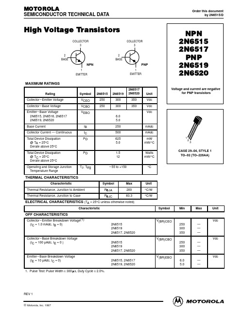
2N6515, 2N6517
2N6519, 2N6520
100 70 50 TJ = 25°C VCE = – 20 V f = 20 MHz
30 20
30 20
10 1.0
2.0
3.0 5.0 7.0 10 20 30 IC, COLLECTOR CURRENT (mA)
50 70
100
10 –1.0
ON CHARACTERISTICS(1)
DC Current Gain (IC = 1.0 mAdc, VCE = 10 Vdc) hFE 2N6515 2N6519 2N6517, 2N6520 2N6515 2N6519 2N6517, 2N6520 2N6515 2N6519 2N6517, 2N6520 2N6515 2N6519 2N6517, 2N6520 2N6515 2N6519 2N6517, 2N6520 VCE(sat) — — — — VBE(sat) — — — VBE(on) — 0.75 0.85 0.90 2.0 Vdc 0.30 0.35 0.50 1.0 Vdc 35 30 20 50 45 30 50 45 30 45 40 20 25 20 15 — — — — — — 300 270 200 220 200 200 — — — Vdc —
2
Motorola Small–Signal Transistors, FETs and Diodes Device Data
பைடு நூலகம்
元器件交易网
NPN 2N6515
200 VCE = 10 V TJ = 125°C hFE, DC CURRENT GAIN
NPN 2N6515 2N6517 PNP 2N6519 2N6520
2N2369中文资料
ft
VCE=10V,IC=10mA, f=100MHz
Output Capacitance
Cobo
VCB=5V, IE=0, f=140kHz
2N2369/2369A
2N2369 2N2369A UNIT
-
40-120
-
>30
-
>20
>20
-
>500 <4.0
>500 <4.0
MHZ pF
Turn on Time Turn off Time
40-120 -
>20
UNIT V V V V nA uA nA nA V V V V V V V V V
page : 1
元器件交易网
ELECTRICAL CHARACTERISTICS (Ta=25 deg C Unless Otherwise Specified)
DESCRIPTION
SYMBOL TEST CONDITION
2N2369
Collector -Emitter Voltage
VCEO*(sus)IC=10mA, IB=0
>15
Collector -Emitter Voltage
VCES
IC=10uA, VBE=0
>40
Collector -Base Voltage
Base Emitter Saturation Voltage
VBE(Sat) * IC=10mA,IB=1mA
0.7-0.85
IC=30mA,IB=3mA
-
IC=100mA,IB=10mA
-
IC=10mA,IB=1mA,Ta= +125 deg C -
2N5401中文资料_数据手册_参数

2N5401中⽂资料_数据⼿册_参数DATA SHEETProduct speci?cationSupersedes data of 1997 May 221999Apr 08DISCRETE SEMICONDUCTORS2N5401PNP high-voltage transistorbook, halfpageM3D186PNP high-voltage transistor2N5401FEATURESLow current (max. 300mA)High voltage (max. 150V).APPLICATIONSGeneral purpose switching and amplification Telephony applications.DESCRIPTIONPNP high-voltage transistor in a TO-92; SOT54 plastic package. NPN complement: 2N5551.PINNING PIN DESCRIPTION1collector2base3emitterFig.1Simplified outline (TO-92; SOT54)and symbol.handbook, halfpage132MAM280123LIMITING VALUESIn accordance with the Absolute Maximum Rating System (IEC134).SYMBOL PARAMETER CONDITIONS MIN.MAX.UNIT V CBO collector-base voltage open emitter??160V V CEO collector-emitter voltage open base??150VV EBO emitter-base voltage open collector??5VI C collector current (DC)??300mAI CM peak collector current??600mAI BM peak base current??100mAP tot total power dissipation T amb≤25°C?630mWT stg storage temperature?65+150°CT j junction temperature?150°CT amb operating ambient temperature?65+150°CPNP high-voltage transistor2N5401THERMAL CHARACTERISTICS Note1.Transistor mounted on an FR4 printed-circuit board.CHARACTERISTICST amb =25°C unless otherwise speci?ed.SYMBOL PARAMETERCONDITIONS VALUE UNIT R th j-a thermal resistance from junction to ambientnote 1200K/WSYMBOL PARAMETERCONDITIONSMIN.MAX.UNIT I CBO collector cut-off current I E =0; V CB =?120V50nA I E =0; V CB =?120V; T amb =100°C 50µA I EBO emitter cut-off current I C =0; V EB =?4V50nAh FEDC current gainI C =?1mA; V CE =?5V; see Fig.250?I C =?10mA; V CE =?5V; see Fig.260240I C =?50mA; V CE =?5V; see Fig.250?V CEsat collector-emitter saturation voltage I C =?10mA; I B =?1mA200mV I C =?50mA; I B =?5mA500mV C c collector capacitance I E =i e =0; V CB =?10V; f =1MHz ?6pF f T transition frequency I C =?10mA; V CE =? 10V; f =100MHz 100300MHz Fnoise ?gureI C =?200µA; V CE =?5V; R S =2k ?;f =10Hz to 15.7kHz8pFPNP high-voltage transistor 2N5401Fig.2 DC current gain; typical values.handbook, full pagewidth015020050100MGD813101110102103h FEI C mAV CE = ?5 VPNP high-voltage transistor2N5401PACKAGE OUTLINEUNIT A REFERENCESOUTLINE VERSION EUROPEAN PROJECTIONISSUE DATE IECJEDEC EIAJ mm5.25.0b 0.480.40c 0.450.40D 4.84.4d 1.71.4E 4.23.6L 14.512.7e 2.54e 11.27L 1(1)2.5b 10.660.56DIMENSIONS (mm are the original dimensions)Note1. Terminal dimensions within this zone are uncontrolled to allow for flow of plastic and terminal irregularities. SOT54SC-4397-02-28AL0 2.5 5 mmscalebcDb 1L 1dE Plastic single-ended leaded (through hole) package; 3 leadsSOT54e 1e123PNP high-voltage transistor2N5401DEFINITIONSData sheet statusObjective speci?cation This data sheet contains target or goal speci?cations for product development. Preliminary speci? cation This data sheet contains preliminary data; supplementary data may be published later. Product speci?cation This data sheet contains ?nal product speci?cations.Limiting valuesLimiting values given are in accordance with the Absolute Maximum Rating System (IEC 134). Stress above one or more of the limiting values may cause permanent damage to the device. These are stress ratings only and operation of the device at these or at any other conditions above those given in the Characteristics sections of the speci?cation is not implied. Exposure to limiting values for extended periods may affect device reliability.Application informationWhere application information is given, it is advisory and does not form part of the speci?cation.LIFE SUPPORT APPLICATIONSThese products are not designed for use in life support appliances, devices, or systems where malfunction of these products can reasonably be expected to result in personal injury. Philips customers using or selling these products for use in such applications do so at their own risk and agree to fully indemnify Philips for any damages resulting from such improper use or sale.PNP high-voltage transistor2N5401Internet: /doc/eacdd8a926d3240c844769eae009581b6ad9bdd4.htmlPhilips Semiconductors – a worldwide companyPhilips Electronics N.V. 1999SCA63All rights are reserved. Reproduction in whole or in part is prohibited without the prior written consent of the copyright owner.The information presented in this document does not form part of any quotation or contract, is believed to be accurate and reliable and may be changed without notice. No liability will be accepted by the publisher for any consequence of its use. Publication thereof does not convey nor imply any license under patent- or other industrial or intellectual property rights.Netherlands: Postbus 90050, 5600PB EINDHOVEN, Bldg.VB,Tel.+31402782785,Fax.+31402788399New Zealand: 2Wagener Place, C.P.O.Box 1041, AUCKLAND,Tel.+6498494160,Fax.+6498497811Norway: Box 1, Manglerud 0612, OSLO,Tel.+4722748000,Fax.+4722748341Pakistan: see SingaporePhilippines: Philips Semiconductors Philippines Inc.,106Valero St.Salcedo Village, P.O.Box 2108MCC,MAKATI,Metro MANILA, Tel.+6328166380,Fax.+6328173474Poland: Ul.Lukiska 10, PL 04-123WARSZAWA,Tel.+48226122831,Fax.+48226122327Portugal: see Spain Romania: see Italy Russia: Philips Russia, /doc/eacdd8a926d3240c844769eae009581b6ad9bdd4.html atcheva 35A, 119048MOSCOW,Tel.+70957556918,Fax.+70957556919Singapore: Lorong 1, Toa Payoh, SINGAPORE 319762,Tel.+653502538,Fax.+652516500Slovakia: see Austria Slovenia: see ItalySouth Africa: S.A. PHILIPS Pty Ltd., 195-215Main Road Martindale,2092JOHANNESBURG, P.O.Box 7430 Johannesburg 2000,Tel.+27114705911,Fax.+27114705494South America: Al.Vicente Pinzon,173, 6th floor,04547-130S?O PAULO,SP, Brazil,Tel.+55118212333,Fax.+55118212382Spain: Balmes 22, 08007BARCELONA,Tel.+34933016312,Fax.+34933014107Sweden: Kottbygatan 7, Akalla, S-16485STOCKHOLM,Tel.+46859852000,Fax.+46859852745Switzerland: Allmendstrasse 140, CH-8027ZüRICH,Tel.+4114882741Fax.+4114883263Taiwan: Philips Semiconductors, 6F, No.96, Chien Kuo N.Rd.,Sec.1,TAIPEI, TaiwanTel.+886221342886,Fax.+886221342874Thailand: PHILIPS ELECTRONICS (THAILAND) Ltd.,209/2Sanpavuth-Bangna Road Prakanong, BANGKOK 10260,Tel.+6627454090,Fax.+6623980793Turkey: Talatpasa Cad. No.5, 80640GüLTEPE/ISTANBUL,Tel.+902122792770,Fax.+902122826707Ukraine : PHILIPS UKRAINE, 4Patrice Lumumba str., Building B, Floor 7,252042KIEV, Tel.+380442642776, Fax.+380442680461United Kingdom: Philips Semiconductors Ltd., 276Bath Road, Hayes,MIDDLESEX UB35BX,Tel.+441817305000,Fax.+441817548421United States: 811East Arques Avenue, SUNNYVALE, CA 94088-3409,Tel.+18002347381, Fax.+18009430087Uruguay: see South AmericaVietnam: see SingaporeYugoslavia: PHILIPS, Trg N. Pasica 5/v, 11000BEOGRAD,Tel.+38111625344,Fax.+38111635777For all other countries apply to: Philips Semiconductors,International Marketing &Sales Communications,Building BE-p, P.O.Box 218,5600MD EINDHOVEN, The Netherlands,Fax.+31402724825Argentina: see South AmericaAustralia: 34 Waterloo Road, NORTH RYDE, NSW 2113,Tel.+61298054455,Fax.+61298054466Austria:Computerstr. 6, A-1101 WIEN, P.O. Box 213,Tel.+431601011248, Fax.+431601011210Belarus: Hotel Minsk Business Center, Bld.3, r.1211, Volodarski Str.6,220050MINSK,Tel.+375172200733,Fax.+375172200773Belgium: see The Netherlands Brazil:see South AmericaBulgaria:Philips Bulgaria Ltd., Energoproject, 15th floor,51James Bourchier Blvd.,1407SOFIA,Tel.+3592689211,Fax.+3592689102Canada: PHILIPS SEMICONDUCTORS/COMPONENTS,Tel.+18002347381, Fax.+18009430087China/Hong Kong: 501Hong Kong Industrial Technology Centre,72Tat Chee Avenue, Kowloon Tong, HONGKONG,Tel.+852********,Fax.+852********Colombia: see South America Czech Republic: see AustriaDenmark: Sydhavnsgade 23, 1780COPENHAGEN V,Tel.+4533293333,Fax.+4533293905Finland: Sinikalliontie 3, FIN-02630ESPOO,Tel.+3589615800,Fax.+358961580920France: 51Rue Carnot, BP317, 92156SURESNES Cedex,Tel.+33140996161,Fax.+33140996427Germany: Hammerbrookstra?e 69, D-20097HAMBURG,Tel.+4940235360,Fax.+494023536300Hungary:see AustriaIndia: Philips INDIA Ltd, Band Box Building, 2nd floor,254-D,Dr.Annie Besant Road, Worli, MUMBAI400025,Tel.+91224938541,Fax.+91224930966Indonesia: PT Philips Development Corporation, Semiconductors Division,Gedung Philips, Jl. Buncit Raya Kav.99-100, JAKARTA 12510,Tel.+62217940040ext.2501, Fax.+62217940080Ireland: Newstead, Clonskeagh, DUBLIN14,Tel.+35317640000,Fax.+35317640200Israel: RAPAC Electronics, 7Kehilat Saloniki St, PO Box 18053,TEL AVIV 61180,Tel.+97236450444,Fax.+97236491007Italy: PHILIPS SEMICONDUCTORS, Piazza IV Novembre 3,20124MILANO,Tel.+39267522531,Fax.+39267522557Japan: Philips Bldg 13-37, Kohnan 2-chome, Minato-ku,TOKYO 108-8507, Tel.+81337405130,Fax.+81337405077Korea: Philips House, 260-199Itaewon-dong, Yongsan-ku, SEOUL,Tel.+8227091412,Fax.+8227091415Malaysia: No.76Jalan Universiti, 46200PETALING JAYA, SELANGOR,Tel.+60 37505214,Fax.+6037574880Mexico: 5900Gateway East, Suite 200, EL PASO, TEXAS 79905,Tel.+9-58002347381, Fax +9-58009430087Middle East: see ItalyPrinted in The Netherlands115002/00/03/pp8 Date of release: 1999Apr 08Document order number: 939775005406万联芯城专注电⼦元器件配单服务,只售原装现货库存,万联芯城在业内有三⼗年电⼦元器件配单经验,客户遍布全国,物料供应链完善,元器件价格优势明显,原装质量有保障,电⼦元器件⼀站式采购可为客户省去逐个查找环节,只需提供BOM 表,即可为您报价,整单采购可节省成本,万联芯城完善的产品供应链体系可以应对多种不同物料需求的报价,点击进⼊万联芯城。
2SK3419-E中文资料

2SK3419Silicon N Channel MOS FETHigh Speed Power SwitchingREJ03G1099-0200(Previous: ADE-208-942)Rev.2.00Sep 07, 2005 Features• Low on-resistanceR DS (on) = 4.3 mΩ typ.• 4 V gate drive device• High speed switchingOutlineAbsolute Maximum Ratings(Ta = 25°C)Item Symbol Value UnitDrain to source voltage V DSS 60 V Gate to source voltage V GSS ±20 V Drain current I D 90 A Drain peak current I D (pulse) Note 1 360 A Body-drain diode reverse drain current I DR 90 A Avalanche current I AP Note 3 65 A Avalanche energy E AR Note 3 362 mJ Channel dissipation Pch Note 2 150 W Channel temperature Tch 150 °C Storage temperature Tstg –55 to +150 °C Notes: 1. PW ≤ 10 µs, duty cycle ≤ 1% 2. Value at Tc = 25°C 3. Value at Tch = 25°C, Rg ≥ 50 ΩElectrical Characteristics(Ta = 25°C)Item Symbol Min Typ Max Unit Test ConditionsDrain to source breakdown voltage V (BR) DSS 60 — — V I D = 10 mA, V GS = 0 Zero gate voltage drain current I DSS — — 10 µA V DS = 60 V, V GS = 0 Gate to source leak current I GSS — — ±0.1 µA V GS = ±20 V, V DS = 0 Gate to source cutoff voltage V GS (off) 1.0 — 2.5 V V DS = 10 V, I D = 1 mA Note 4 Forward transfer admittance |y fs | 55 90 — S I D = 45 A, V DS = 10 V Note 4 R DS (on) — 4.3 5.5 m Ω I D = 45 A, V GS = 10 V Note 4Static drain to source on state resistance R DS (on) — 6.0 9.0 m Ω I D = 45 A, V GS = 4 V Note 4Input capacitance Ciss — 9770 — pF Output capacitance Coss — 1340 — pFReverse transfer capacitance Crss — 470 — pFV DS = 10 VV GS = 0 f = 1 MHz Total gate charge Qg — 180 — nC Gate to source charge Qgs — 32 — nCGate to drain charge Qgd — 36 — nC V DD = 50 VV GS = 10 V I D = 90 A Turn-on delay timet d (on) — 53 — ns Rise timet r — 320 — nsTurn-off delay time t d (off) — 700 — nsFall timet f — 380 — nsV GS = 10 VI D = 45 A R L = 0.67 Ω Body-drain diode forward voltageV DF — 1.0 — V I F = 90 A, V GS = 0 Body-drain diode reverse recovery time t rr — 75 — ns I F = 90 A, V GS = 0di F /dt = 50 A/µsNote: 4. Pulse testMain CharacteristicsPackage DimensionsOrdering InformationPart Name Quantity Shipping Container2SK3419-E 30 pcs Plastic magazineNote: For some grades, production may be terminated. Please contact the Renesas sales office to check the state of production before ordering the product. RENESAS SALES OFFICESRefer to "/en/network" for the latest and detailed information.Renesas Technology America, Inc.450 Holger Way, San Jose, CA 95134-1368, U.S.ATel: <1> (408) 382-7500, Fax: <1> (408) 382-7501Renesas Technology Europe LimitedDukes Meadow, Millboard Road, Bourne End, Buckinghamshire, SL8 5FH, U.K.Tel: <44> (1628) 585-100, Fax: <44> (1628) 585-900Renesas Technology Hong Kong Ltd.7th Floor, North Tower, World Finance Centre, Harbour City, 1 Canton Road, Tsimshatsui, Kowloon, Hong KongTel: <852> 2265-6688, Fax: <852> 2730-6071Renesas Technology Taiwan Co., Ltd.10th Floor, No.99, Fushing North Road, Taipei, TaiwanTel: <886> (2) 2715-2888, Fax: <886> (2) 2713-2999Renesas Technology (Shanghai) Co., Ltd.Unit2607 Ruijing Building, No.205 Maoming Road (S), Shanghai 200020, ChinaTel: <86> (21) 6472-1001, Fax: <86> (21) 6415-2952Renesas Technology Singapore Pte. Ltd.1 Harbour Front Avenue, #06-10, Keppel Bay Tower, Singapore 098632Tel: <65> 6213-0200, Fax: <65> 6278-8001Renesas Technology Korea Co., Ltd.Kukje Center Bldg. 18th Fl., 191, 2-ka, Hangang-ro, Yongsan-ku, Seoul 140-702, KoreaTel: <82> 2-796-3115, Fax: <82> 2-796-2145Renesas Technology Malaysia Sdn. Bhd.Unit 906, Block B, Menara Amcorp, Amcorp Trade Centre, No.18, Jalan Persiaran Barat, 46050 Petaling Jaya, Selangor Darul Ehsan, MalaysiaTel: <603> 7955-9390, Fax: <603> 7955-9510。
2N3810DCSM中文资料

DUAL HIGH GAIN PNP TRANSISTORS IN A HERMETICALL Y SEALEDCERAMIC SURFACE MOUNT PACKAGE FOR HIGH RELIABILITY APPLICATIONSFEATURES• HERMETIC CERAMIC SURFACE MOUNT PACKAGE• CECC SCREENING OPTIONS• SPACE QUALITY LEVELS OPTIONSAPPLICATIONS:Suitable for use in high gain, low noise differential amplifier applications.V CBO Collector – Base Voltage V CEO Collector – Emitter Voltage 1V EBO Emitter – Base Voltage I C Collector CurrentP D Total Device Dissipation Derate above 25°CT STGStorage Temperature Range–60V –60V –5V –50mA 500mW 600mW 2.9mW / °C 3.4mW / °C–65 to 200°CMECHANICAL DATADimensions in mm (inches)LCC2 PACKAGEUnderside ViewABSOLUTE MAXIMUM RATINGS(T amb = 25°C unless otherwise stated)PAD 1 – Collector 1PAD 2 – Base 1PAD 3 – Base 2PAD 4 – Collector 2PAD 5 – Emitter 2PAD 6 – Emitter 1NOTES1. Base – Emitter Diode Open Circuited.EACH SIDE TOT AL DEVICELABParameterTest Conditions 1Min.Typ.Max.UnitVnA µA nA—V V k Ω—µmho—pF–60–60–5–10–10–2010015045075150450150450125–0.7–0.7–0.8–0.2–0.2533015060025 x 10-456011548V (BR)CBO Collector – Base Breakdown Voltage V (BR)CEO*Collector – Emitter Breakdown Voltage V (BR)EBO Emitter – Base Breakdown Voltage I CBO Collector Cut-off Current I EBOEmitter Cut-off Currenth FEDC Current GainV BEBase – Emitter VoltageV CE(sat)Collector – Emitter Saturation Voltage h ie Small Signal Common – Emitter Input Impedanceh fe Small Signal Common – Emitter Current Gainh re Small Signal Common – Emitter Reverse Voltage Gainh oeSmall Signal Common – Emitter Output Admittance|h fe |Small Signal Common – Emitter Current GainC obo Common – Base Open Circuit Output CapacitanceC ibo Common – Base Open Circuit Input CapacitanceI C = –10µA I E = 0I C = –10mA I B = 0I E = –10µA I C = 0V CB = –50VI E = 0T A = 150°CV EB = –4V I C = 0I C = –10µA V CE = –5V I C = –100µAV CE = –5V T A = –55°C I C = –500µA V CE = –5V I C = –1mA V CE = –5V I C = –10mA V CE = –5V *I C = –100µAV CE = –5V I B = –10µA I C = –100µA I B = –100µAI C = –1mA I B = –10µA I C = –100µA I B = –100µAI C = –1mAV CE = –10VI C = –1mA f = 1kHzV CE = –5VI C = –500µAf = 30MHz V CE = –5V I C = –1mA f = 100MHz V CB = –5V I E = 0f = 100kHz V EB = –0.5V I C = 0f = 100kHzELECTRICAL CHARACTERISTICS (T amb = 25°C unless otherwise stated)NOTES* Pulse Test: t p = 300µs, δ≤2%.1) Terminals not under test are open circuited under all test conditions.INDIVIDUAL TRANSISTOR CHARACTERISTICSLABELECTRICAL CHARACTERISTICS (T amb = 25°C unless otherwise stated)NOTES1) Terminals not under test are open circuited under all test conditions.2) The lower of the two readings is taken as h FE1.3) Average noise figure is measured in an amplifier with response down 3dB at 10Hz and 10 kHz and a high frequency rolloff of 6dB / octave.ParameterTest ConditionsMin.Typ.Max.Unit—mVmV 0.91530.81h FE1Static Forward Current Gain h FE2Balance Ratio|V BE1– V BE2|Base – Emitter Voltage Differential|∆(V BE1– V BE2)∆T A |Base – Emitter Voltage DifferentialV CE = –5V I C = –100µASee Note 2.V CE = –5VI C = –10µA to –10mA V CE = –5V I C = –100µA V CE = –5V I C = –100µA T A1= 25°C T A2= –55°C V CE = –5V I C = –100µA T A1= 25°CT A2= 125°CTRANSISTOR MATCHING CHARACTERISTICS OPERATING CHARACTERISTICS (T amb = 25°C unless otherwise stated)ParameterTest Conditions 1Min.Typ.Max.UnitdBdB732.53.5FSpot Noise Figure_FAverage Noise FigureV CE = –10VI C = –100µA R G = 3k Ω f = 100Hz Noise Bandwidth = 20HzV CE = –10VI C = –100µA R G = 3k Ω f = 1kHz Noise Bandwidth = 200HzV CE = –10V I C = –100µA R G = 3k Ω f = 10kHz Noise Bandwidth = 2kHzV CE = –10VI C = –100µAR G = 3k ΩNoise Bandwidth = 15.7kHz See Note 3.INDIVIDUAL TRANSISTOR CHARACTERISTICSLABTHERMAL INFORMATION2550751001251501752000.00.10.20.30.40.50.60.70.8T Free Air Temperature (˚C)AP M a x i m u m C o n t i n u o u s D i s s i p a t i o n (W )T TOTAL DEVICEEACHTRANSISTOR。
2SK3497中文资料
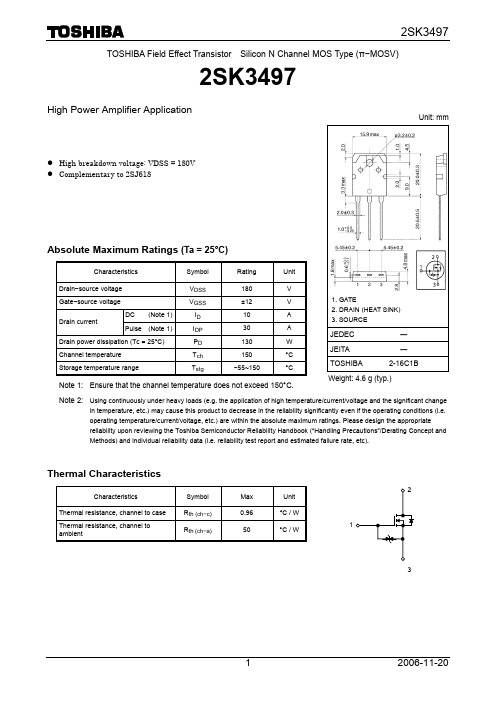
TOSHIBA Field Effect Transistor Silicon N Channel MOS Type (π−MOSV)2SK3497High Power Amplifier Applicationz High breakdown voltage: VDSS = 180V z Complementary to 2SJ618Absolute Maximum Ratings (Ta = 25°C)Characteristics Symbol Rating UnitDrain −source voltage V DSS 180 VGate −source voltage V GSS ±12 V DC (Note1) I D 10 ADrain currentPulse (Note 1) I DP 30A Drain power dissipation (Tc = 25°C) P D 130 W Channel temperature T ch 150 °C Storage temperature rangeT stg−55~150 °CNote 1: Ensure that the channel temperature does not exceed 150°C.Note 2: Using continuously under heavy loads (e.g. the application of high temperature/current/voltage and the significant changein temperature, etc.) may cause this product to decrease in the reliability significantly even if the operating conditions (i.e. operating temperature/current/voltage, etc.) are within the absolute maximum ratings. Please design the appropriate reliability upon reviewing the Toshiba Semiconductor Reliability Handbook (“Handling Precautions”/Derating Concept and Methods) and individual reliability data (i.e. reliability test report and estimated failure rate, etc).Thermal CharacteristicsCharacteristics Symbol Max UnitThermal resistance, channel to case R th (ch −c) 0.96 °C / W Thermal resistance, channel toambientR th (ch −a)50°C / WUnit: mm1.GATE 2. DRAIN (HEAT SINK)3. SOURCEJEDEC ― JEITA―TOSHIBA 2-16C1B Weight: 4.6 g (typ.)3Electrical Characteristics (Ta = 25°C)Characteristics SymbolTest ConditionMin Typ. Max Unit Gate leakage current I GSS V GS = ±12 V, V DS = 0 V — —10 μA Drain cut −off currentI DSS V DS = 180V, V GS = 0 V — — 100μA Drain −source breakdown voltage V (BR) DSS I D = 10 mA, V GS = 0 V 180 — — V Gate threshold voltage V th V DS = 10 V, I D = 1 mA 1.1 — 2.1 V Drain −source saturation voltage V DS (ON)V GS = 7 V, I D = 5 A— — 0.75V Forward transfer admittance |Y fs | V DS = 10 V, I D = 5 A6.012.0—SInput capacitanceC iss — 2400 —Reverse transfer capacitance C rss — 220 — Output capacitanceC ossV DS = 30 V, V GS = 0 V, f = 1 MHz — 30 —pF This transistor is an electrostatic-sensitive device. Please handle with caution.Markinglead (Pb)-free package or lead (Pb)-free finish.RESTRICTIONS ON PRODUCT USE20070701-EN •The information contained herein is subject to change without notice.•TOSHIBA is continually working to improve the quality and reliability of its products. Nevertheless, semiconductor devices in general can malfunction or fail due to their inherent electrical sensitivity and vulnerability to physical stress. It is the responsibility of the buyer, when utilizing TOSHIBA products, to comply with the standards of safety in making a safe design for the entire system, and to avoid situations in which a malfunction or failure of such TOSHIBA products could cause loss of human life, bodily injury or damage to property.In developing your designs, please ensure that TOSHIBA products are used within specified operating ranges as set forth in the most recent TOSHIBA products specifications. Also, please keep in mind the precautions and conditions set forth in the “Handling Guide for Semiconductor Devices,” or “TOSHIBA Semiconductor Reliability Handbook” etc.• The TOSHIBA products listed in this document are intended for usage in general electronics applications (computer, personal equipment, office equipment, measuring equipment, industrial robotics, domestic appliances, etc.).These TOSHIBA products are neither intended nor warranted for usage in equipment that requires extraordinarily high quality and/or reliability or a malfunction or failure of which may cause loss of human life or bodily injury (“Unintended Usage”). Unintended Usage include atomic energy control instruments, airplane or spaceship instruments, transportation instruments, traffic signal instruments, combustion control instruments, medical instruments, all types of safety devices, etc.. Unintended Usage of TOSHIBA products listed in his document shall be made at the customer’s own risk.•The products described in this document shall not be used or embedded to any downstream products of which manufacture, use and/or sale are prohibited under any applicable laws and regulations.• The information contained herein is presented only as a guide for the applications of our products. No responsibility is assumed by TOSHIBA for any infringements of patents or other rights of the third parties which may result from its use. No license is granted by implication or otherwise under any patents or other rights of TOSHIBA or the third parties.• Please contact your sales representative for product-by-product details in this document regarding RoHS compatibility. Please use these products in this document in compliance with all applicable laws and regulations that regulate the inclusion or use of controlled substances. Toshiba assumes no liability for damage or losses occurring as a result of noncompliance with applicable laws and regulations.。
2N4117A中文资料(Calogic)中文数据手册「EasyDatasheet - 矽搜」

Part
Hale Waihona Puke 包裹2N4117-19 / A密封TO-72 PN4117-19 / A塑料TO-92 SST4117-19塑料SOT-23 X2N4117-19 / A排序芯片载体
温度范围
-55oC至175 oC -55oC至+135 oC -55oC至+135 oC -55oC至175 oC
电气特性
(TA = 25 oC除非另有说明)
(TA = 25oC除非另有说明)
门源或门极 - 漏极电压. . . . . . . . . . . . . . . . -40V
栅电流. . . . . . . . . . . . . . . . . . . . . . . . . . . . . . . . . 50毫安
存储温度范围. . . . . . . . . . . . . -65
芯片中文手册,看全文,戳
N沟道JFET
通用放大器
LLC
引脚配置
5007
2N4117 – 2N4119 / 2N4117A – 2N4119A PN4117 – PN4119 / PN4117A – PN4119A / SST4117 – SST4119
特征
低 电 容漏 出
Low
绝对最大额定值
最小值最大值最小值最大值最小值最大值
测试条件
-40
-40
-40
V IG = -1µA, V DS = 0
-10
-10
-10
pA
-1
-1
-1
VGS = -20V, V DS = 0
-25
-25
-25
nA
-2.5
-2.5
2N4392中文资料

Min.
40
Typ.
Max. Unit
V 0.1 0.2 nA
IG = 1.0mA VGS = 20V VGS = 20V VDS = 20V IG = 1.0mA VGS = 7V VGS = 7V
VDS = 0 VDS = 0 VDS = 0 TA = 150°C ID = 1.0nA VDS = 0 VDS = 20V VDS = 20V TA = 150°C
VDS VDG VGS IGF PD TJ TSTG Drain–Source Voltage Drain–Gate Voltage Gate–Source Voltage Forward Gate Current Total Device Dissipation @ TC = 25°C Derate above 25°C Operating Junction Temperature Range Storage Temperature Range 40V 40V 40V 50mA 1.8W 10mW/ °C –65 to +175°C –65 to +175°C
2N4392
ELECTRICAL CHARACTERISTICS (TA = 25°C unless otherwise stated) Parameter Test Conditions
OFF CHARACTERISTICS
V(BR)GSS IGSS VGS VGS(f) ID(off) Gate Source Breakdown Voltage1 Gate Reverse Current Gate Source Voltage Gate Source Forward Voltage
- 1、下载文档前请自行甄别文档内容的完整性,平台不提供额外的编辑、内容补充、找答案等附加服务。
- 2、"仅部分预览"的文档,不可在线预览部分如存在完整性等问题,可反馈申请退款(可完整预览的文档不适用该条件!)。
- 3、如文档侵犯您的权益,请联系客服反馈,我们会尽快为您处理(人工客服工作时间:9:00-18:30)。
MSC0981A.DOC 12-02-98
2N3419
ABSOLUTE MAXIMUM RATINGS:
SYMBOLCHARACTERISTICVALUEUNITS
VCBO*Collector-Base Voltage125Volts
VCEO*Collector-Emitter Voltage80Volts
VEBO*Emitter-Base Voltage8Volts
IC*D.C. Collector Current3Amps
IC*Peak Collector Current5Amps
TSTG*Storage Temperature-65 to 200
°
C
TJ*Operating Junction Temperature-65 to 200
°
C
PT*Power Dissipation
TC = 25°C Ambient
TC = 100°C Case
1.015Watts
Watts
3 Amp, 125V,
NPN Silicon Power
Transistors
JAN, JTX, JTXV, JANS
FEATURES:
•
Meets MIL-S-19500/393
•
Collector-Base Voltage: up to 125V
•
Peak Collector Current: 5A
•
High Power Dissipation in TO-5: 15W @ T
C
= 100°C
•
Fast Switching
TO-5
APPLICATIONS:
•
Power Supply
•
Pulse Amplifier
•
High Frequency Power Switching
7516 Central Industrial Drive
Riviera Beach, Florida
33404
PHONE: (561) 842-0305
FAX: (561) 845-7813
DESCRIPTION:
These power transistors are produced by PPC's DOUBLE
DIFFUSED PLANAR process. This technology produces high
voltage devices with excellent switching speeds, frequency
response, gain linearity, saturation voltages, high current gain,
and safe operating areas. They are intended for use in
Commercial, Industrial, and Military power switching, amplifier,
and regulator applications.
Ultrasonically bonded leads and controlled die mount
techniques are utilized to further increase the SOA capability
and inherent reliability of these devices. The temperature
range to 200°C permits reliable operation in high ambients, and
the hermetically sealed package insures maximum reliability
and long life.
*
Indicates MIL-S-19500/393
元器件交易网www.cecb2b.com
MSC0981A.DOC 12-02-98
2N3419
ELECTRICAL CHARACTERISTICSELECTRICAL CHARACTERISTICS::
(25°Case Temperature Unless Otherwise Noted)
VALUE
SYMBOLCHARACTERISTICTEST CONDITIONSMin.Max.Units
BV
CEO*
Collector-EmitterBreakdown VoltageIC = 50 mAdc, Cond. D (Note 1)80----Vdc
ICEX*Collector-EmitterCutoff CurrentVEB = 0.5 Vdc, Cond. A, VCE = 120 VdcVEB = 0.5 Vdc, Cond. A, TA = 150°C, VCE = 120 Vdc--------0.350µAdc
µ
Adc
I
CEO*
Collector-EmitterCutoff CurrentVCE = 60 Vdc, Cond. D----5.0
µ
Adc
IEBO*
Emitter-BaseCutoff CurrentVEB = 6 Vdc, Cond. DVEB = 8 Vdc, Cond. D--------0.5
10
µ
Adc
µ
Adc
hFE*D.C. Current Gain
(Note 1)
IC = 100 mAdc, VCE = 2 Vdc
IC = 1 Adc, VCE = 2 Vdc
IC = 2 Adc, VCE = 2 Vdc
IC = 5 Adc, VCE = 5 Vdc
IC = 1 Adc, VCE = 2 Vdc, T
A
= - 55°C
2020151010----60----------------
----
----
----
----
VCE(sat)*Collector-EmitterSaturation Voltage(Note 1)IC = 1 Adc, IB = 0.1 Adc
IC = 2 Adc, IB = 0.2 Adc
--------0.250.5Vdc
Vdc
VBE(sat)*Base-Emitter SaturationVoltage (Note 1)IC = 1 Adc, IB = 0.1 Adc
IC = 2 Adc, IB = 0.2 Adc
0.60.71.21.4Vdc
Vdc
I
S/b*
Forward Biased SecondBreakdownVCE = 5 Vdc, TC = 100°CVCE = 37 Vdc, TC = 100°CVCE = 80 Vdc, TC = 100°C3
0.4
120
------------Adc
Adc
mAdc
E
S/b*
Unclamped ReverseBiased SecondBreakdownIC = 3 Adc, L = 10 mH, Base Open45----mj
E
S/b*
clamped Reverse BiasedSecond BreakdownIC = 3 Adc, L = 40 mH, VClamp = 85V125----mj
fT*Gain Bandwidth ProductIC = 0.1 Adc, VCE = 10 Vdc, f = 20 MHz
26160MHz
COb*Output CapacitanceVCB = 10 Vdc, IE = 0, f = 1 MHz----150pf
tonTurn-on TimeIC = 1 Adc, IB1 = - IB2 = 0.1 Adc----0.3µs
toffTurn-off TimeIC = 1 Adc, IB1 = - IB2 = 0.1 Adc
----1.2
µ
s
Note 1:Pulse Test: Pulse width = 300µSec., duty cycle ≤ 2%.
* Indicates MIL-S-19500/393
元器件交易网www.cecb2b.com
MSC0981A.DOC 12-02-98
2N3419
PACKAGE MECHANICAL DATA:
NOTE: DIMENSIONS IN [ ] = MILLIMETERS
Ø.305 [7.75]
Ø.335 [8.51]
1.500 [38.10] MIN
.010 [.25]
.030 [.76]
.240 [6.35]
.260 [6.60]
.100 [2.54]
.100 [2.54]
.200 [5.08]
.029 [.74]
.045 [1.14]
.031 [.79]
45°
Ø.335 [8.51]
Ø.370 [9.40]
Ø.017 [.432]
+.002
-.001
[+.051]
[.025]
元器件交易网www.cecb2b.com